


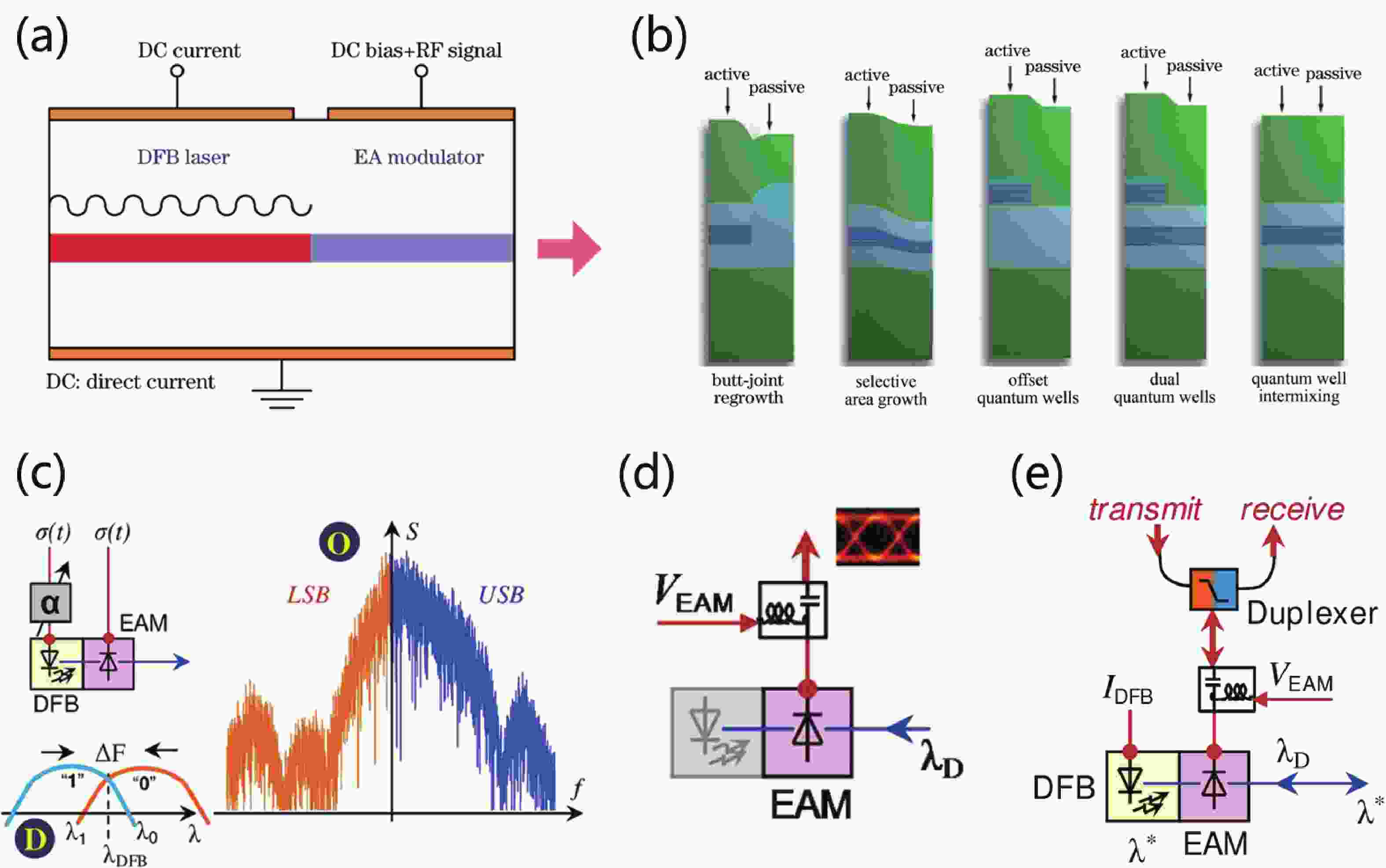
Currently, the global 5G network, cloud computing, and data center industries are experiencing rapid development. The continuous growth of data center traffic has driven the vigorous progress in high-speed optical transceivers for optical interconnection within data centers. The electro-absorption modulated laser (EML), which is widely used in optical fiber communications, data centers, and high-speed data transmission systems, represents a high-performance photoelectric conversion device. Compared to traditional directly modulated lasers (DMLs), EMLs demonstrate lower frequency chirp and higher modulation bandwidth, enabling support for higher data rates and longer transmission distances. This article introduces the composition, working principles, manufacturing processes, and applications of EMLs. It reviews the progress on advanced indium phosphide (InP)-based EML devices from research institutions worldwide, while summarizing and comparing data transmission rates and key technical approaches across various studies.
Silicon photonics is an emerging competitive solution for next-generation scalable data communications in different application areas as high-speed data communication is constrained by electrical interconnects. Optical interconnects based on silicon photonics can be used in intra/inter-chip interconnects, board-to-board interconnects, short-reach communications in datacenters, supercomputers and long-haul optical transmissions. In this paper, we present an overview of recent progress in silicon optoelectronic devices and optoelectronic integrated circuits(OEICs) based on a complementary metal-oxide-semiconductor-compatible process, and focus on our research contributions. The silicon optoelectronic devices and OEICs show good characteristics, which are expected to benefit several application domains, including communication, sensing, computing and nonlinear systems.
We propose a novel all-optical sampling method using nonlinear polarization rotation in a semiconductor optical amplifier.A rate-equation model capable of describing the all-optical sampling mechanism is presented in this paper.Based on this model,we investigate the optimized operating parameters of the proposed system by simulating the output intensity of the probe light as functions of the input polarization angle,the phase induced by the polarization controller,and the orientation of the polarization beam splitter.The simulated results show that we can obtain a good linear slope and a large linear dynamic range,which is suitable for all-optical sampling.The operating power of the pump light can be less than 1mW.The presented all-optical sampling method can potentially operate at a sampling rate up to hundreds GS/s and needs low optical power.
The optical properties of polypyrrole (Ppy) thin films upon 2 MeV electron beam irradiation changes with different doses. The induced changes in the optical properties for Ppy thin films were studied in the visible range 300 to 800 nm at room temperature. The optical band gap of the pristine Ppy was found to be 2.19 eV and it decreases up to 1.97 eV for a 50 kGy dose of 2 MeV electron beam. The refractive index dispersion of the samples obeys the single oscillator model. The obtained results suggest that electron beam irradiation changes the optical parameters of Ppy thin films.
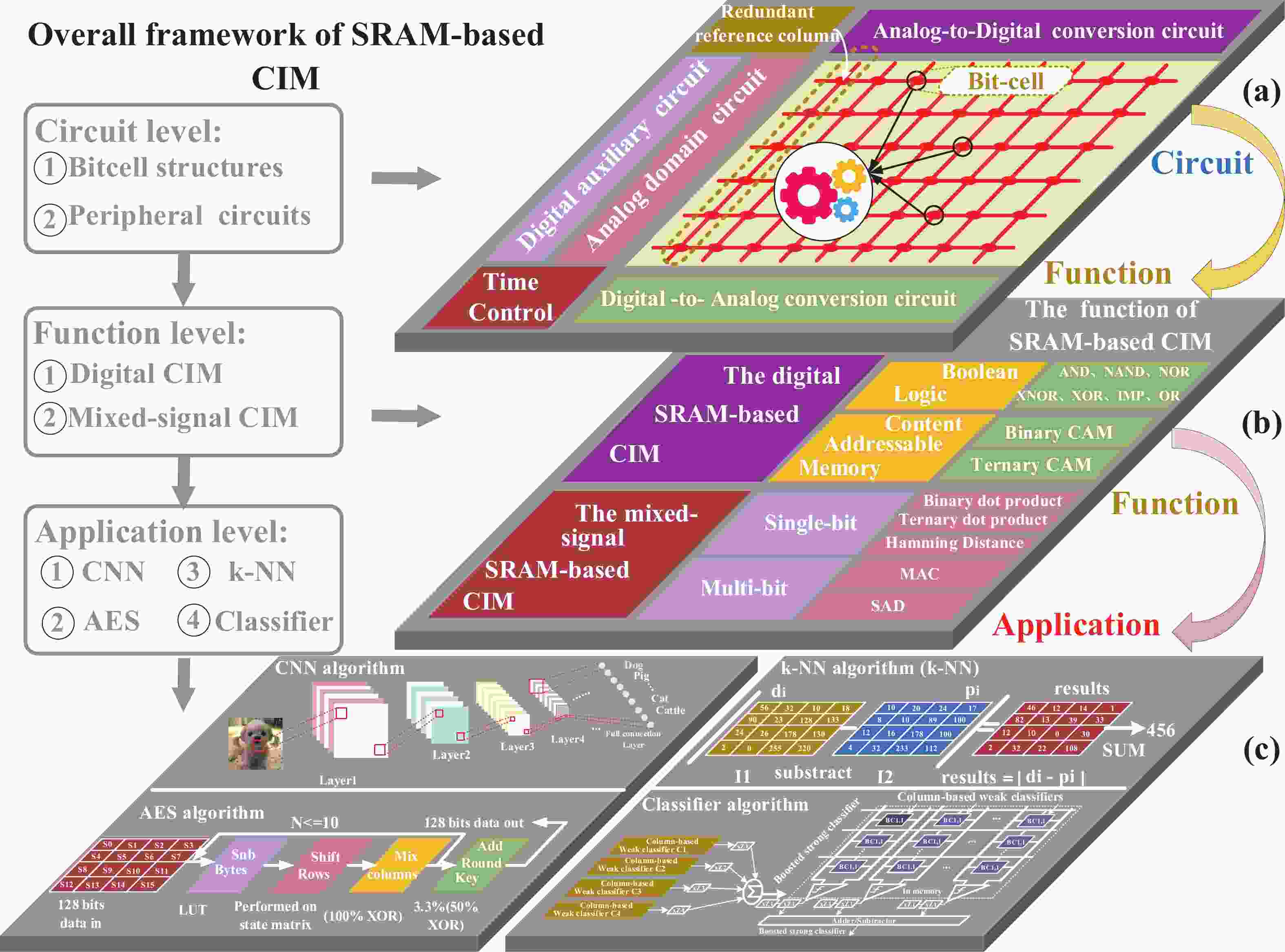
Artificial intelligence (AI) processes data-centric applications with minimal effort. However, it poses new challenges to system design in terms of computational speed and energy efficiency. The traditional von Neumann architecture cannot meet the requirements of heavily data-centric applications due to the separation of computation and storage. The emergence of computing in-memory (CIM) is significant in circumventing the von Neumann bottleneck. A commercialized memory architecture, static random-access memory (SRAM), is fast and robust, consumes less power, and is compatible with state-of-the-art technology. This study investigates the research progress of SRAM-based CIM technology in three levels: circuit, function, and application. It also outlines the problems, challenges, and prospects of SRAM-based CIM macros.
A brief introduction of semiconductor self-assembled quantum dots (QDs) applied in single-photon sources is given. Single QDs in confined quantum optical microcavity systems are reviewed along with their optical properties and coupling characteristics. Subsequently, the recent progresses in In(Ga)As QDs systems are summarized including the preparation of quantum light sources, multiple methods for embedding single QDs into different microcavities and the scalability of single-photon emitting wavelength. Particularly, several In(Ga)As QD single-photon devices are surveyed including In(Ga)As QDs coupling with nanowires, InAs QDs coupling with distributed Bragg reflection microcavity and the In(Ga)As QDs coupling with micropillar microcavities. Furthermore, applications in the field of single QDs technology are illustrated, such as the entangled photon emission by spontaneous parametric down conversion, the single-photon quantum storage, the chip preparation of single-photon sources as well as the single-photon resonance-fluorescence measurements.
Although perovskite solar cells containing methylamine cation can show high power conversion efficiency, stability is a concern. Here, methylamine-free perovskite material CsxFA1–xPbI3 was synthesized by a one-step method. In addition, we incorporated smaller cadmium ions into mixed perovskite lattice to partially replace Pb ions to address the excessive internal strain in perovskite structure. We have found that the introduction of Cd can improve the crystallinity and the charge carrier lifetime of perovskite films. Consequently, a power conversion efficiency as high as 20.59% was achieved. More importantly, the devices retained 94% of their initial efficiency under 1200 h of continuous illumination.

In a recent article, Chen et al. [Electrochimica Acta, 2014, 130: 279] presented their fabrication and characterization results on a graphene/n-Si solar cell where the Au nanoparticles were inserted in graphene to increase its optical and electrical properties. The higher efficiency of the device was attributed to increased conductivity of graphene after doping with Au nanoparticles. However, the knowledge in the field of Schottky diode solar cells relates this to increased band bending at the junction. Also, to explain the instability behaviour, they concluded that the growth of silicon oxide on the Si surface or oxygen adsorption on the window layer resulted in the device performance increasing initially and decreasing in the end. However, this instability seems to be due to variation in series resistance reduced at the beginning because of slightly lowered Fermi level and increased at the end by the self-compensation by deep in-diffusion of Au nanoparticles into n-Si layer. We also propose that inserting a very thin p-type layer at the junction will enhance the carrier collection and performance of this device.


