SEMICONDUCTOR DEVICES
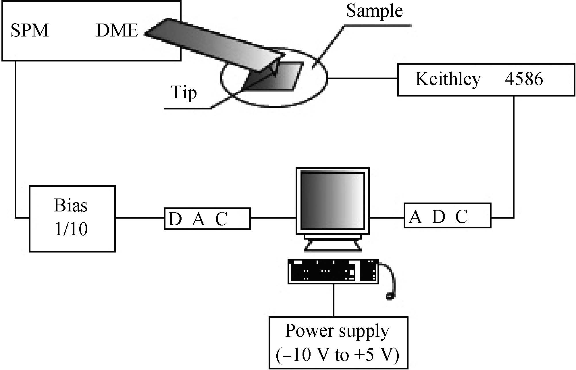
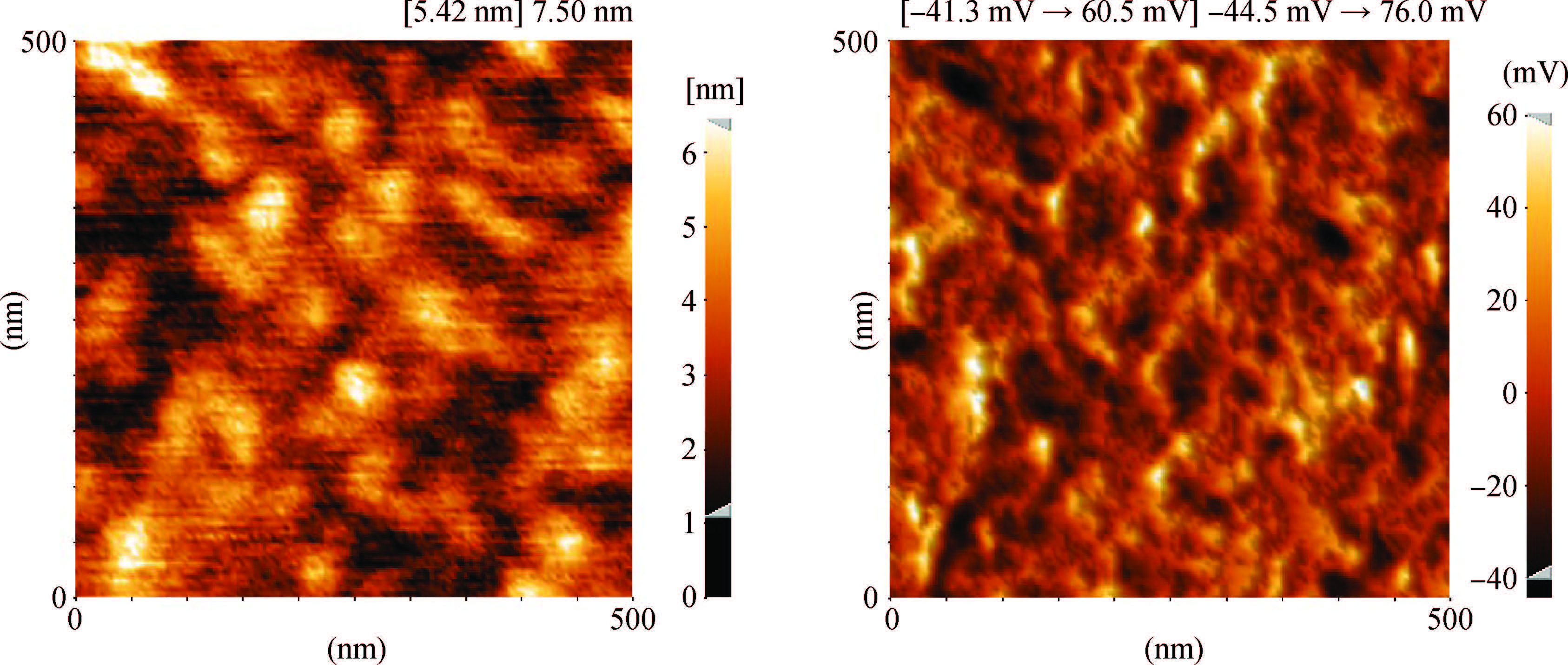
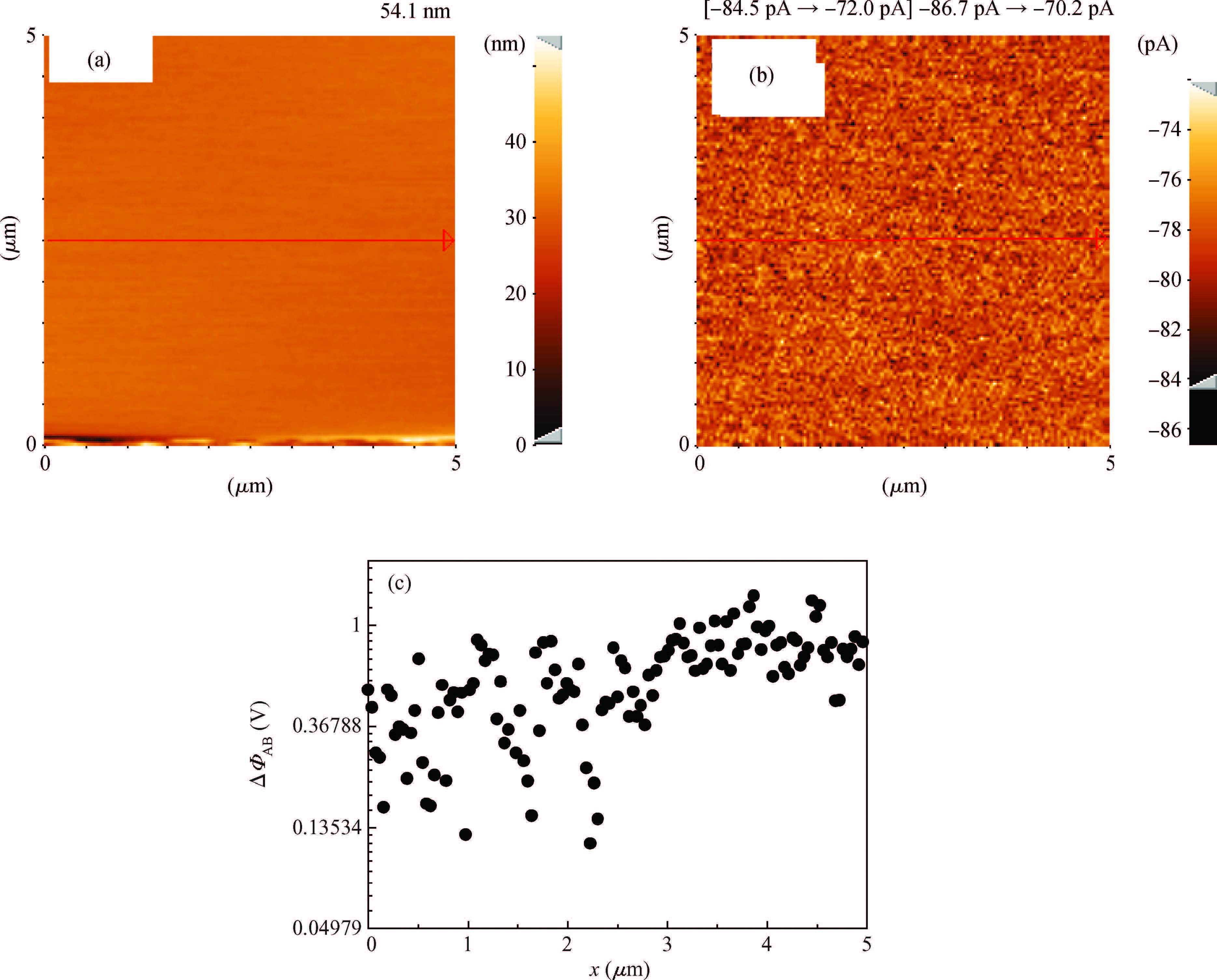
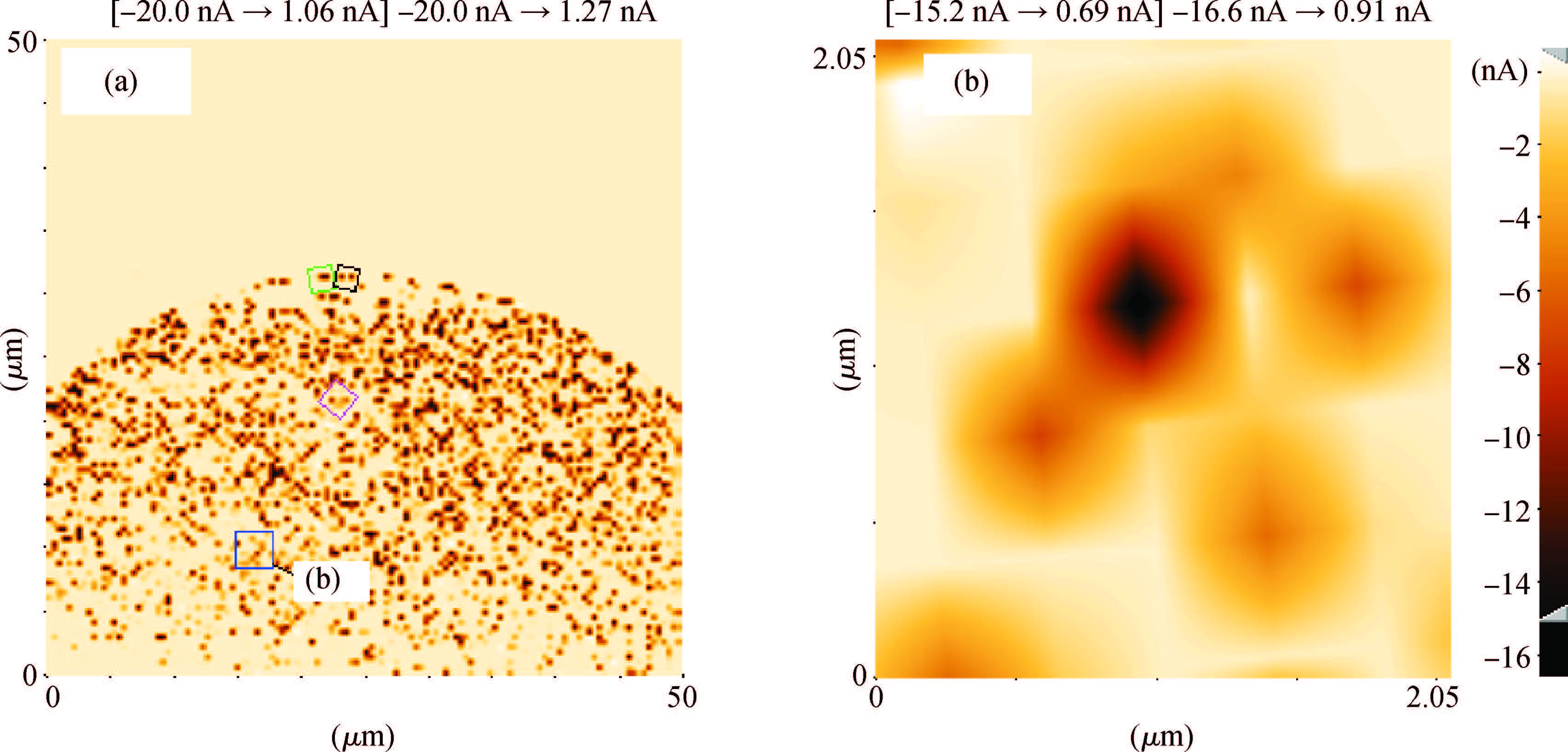
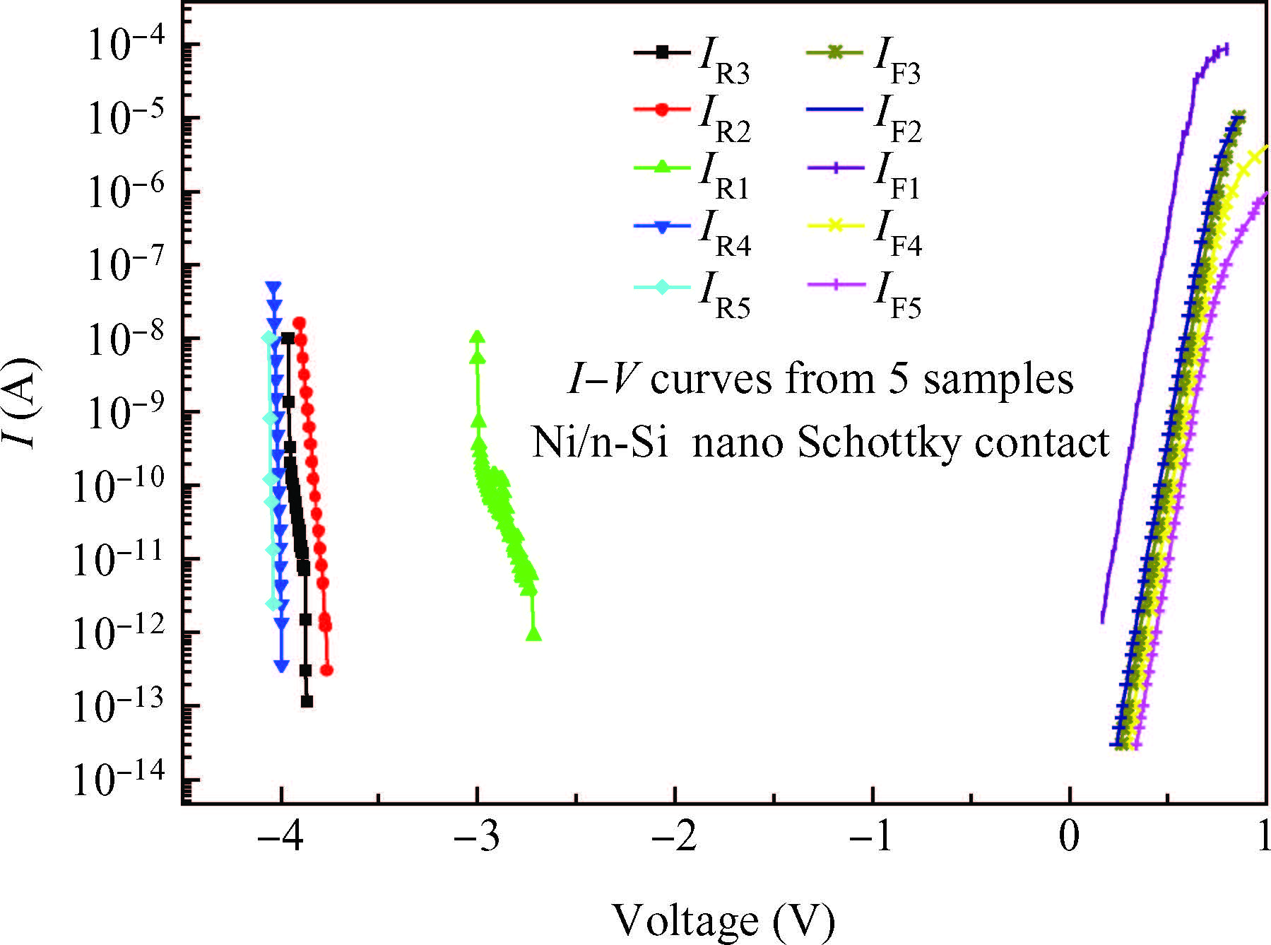
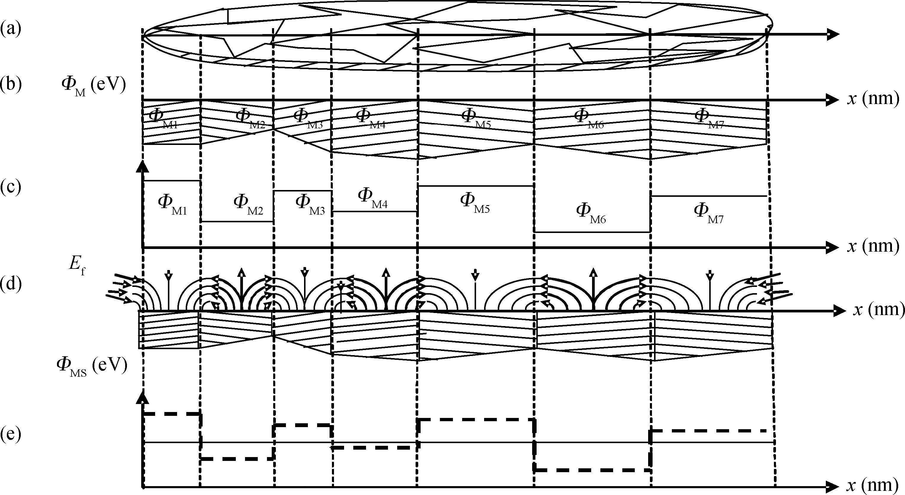
Abstract: We have experimentally studied the Ni/n-Si nano Schottky barrier height(SBH) and potential difference between patches in the nano Schottky diodes(SD) using contact atomic force microscopy(C-AFM) in tapping mode and scanning tunneling microscopy(STM). Topology measurement of the surface with C-AFM showed that, a single Ni/n-Si SD consists of many patches with different sizes. These patches are sets of parallel diodes and electrically interacting contacts of 5 to 50 nm sizes and between these individual diodes, there exists an additional electric field. In real metal semiconductor contacts(MSC), patches with quite different configurations, various geometrical sizes and local work functions were randomly distributed on the surface of the metal. The direction and intensity of the additional electric field are distributed in homogenously along the contact metal surface. SBH controls the electronic transport across the MS interface and therefore, is of vital importance to the successful operation of semiconductor devices.
Key words: nano Schottky diode, additional electrical field, nanopatch, STM and C-AFM
| [1] | |
| [2] | |
| [3] | |
| [4] | |
| [5] | |
| [6] | |
| [7] | |
| [8] | |
| [9] | |
| [10] | |
| [11] | |
| [12] | |
| [13] | |
| [14] | |
| [15] | |
| [16] | |
| [17] | |
| [18] | |
| [19] | |
| [20] | |
| [21] | |
| [22] |
| [1] | |
| [2] | |
| [3] | |
| [4] | |
| [5] | |
| [6] | |
| [7] | |
| [8] | |
| [9] | |
| [10] | |
| [11] | |
| [12] | |
| [13] | |
| [14] | |
| [15] | |
| [16] | |
| [17] | |
| [18] | |
| [19] | |
| [20] | |
| [21] | |
| [22] |
Article views: 2756 Times PDF downloads: 12 Times Cited by: 0 Times
Received: 22 April 2015 Revised: Online: Published: 01 December 2015
| Citation: |
M. Yeganeh, N. Balkanian, Sh. Rahmatallahpur. Nanoscale potential barrier distributions and their effect on current transport in Ni/n type Si Schottky diode[J]. Journal of Semiconductors, 2015, 36(12): 124001. doi: 10.1088/1674-4926/36/12/124001
****
M. Yeganeh, N. Balkanian, Sh. Rahmatallahpur. Nanoscale potential barrier distributions and their effect on current transport in Ni/n type Si Schottky diode[J]. J. Semicond., 2015, 36(12): 124001. doi: 10.1088/1674-4926/36/12/124001.
|
| [1] | |
| [2] | |
| [3] | |
| [4] | |
| [5] | |
| [6] | |
| [7] | |
| [8] | |
| [9] | |
| [10] | |
| [11] | |
| [12] | |
| [13] | |
| [14] | |
| [15] | |
| [16] | |
| [17] | |
| [18] | |
| [19] | |
| [20] | |
| [21] | |
| [22] |
Journal of Semiconductors © 2017 All Rights Reserved 京ICP備05085259號-2