


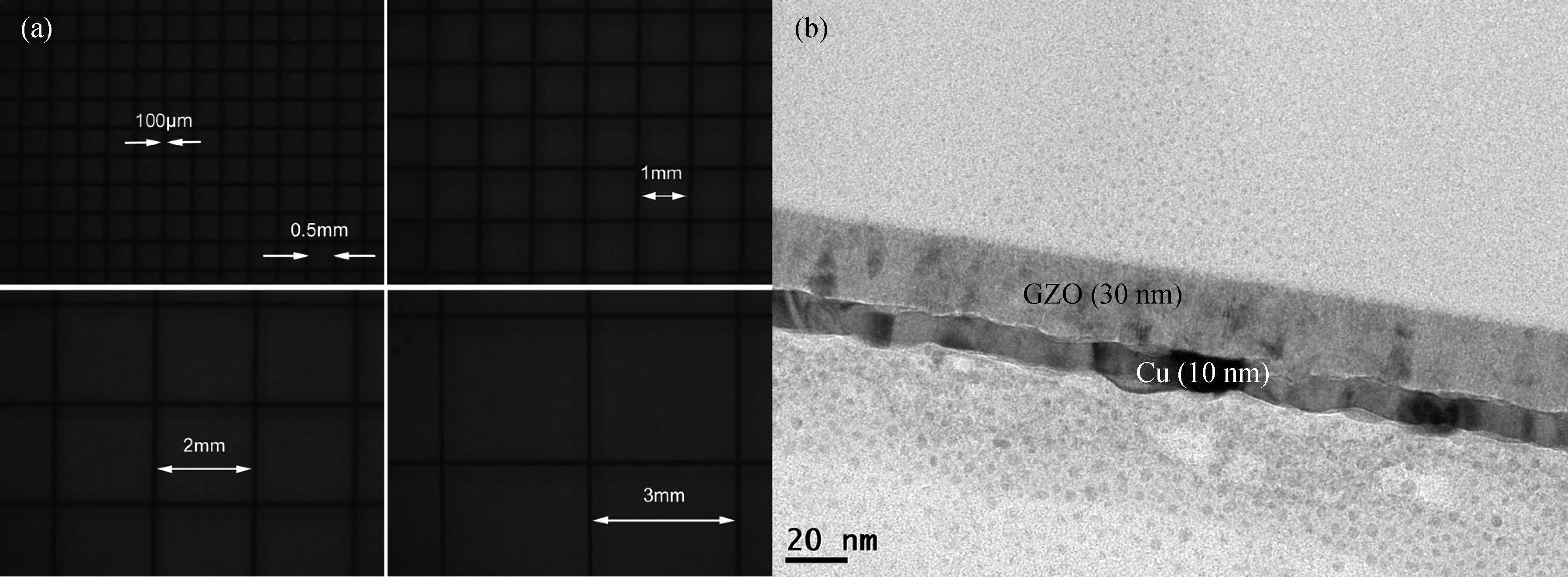
Fig1.
(a) Optical microscopic images of the GZO/Cu grid double layer with various Cu grid spacing distances. (b) TEM cross sectional image of the GZO/Cu grid double layer.
SEMICONDUCTOR MATERIALS
Cholho Jang1, 2, Zhizhen Ye1, and Jianguo Lü1
Corresponding author: Ye Zhizhen,Email:yezz@zju.edu.cn
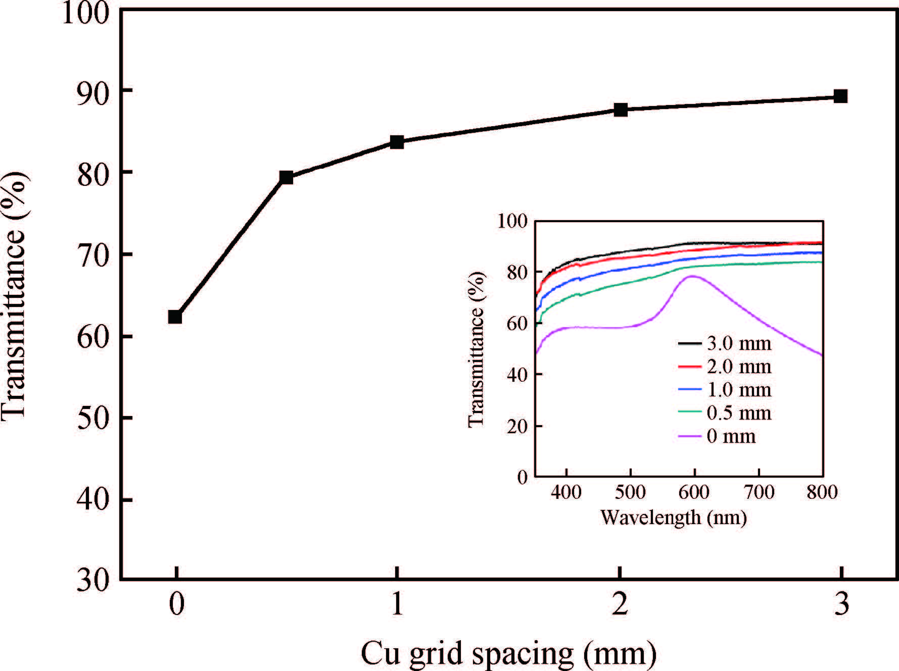
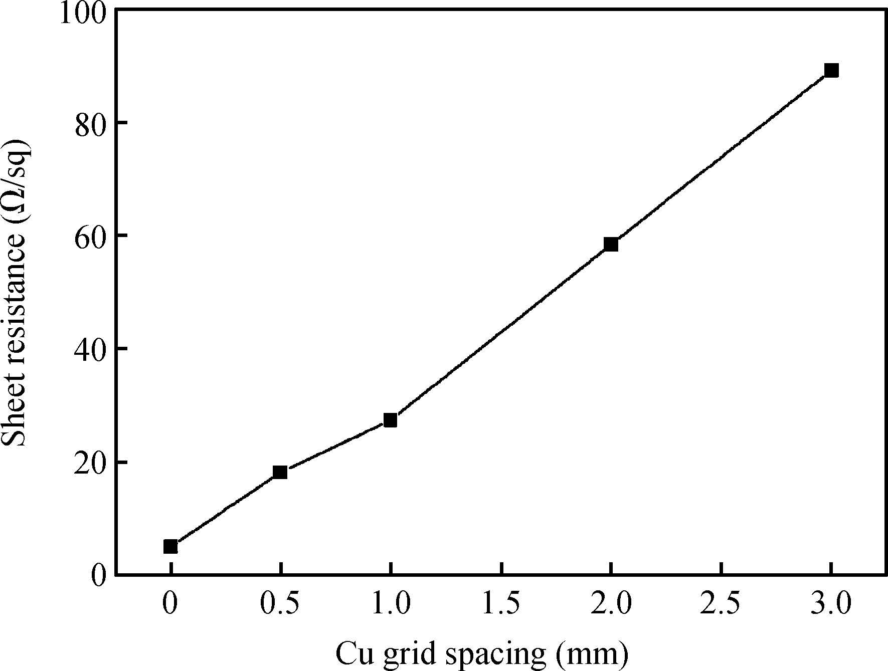
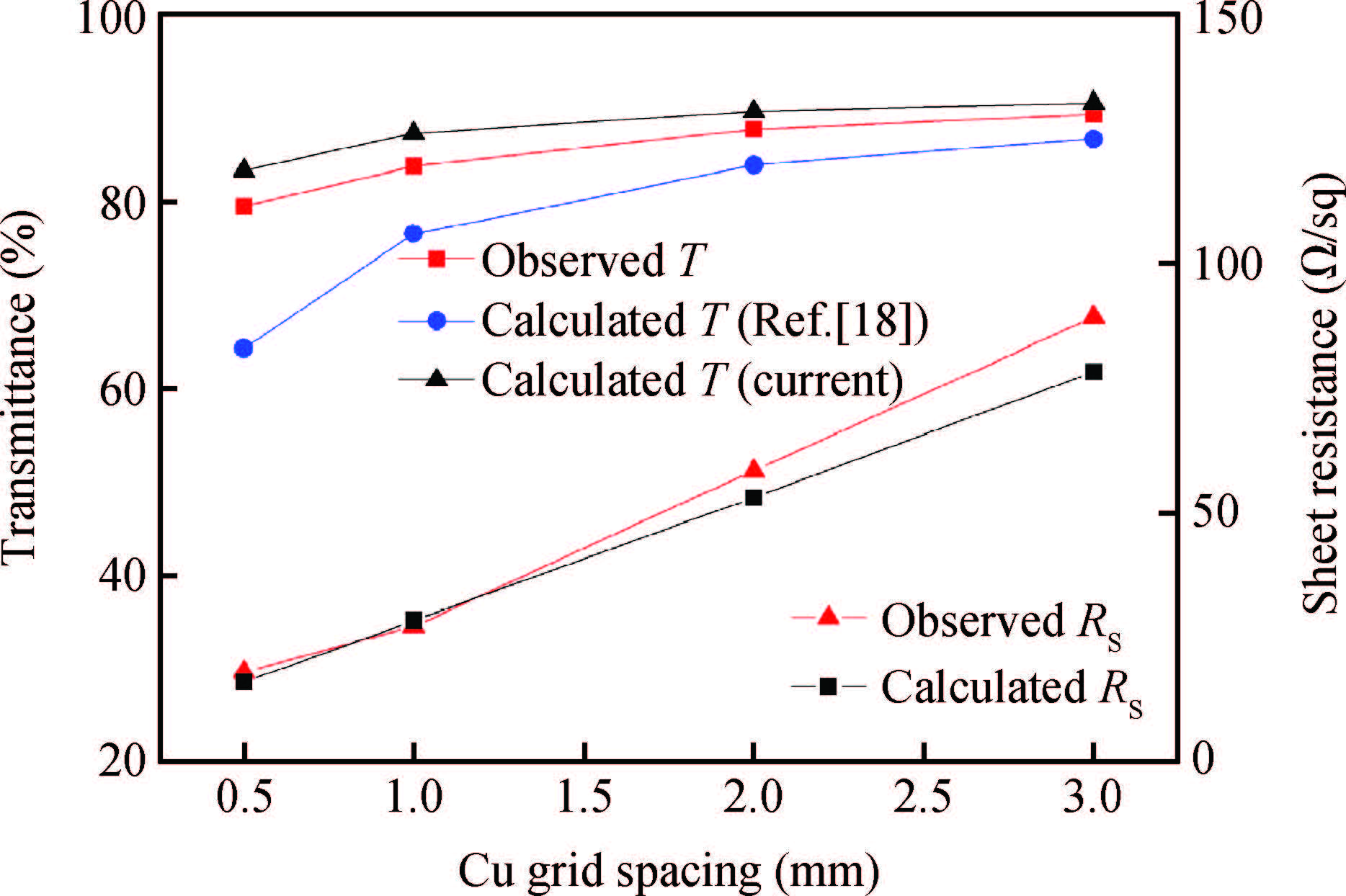
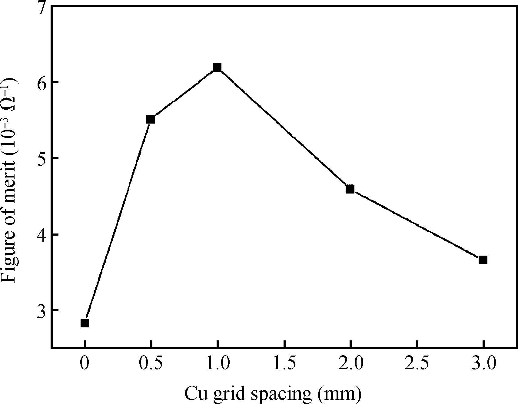
Abstract: Ga doped ZnO(GZO)/Cu grid double layer structures were prepared at room temperature(RT). We have studied the electrical and optical characteristics of the GZO/Cu grid double layer as a function of the Cu grid spacing distance. The optical transmittance and sheet resistance of the GZO/Cu grid double layer are higher than that of the GZO/Cu film double layer regardless of the Cu grid spacing distance and increase as the Cu grid spacing distance increases. The calculated values for the transmittance and sheet resistance of the GZO/Cu grid double layer well follow the trend of the experimentally observed transmittance and sheet resistance ones. For the GZO/Cu grid double layer with a Cu grid spacing distance of 1 mm, the highest figure of merit(ΦTC=6.19×10⁻³ Ω-1) was obtained. In this case, the transmittance, resistivity and filling factor(FF) of the GZO/Cu grid double layer are 83.74%, 1.10×10⁻⁴ Ω·cm and 0.173, respectively.
Key words: transparent electrode, electron beam evaporation, Cu grid, Ga doped ZnO
| [1] | |
| [2] | |
| [3] | |
| [4] | |
| [5] | |
| [6] | |
| [7] | |
| [8] | |
| [9] | |
| [10] | |
| [11] | |
| [12] | |
| [13] | |
| [14] | |
| [15] | |
| [16] | |
| [17] | |
| [18] | |
| [19] | |
| [20] | |
| [21] |
| [1] | |
| [2] | |
| [3] | |
| [4] | |
| [5] | |
| [6] | |
| [7] | |
| [8] | |
| [9] | |
| [10] | |
| [11] | |
| [12] | |
| [13] | |
| [14] | |
| [15] | |
| [16] | |
| [17] | |
| [18] | |
| [19] | |
| [20] | |
| [21] |


Article views: 2861 Times PDF downloads: 10 Times Cited by: 0 Times
Received: 05 May 2015 Revised: Online: Published: 01 December 2015
| Citation: |
Cholho Jang, Zhizhen Ye, Jianguo Lü. Highly transparent low resistance Ga doped ZnO/Cu grid double layers prepared at room temperature[J]. Journal of Semiconductors, 2015, 36(12): 123003. doi: 10.1088/1674-4926/36/12/123003
****
C Jang, Z Z Ye, J Lü. Highly transparent low resistance Ga doped ZnO/Cu grid double layers prepared at room temperature[J]. J. Semicond., 2015, 36(12): 123003. doi: 10.1088/1674-4926/36/12/123003.

|
Project supported by the Key Project of the National Natural Science Foundation of China(No. 91333203), the Program for Innovative Research Team in University of Ministry of Education of China(No. IRT13037), the National Natural Science Foundation of China(No. 51172204), and the Zhejiang Provincial Department of Science and Technology of China(No. 2010R50020).
| [1] | |
| [2] | |
| [3] | |
| [4] | |
| [5] | |
| [6] | |
| [7] | |
| [8] | |
| [9] | |
| [10] | |
| [11] | |
| [12] | |
| [13] | |
| [14] | |
| [15] | |
| [16] | |
| [17] | |
| [18] | |
| [19] | |
| [20] | |
| [21] |

 WeChat ID
Journal of Semiconductors © 2017 All Rights Reserved 京ICP備05085259號-2
 DownLoad:

