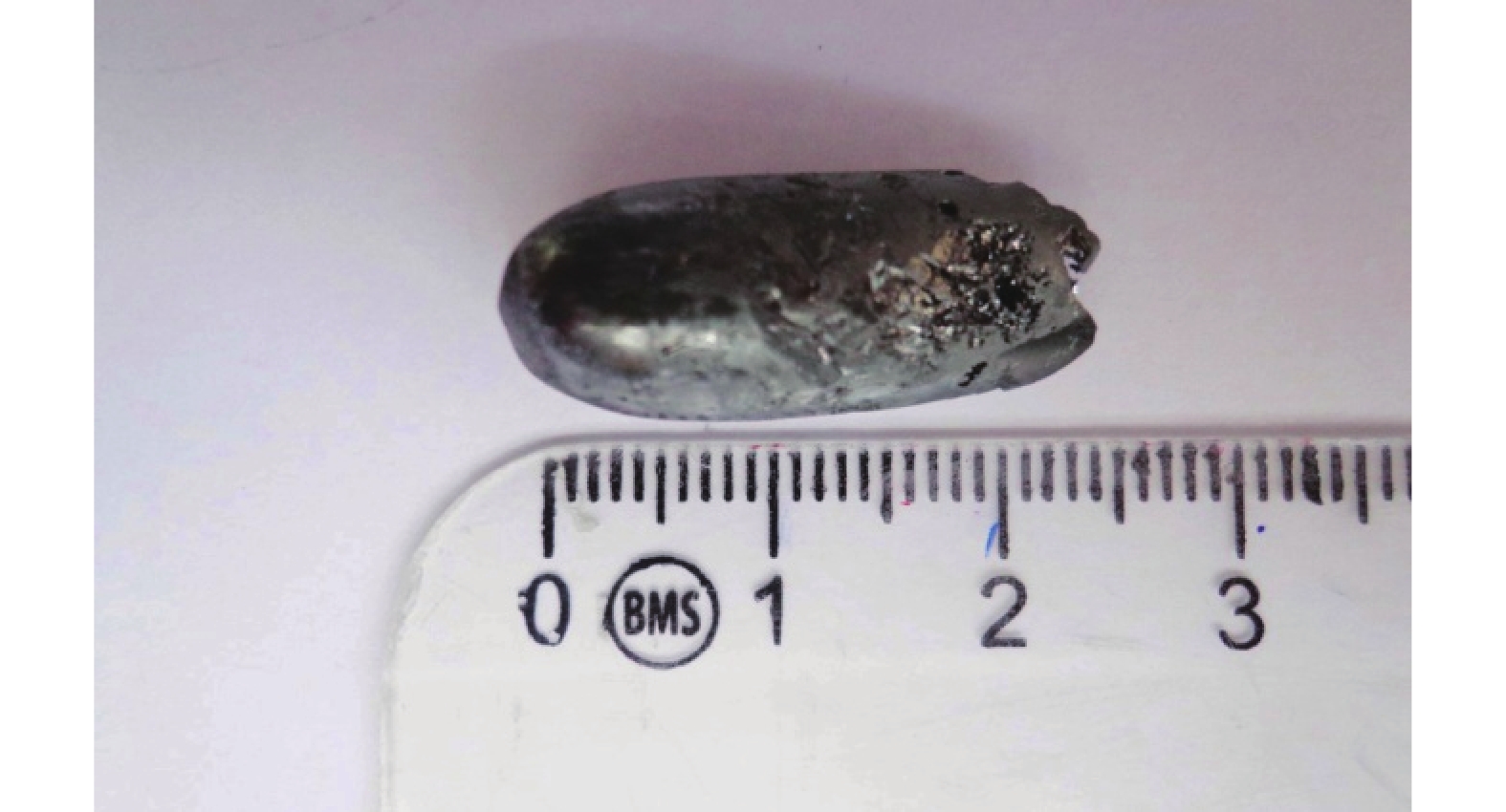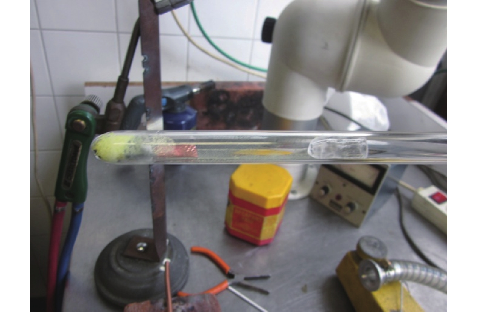
Fig. 1.
The ampoule containing the constituent elements of CZTS under evacuation.
ARTICLES
S. Kerour1, 2, A. Bouloufa1, 2, , M. Lasladj1, 2, K. Djessas3 and K. Medjnoun3
Corresponding author: A. Bouloufa, abdeslam_bouloufa@yahoo.fr
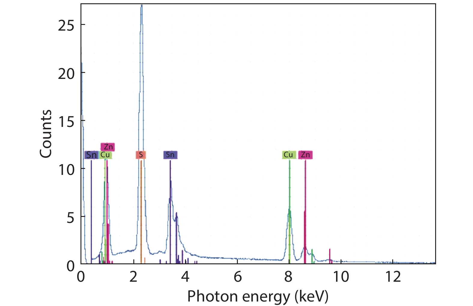
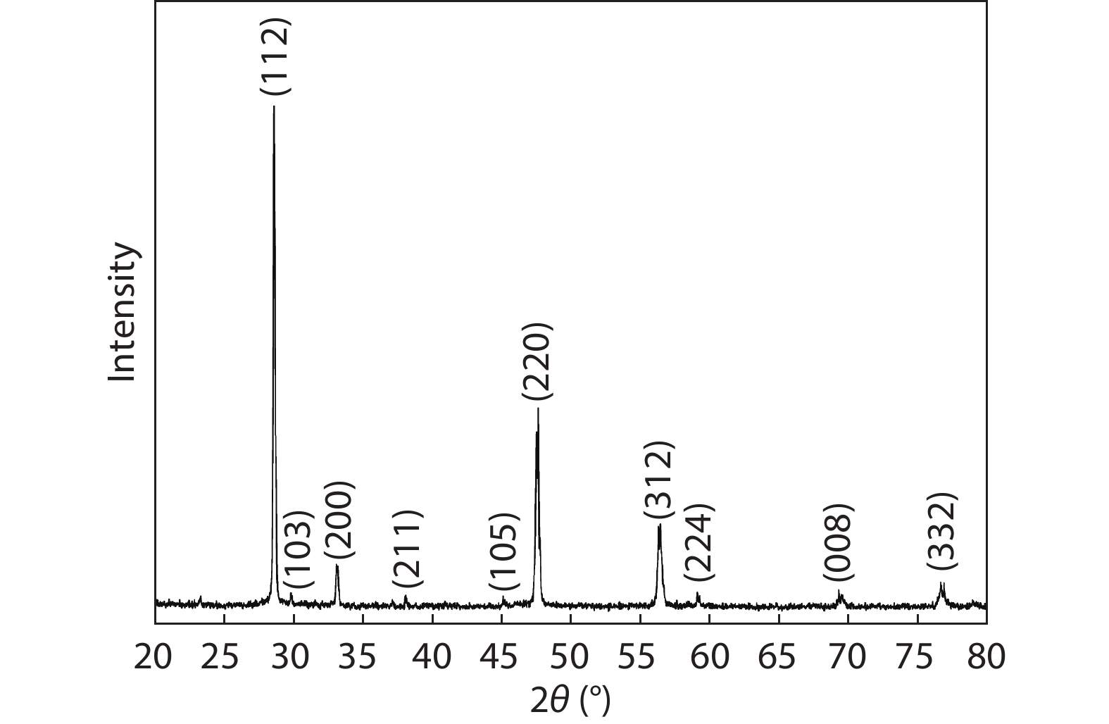
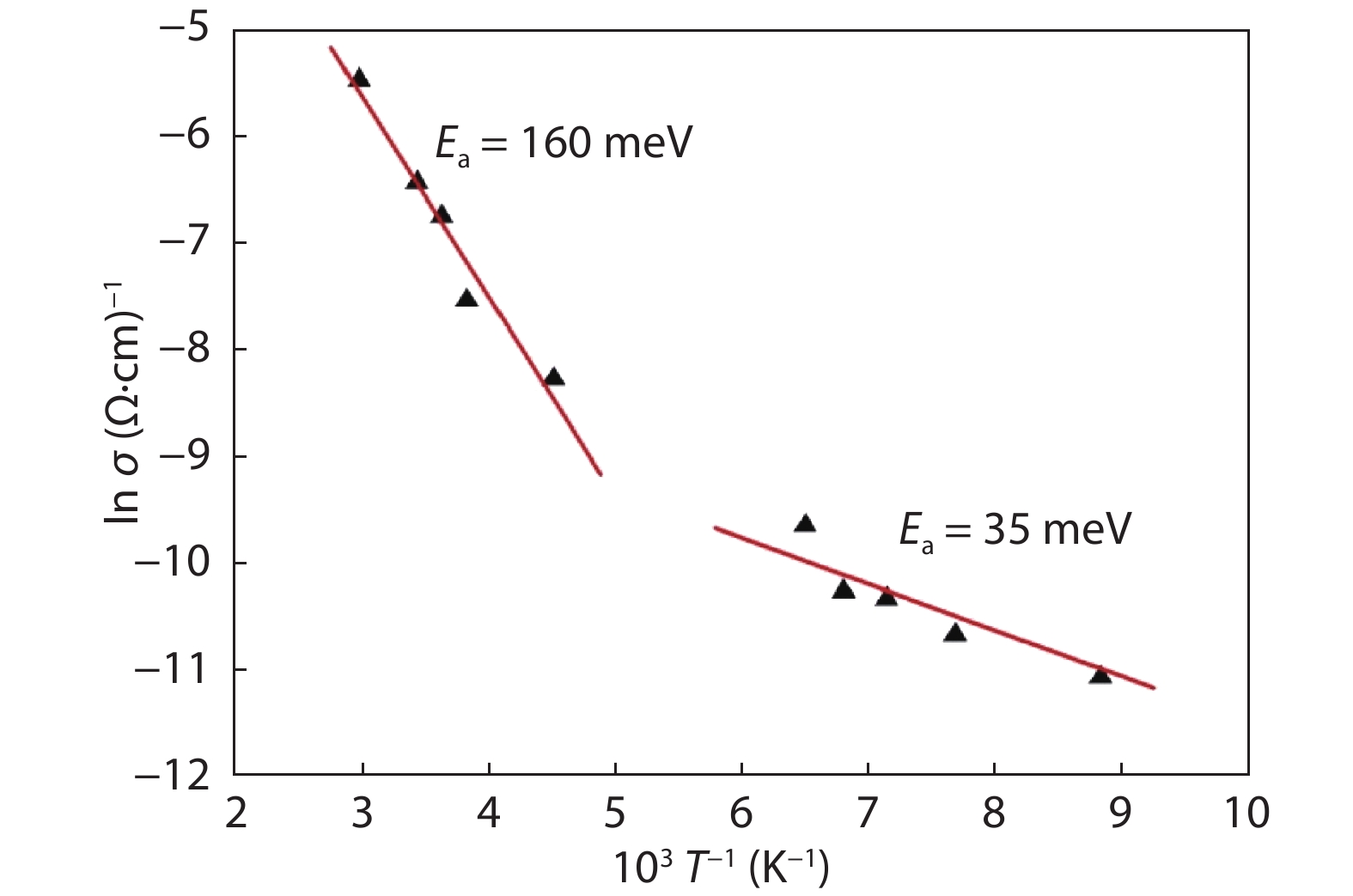
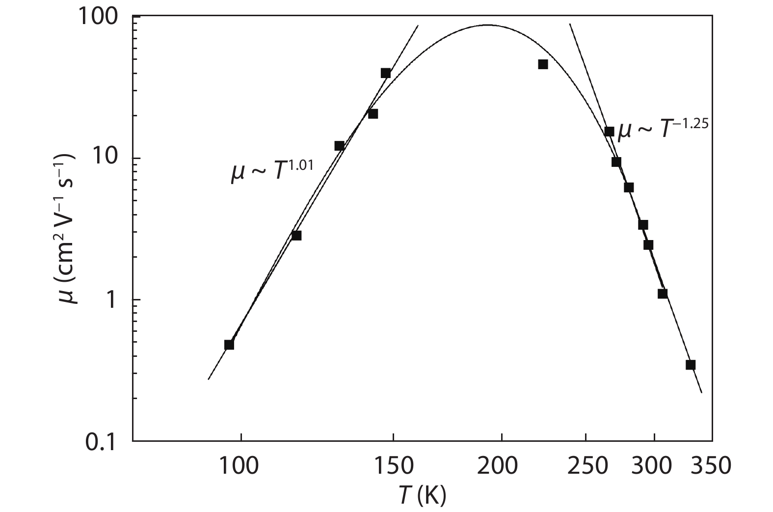
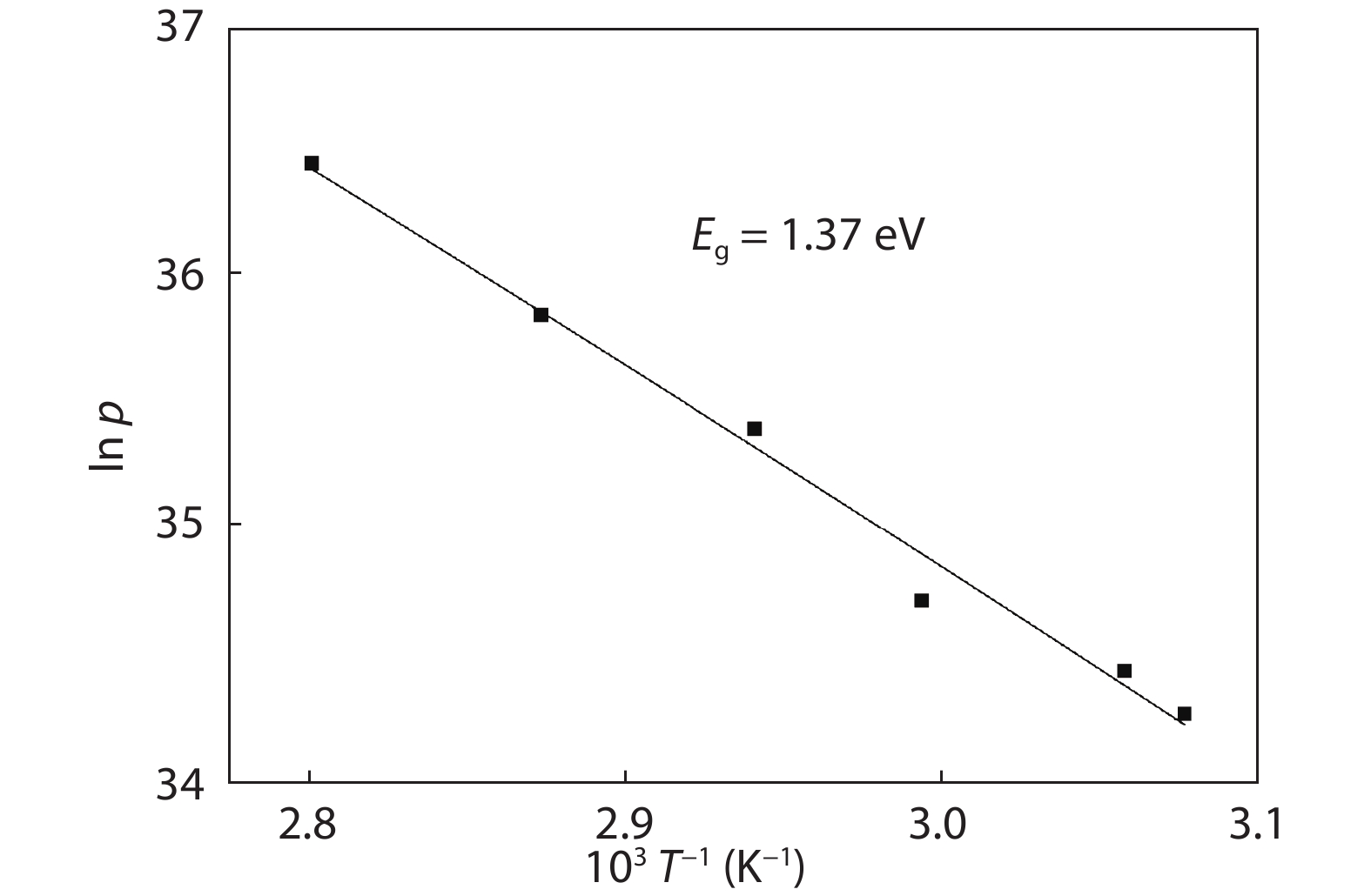
Abstract: In this work, a Cu2ZnSnS4 (CZTS) ingot is grown via a melting method, then cooled; the resulting molten stoichiometric mixture is sealed off in a quartz ampoule under vacuum. The CZTS powder chemical composition analyses are determined using energy dispersive spectroscopy, and revealing the slightly Cu-rich and Zn-poor character of the ingot. Powder X-ray diffraction analysis reveals a crystalline structure with a kesterite phase formation, and a preferred orientation of (112) plane. The lattice constants of the a- and c- axes, calculated based on the XRD analyses, are a = 5.40 ? and c = 10.84 ?. Based on Hall measurements at room temperature, we find that the crystal exhibits p-type conductivity, with a high concentration of 1018 cm–3, a resistivity of 1.7 Ω cm, and a mobility of 10.69 cm2V–1s–1. Activation energies are estimated based on an Arrhenius plot of conductivity versus 1/T, for a temperature range of 80–350 K, measuring 35 and 160 meV in low- and high-temperature regimes, respectively, which is attributed to complex defects (2CuZn+SnZn) and antisite defects (CuZn), respectively. The observed scattering mechanisms are attributed to ionized impurities and acoustic phonons at low and high temperatures, respectively. The extracted band-gap is 1.37 eV.
Key words: Cu2ZnSnS4, growth, melting method, kesterite, Hall measurements
| [1] |
Owusu P A, Asumadu-Sarkodie S. A review of renewable energy sources, sustainability issues and climate change mitigation. Cogent Eng, 2016, 3, 1167990 doi: 10.1080/23311916.2016.1167990
|
| [2] |
Kato T, Wu J L, Hirai Y, et al. Record efficiency for thin-film polycrystalline solar cells up to 22.9% achieved by Cs-treated Cu(In, Ga)(Se, S)2. IEEE J Photovolt, 2019, 9, 325 doi: 10.1109/JPHOTOV.2018.2882206
|
| [3] |
Nakamura M, Yamaguchi K, Kimoto Y, et al. Cd-free Cu(In, Ga)(Se, S)2 thin-film solar cell with record efficiency of 23.35%. IEEE J Photovolt, 2019, 9, 1863 doi: 10.1109/JPHOTOV.2019.2937218
|
| [4] |
Candelise C, Winskel M, Gross R. Implications for CdTe and CIGS technologies production costs of indium and tellurium scarcity. Prog Photovolt: Res Appl, 2012, 20, 816 doi: 10.1002/pip.2216
|
| [5] |
Wadia C, Alivisatos A P, Kammen D M. Materials availability expands the opportunity for large-scale photovoltaics deployment. Environ Sci Technol, 2009, 43, 2072 doi: 10.1021/es8019534
|
| [6] |
Terlemezoglu M, Bayrakl? Sürücü ?, Dogru C, et al. CZTSSe thin films fabricated by single step deposition for superstrate solar cell applications. J Mater Sci: Mater Electron, 2019, 30, 11301 doi: 10.1007/s10854-019-01477-9
|
| [7] |
Lai F I, Yang J F, Wei Y L, et al. High quality sustainable Cu2ZnSnSe4 (CZTSe) absorber layers in highly efficient CZTSe solar cells. Green Chem, 2017, 19, 795 doi: 10.1039/C6GC02300B
|
| [8] |
Paranthaman M P, Wong-Ng W, Bhattacharya R N. Semiconductor materials for solar photovoltaic cells. Cham: Springer International Publishing, 2016
|
| [9] |
Kishore Kumar Y B, Suresh Babu G, Uday Bhaskar P, et al. Preparation and characterization of spray-deposited Cu2ZnSnS4 thin films. Sol Energy Mater Sol Cells, 2009, 93, 1230 doi: 10.1016/j.solmat.2009.01.011
|
| [10] |
Ziti A, Hartiti B, Labrim H, et al. Effect of copper concentration on physical properties of CZTS thin films deposited by dip-coating technique. Appl Phys A, 2019, 125, 1 doi: 10.1007/s00339-019-2513-0
|
| [11] |
Gour K S, Yadav A K, Singh O P, et al. Na incorporated improved properties of Cu2ZnSnS4 (CZTS) thin film by DC sputtering. Vacuum, 2018, 154, 148 doi: 10.1016/j.vacuum.2018.05.007
|
| [12] |
Ito K, Nakazawa T. Electrical and optical properties of stannite-type quaternary semiconductor thin films. Jpn J Appl Phys, 1988, 27, 2094 doi: 10.1143/JJAP.27.2094
|
| [13] |
Katagiri H, Jimbo K, Yamada S, et al. Enhanced conversion efficiencies of Cu2ZnSnS4-based thin film solar cells by using preferential etching technique. Appl Phys Express, 2008, 1, 041201 doi: 10.1143/APEX.1.041201
|
| [14] |
Ito K. Copper zinc tin sulfide-based thin-film solar cells. Chichester, UK: John Wiley & Sons Ltd, 2014
|
| [15] |
Wang W, Winkler M T, Gunawan O, et al. Device characteristics of CZTSSe thin-film solar cells with 12.6% efficiency. Adv Energy Mater, 2014, 4, 1301465 doi: 10.1002/aenm.201301465
|
| [16] |
Shockley W, Queisser H J. Detailed balance limit of efficiency of p-n junction solar cells. J Appl Phys, 1961, 32, 510 doi: 10.1063/1.1736034
|
| [17] |
Mai D L, Park H J, Choi I H. Growth of Cu2ZnSnS4 crystals by the directional freezing method with an induction heater. J Cryst Growth, 2014, 402, 104 doi: 10.1016/j.jcrysgro.2014.05.014
|
| [18] |
Grossberg M, Krustok J, Raadik T, et al. Photoluminescence study of disordering in the cation sublattice of Cu2ZnSnS4. Curr Appl Phys, 2014, 14, 1424 doi: 10.1016/j.cap.2014.08.013
|
| [19] |
Choubrac L, Lafond A, Guillot-Deudon C, et al. Structure flexibility of the Cu2ZnSnS4 absorber in low-cost photovoltaic cells: From the stoichiometric to the copper-poor compounds. Inorg Chem, 2012, 51, 3346 doi: 10.1021/ic202569q
|
| [20] |
Nagaoka A, Yoshino K, Taniguchi H, et al. Growth of Cu2ZnSnS4 single crystal by traveling heater method. Jpn J Appl Phys, 2011, 50, 128001 doi: 10.1143/JJAP.50.128001
|
| [21] |
Nagaoka A, Yoshino K, Taniguchi H, et al. Growth and characterization of Cu2ZnSnS4 single crystals. Phys Status Solidi A, 2013, 210, 1328 doi: 10.1002/pssa.201200815
|
| [22] |
Das S, Krishna R M, Ma S G, et al. Single phase polycrystalline Cu2ZnSnS4 grown by vertical gradient freeze technique. J Cryst Growth, 2013, 381, 148 doi: 10.1016/j.jcrysgro.2013.07.022
|
| [23] |
Ben Marai A, Ben Belgacem J, Ben Ayadi Z, et al. Structural and optical properties of CuIn1– xGaxSe2 nanoparticles synthesized by solvothermal route. J Alloy Compd, 2016, 658, 961 doi: 10.1016/j.jallcom.2015.10.287
|
| [24] |
Lahlali S, Belaqziz M, Amhil S, et al. Structural, optical and electrical properties of CuIn0.7Ga0.3Se2 ingot prepared by direct melting. J Electron Mater, 2020, 49, 7518 doi: 10.1007/s11664-020-08463-6
|
| [25] |
Sagna A, Djessas K, Sene C, et al. Close spaced vapor transport deposition of Cu2ZnSnS4 thin films: Effect of iodine pressure. J Alloy Compd, 2016, 685, 699 doi: 10.1016/j.jallcom.2016.05.297
|
| [26] |
Tomlinson R D. Fabrication of CuInSe2 single crystals using melt-growth techniques. Sol Cells, 1986, 16, 17 doi: 10.1016/0379-6787(86)90072-4
|
| [27] |
Peng D Y, Zhao J J. Representation of the vapour pressures of sulfur. J Chem Thermodyn, 2001, 33, 1121 doi: 10.1006/jcht.2001.0835
|
| [28] |
Sagna A. Etude et élaboration par close-spaced vapor transport (CSVT), d’absorbeurs Cu2ZnSnS4 en couches minces polycristallines destinées à la réalisation de photopiles à faible co?t. PhD Dissertation, Université Perpignan, 2016 (in French)
|
| [29] |
Shah J S. Growth, morphology and impurity characterisation of some I III IV2 sulphides and selenides. Prog Cryst Growth Charact, 1980, 3, 333 doi: 10.1016/0146-3535(80)90005-2
|
| [30] |
Atkins P W, De Paula J. Physical chemistry for the life sciences. Oxford: Oxford University Press, 2011
|
| [31] |
Sharma R C, Chang Y A. The S?Sn (sulfur-tin) system. Bull Alloy Phase Diagrams, 1986, 7, 269 doi: 10.1007/BF02869004
|
| [32] |
Sharma K C, Chang Y A. The S-Zn (sulfur-zinc) system. J Phase Equilibria, 1996, 17, 261 doi: 10.1007/BF02648496
|
| [33] |
Chakrabarti D J, Laughlin D E. The Cu-S (copper-sulfur) system. Bull Alloy Phase Diagrams, 1983, 4, 254 doi: 10.1007/BF02868665
|
| [34] |
Hergert F, Hock R. Predicted formation reactions for the solid-state syntheses of the semiconductor materials Cu2SnX3 and Cu2ZnSnX4 (X = S, Se) starting from binary chalcogenides. Thin Solid Films, 2007, 515, 5953 doi: 10.1016/j.tsf.2006.12.096
|
| [35] |
Chen S Y, Walsh A, Gong X G, et al. Classification of lattice defects in the kesterite Cu2ZnSnS4 and Cu2ZnSnSe4 earth-abundant solar cell absorbers. Adv Mater, 2013, 25, 1522 doi: 10.1002/adma.201203146
|
| [36] |
Olekseyuk I D, Dudchak I V, Piskach L V. Phase equilibria in the Cu2S-ZnS-SnS2 system. J Alloy Compd, 2004, 368, 135 doi: 10.1016/j.jallcom.2003.08.084
|
| [37] |
Wojdyr M. Fityk: a general-purpose peak fitting program. J Appl Crystallogr, 2010, 43, 1126 doi: 10.1107/S0021889810030499
|
| [38] |
Katagiri H, Ishigaki N, Ishida T, et al. Characterization of Cu2ZnSnS4 thin films prepared by vapor phase sulfurization. Jpn J Appl Phys, 2001, 40, 500 doi: 10.1143/JJAP.40.500
|
| [39] |
Nakayama N, Ito K. Sprayed films of stannite Cu2ZnSnS4. Appl Surf Sci, 1996, 92, 171 doi: 10.1016/0169-4332(95)00225-1
|
| [40] |
Tanaka T, Sueishi T, Saito K, et al. Existence and removal of Cu2Se second phase in coevaporated Cu2ZnSnSe4 thin films. J Appl Phys, 2012, 111, 053522 doi: 10.1063/1.3691964
|
| [41] |
Nagaoka A, Katsube R, Nakatsuka S, et al. Growth and characterization of Cu2ZnSn(SxSe1? x)4 single crystal grown by traveling heater method. J Cryst Growth, 2015, 423, 9 doi: 10.1016/j.jcrysgro.2015.04.012
|
| [42] |
Nagaoka A, Scarpulla M A, Yoshino K. Na-doped Cu2ZnSnS4 single crystal grown by traveling-heater method. J Cryst Growth, 2016, 453, 119 doi: 10.1016/j.jcrysgro.2016.08.014
|
| [43] |
Petritz R L. Theory of photoconductivity in semiconductor films. Phys Rev, 1956, 104, 1508 doi: 10.1103/PhysRev.104.1508
|
| [44] |
Blatt F J. Scattering of carriers by ionized impurities in semiconductors. J Phys Chem Solids, 1957, 1, 262 doi: 10.1016/0022-3697(57)90014-8
|
| [45] |
Debye P P, Conwell E M. Electrical properties of N-type germanium. Phys Rev, 1954, 93, 693 doi: 10.1103/PhysRev.93.693
|
Table 1. Chemical composition of CZTS.
| Atomic composition (%) | Cu/(Zn+Sn) | Zn/Sn | ||||
| Cu | Zn | Sn | S | |||
| Point 1 | 31.61 | 11.68 | 12.88 | 43.83 | 1.28 | 0.9 |
| Point 2 | 27.73 | 10.24 | 12.07 | 49.96 | 1.24 | 0.85 |
| Average | 29.67 | 10.96 | 12.47 | 46.89 | 1.26 | 0.88 |
 DownLoad: CSV
| [1] |
Owusu P A, Asumadu-Sarkodie S. A review of renewable energy sources, sustainability issues and climate change mitigation. Cogent Eng, 2016, 3, 1167990 doi: 10.1080/23311916.2016.1167990
|
| [2] |
Kato T, Wu J L, Hirai Y, et al. Record efficiency for thin-film polycrystalline solar cells up to 22.9% achieved by Cs-treated Cu(In, Ga)(Se, S)2. IEEE J Photovolt, 2019, 9, 325 doi: 10.1109/JPHOTOV.2018.2882206
|
| [3] |
Nakamura M, Yamaguchi K, Kimoto Y, et al. Cd-free Cu(In, Ga)(Se, S)2 thin-film solar cell with record efficiency of 23.35%. IEEE J Photovolt, 2019, 9, 1863 doi: 10.1109/JPHOTOV.2019.2937218
|
| [4] |
Candelise C, Winskel M, Gross R. Implications for CdTe and CIGS technologies production costs of indium and tellurium scarcity. Prog Photovolt: Res Appl, 2012, 20, 816 doi: 10.1002/pip.2216
|
| [5] |
Wadia C, Alivisatos A P, Kammen D M. Materials availability expands the opportunity for large-scale photovoltaics deployment. Environ Sci Technol, 2009, 43, 2072 doi: 10.1021/es8019534
|
| [6] |
Terlemezoglu M, Bayrakl? Sürücü ?, Dogru C, et al. CZTSSe thin films fabricated by single step deposition for superstrate solar cell applications. J Mater Sci: Mater Electron, 2019, 30, 11301 doi: 10.1007/s10854-019-01477-9
|
| [7] |
Lai F I, Yang J F, Wei Y L, et al. High quality sustainable Cu2ZnSnSe4 (CZTSe) absorber layers in highly efficient CZTSe solar cells. Green Chem, 2017, 19, 795 doi: 10.1039/C6GC02300B
|
| [8] |
Paranthaman M P, Wong-Ng W, Bhattacharya R N. Semiconductor materials for solar photovoltaic cells. Cham: Springer International Publishing, 2016
|
| [9] |
Kishore Kumar Y B, Suresh Babu G, Uday Bhaskar P, et al. Preparation and characterization of spray-deposited Cu2ZnSnS4 thin films. Sol Energy Mater Sol Cells, 2009, 93, 1230 doi: 10.1016/j.solmat.2009.01.011
|
| [10] |
Ziti A, Hartiti B, Labrim H, et al. Effect of copper concentration on physical properties of CZTS thin films deposited by dip-coating technique. Appl Phys A, 2019, 125, 1 doi: 10.1007/s00339-019-2513-0
|
| [11] |
Gour K S, Yadav A K, Singh O P, et al. Na incorporated improved properties of Cu2ZnSnS4 (CZTS) thin film by DC sputtering. Vacuum, 2018, 154, 148 doi: 10.1016/j.vacuum.2018.05.007
|
| [12] |
Ito K, Nakazawa T. Electrical and optical properties of stannite-type quaternary semiconductor thin films. Jpn J Appl Phys, 1988, 27, 2094 doi: 10.1143/JJAP.27.2094
|
| [13] |
Katagiri H, Jimbo K, Yamada S, et al. Enhanced conversion efficiencies of Cu2ZnSnS4-based thin film solar cells by using preferential etching technique. Appl Phys Express, 2008, 1, 041201 doi: 10.1143/APEX.1.041201
|
| [14] |
Ito K. Copper zinc tin sulfide-based thin-film solar cells. Chichester, UK: John Wiley & Sons Ltd, 2014
|
| [15] |
Wang W, Winkler M T, Gunawan O, et al. Device characteristics of CZTSSe thin-film solar cells with 12.6% efficiency. Adv Energy Mater, 2014, 4, 1301465 doi: 10.1002/aenm.201301465
|
| [16] |
Shockley W, Queisser H J. Detailed balance limit of efficiency of p-n junction solar cells. J Appl Phys, 1961, 32, 510 doi: 10.1063/1.1736034
|
| [17] |
Mai D L, Park H J, Choi I H. Growth of Cu2ZnSnS4 crystals by the directional freezing method with an induction heater. J Cryst Growth, 2014, 402, 104 doi: 10.1016/j.jcrysgro.2014.05.014
|
| [18] |
Grossberg M, Krustok J, Raadik T, et al. Photoluminescence study of disordering in the cation sublattice of Cu2ZnSnS4. Curr Appl Phys, 2014, 14, 1424 doi: 10.1016/j.cap.2014.08.013
|
| [19] |
Choubrac L, Lafond A, Guillot-Deudon C, et al. Structure flexibility of the Cu2ZnSnS4 absorber in low-cost photovoltaic cells: From the stoichiometric to the copper-poor compounds. Inorg Chem, 2012, 51, 3346 doi: 10.1021/ic202569q
|
| [20] |
Nagaoka A, Yoshino K, Taniguchi H, et al. Growth of Cu2ZnSnS4 single crystal by traveling heater method. Jpn J Appl Phys, 2011, 50, 128001 doi: 10.1143/JJAP.50.128001
|
| [21] |
Nagaoka A, Yoshino K, Taniguchi H, et al. Growth and characterization of Cu2ZnSnS4 single crystals. Phys Status Solidi A, 2013, 210, 1328 doi: 10.1002/pssa.201200815
|
| [22] |
Das S, Krishna R M, Ma S G, et al. Single phase polycrystalline Cu2ZnSnS4 grown by vertical gradient freeze technique. J Cryst Growth, 2013, 381, 148 doi: 10.1016/j.jcrysgro.2013.07.022
|
| [23] |
Ben Marai A, Ben Belgacem J, Ben Ayadi Z, et al. Structural and optical properties of CuIn1– xGaxSe2 nanoparticles synthesized by solvothermal route. J Alloy Compd, 2016, 658, 961 doi: 10.1016/j.jallcom.2015.10.287
|
| [24] |
Lahlali S, Belaqziz M, Amhil S, et al. Structural, optical and electrical properties of CuIn0.7Ga0.3Se2 ingot prepared by direct melting. J Electron Mater, 2020, 49, 7518 doi: 10.1007/s11664-020-08463-6
|
| [25] |
Sagna A, Djessas K, Sene C, et al. Close spaced vapor transport deposition of Cu2ZnSnS4 thin films: Effect of iodine pressure. J Alloy Compd, 2016, 685, 699 doi: 10.1016/j.jallcom.2016.05.297
|
| [26] |
Tomlinson R D. Fabrication of CuInSe2 single crystals using melt-growth techniques. Sol Cells, 1986, 16, 17 doi: 10.1016/0379-6787(86)90072-4
|
| [27] |
Peng D Y, Zhao J J. Representation of the vapour pressures of sulfur. J Chem Thermodyn, 2001, 33, 1121 doi: 10.1006/jcht.2001.0835
|
| [28] |
Sagna A. Etude et élaboration par close-spaced vapor transport (CSVT), d’absorbeurs Cu2ZnSnS4 en couches minces polycristallines destinées à la réalisation de photopiles à faible co?t. PhD Dissertation, Université Perpignan, 2016 (in French)
|
| [29] |
Shah J S. Growth, morphology and impurity characterisation of some I III IV2 sulphides and selenides. Prog Cryst Growth Charact, 1980, 3, 333 doi: 10.1016/0146-3535(80)90005-2
|
| [30] |
Atkins P W, De Paula J. Physical chemistry for the life sciences. Oxford: Oxford University Press, 2011
|
| [31] |
Sharma R C, Chang Y A. The S?Sn (sulfur-tin) system. Bull Alloy Phase Diagrams, 1986, 7, 269 doi: 10.1007/BF02869004
|
| [32] |
Sharma K C, Chang Y A. The S-Zn (sulfur-zinc) system. J Phase Equilibria, 1996, 17, 261 doi: 10.1007/BF02648496
|
| [33] |
Chakrabarti D J, Laughlin D E. The Cu-S (copper-sulfur) system. Bull Alloy Phase Diagrams, 1983, 4, 254 doi: 10.1007/BF02868665
|
| [34] |
Hergert F, Hock R. Predicted formation reactions for the solid-state syntheses of the semiconductor materials Cu2SnX3 and Cu2ZnSnX4 (X = S, Se) starting from binary chalcogenides. Thin Solid Films, 2007, 515, 5953 doi: 10.1016/j.tsf.2006.12.096
|
| [35] |
Chen S Y, Walsh A, Gong X G, et al. Classification of lattice defects in the kesterite Cu2ZnSnS4 and Cu2ZnSnSe4 earth-abundant solar cell absorbers. Adv Mater, 2013, 25, 1522 doi: 10.1002/adma.201203146
|
| [36] |
Olekseyuk I D, Dudchak I V, Piskach L V. Phase equilibria in the Cu2S-ZnS-SnS2 system. J Alloy Compd, 2004, 368, 135 doi: 10.1016/j.jallcom.2003.08.084
|
| [37] |
Wojdyr M. Fityk: a general-purpose peak fitting program. J Appl Crystallogr, 2010, 43, 1126 doi: 10.1107/S0021889810030499
|
| [38] |
Katagiri H, Ishigaki N, Ishida T, et al. Characterization of Cu2ZnSnS4 thin films prepared by vapor phase sulfurization. Jpn J Appl Phys, 2001, 40, 500 doi: 10.1143/JJAP.40.500
|
| [39] |
Nakayama N, Ito K. Sprayed films of stannite Cu2ZnSnS4. Appl Surf Sci, 1996, 92, 171 doi: 10.1016/0169-4332(95)00225-1
|
| [40] |
Tanaka T, Sueishi T, Saito K, et al. Existence and removal of Cu2Se second phase in coevaporated Cu2ZnSnSe4 thin films. J Appl Phys, 2012, 111, 053522 doi: 10.1063/1.3691964
|
| [41] |
Nagaoka A, Katsube R, Nakatsuka S, et al. Growth and characterization of Cu2ZnSn(SxSe1? x)4 single crystal grown by traveling heater method. J Cryst Growth, 2015, 423, 9 doi: 10.1016/j.jcrysgro.2015.04.012
|
| [42] |
Nagaoka A, Scarpulla M A, Yoshino K. Na-doped Cu2ZnSnS4 single crystal grown by traveling-heater method. J Cryst Growth, 2016, 453, 119 doi: 10.1016/j.jcrysgro.2016.08.014
|
| [43] |
Petritz R L. Theory of photoconductivity in semiconductor films. Phys Rev, 1956, 104, 1508 doi: 10.1103/PhysRev.104.1508
|
| [44] |
Blatt F J. Scattering of carriers by ionized impurities in semiconductors. J Phys Chem Solids, 1957, 1, 262 doi: 10.1016/0022-3697(57)90014-8
|
| [45] |
Debye P P, Conwell E M. Electrical properties of N-type germanium. Phys Rev, 1954, 93, 693 doi: 10.1103/PhysRev.93.693
|


Article views: 4001 Times PDF downloads: 32 Times Cited by: 0 Times
Received: 02 December 2020 Revised: 20 January 2021 Online: Accepted Manuscript: 31 March 2021Uncorrected proof: 09 April 2021Published: 05 July 2021
| Citation: |
S. Kerour, A. Bouloufa, M. Lasladj, K. Djessas, K. Medjnoun. Structural and electrical characterization of Cu2ZnSnS4 ingot material grown by melting method[J]. Journal of Semiconductors, 2021, 42(7): 072701. doi: 10.1088/1674-4926/42/7/072701
****
S Kerour, A Bouloufa, M Lasladj, K Djessas, K Medjnoun, Structural and electrical characterization of Cu2ZnSnS4 ingot material grown by melting method[J]. J. Semicond., 2021, 42(7): 072701. doi: 10.1088/1674-4926/42/7/072701.

|
| [1] |
Owusu P A, Asumadu-Sarkodie S. A review of renewable energy sources, sustainability issues and climate change mitigation. Cogent Eng, 2016, 3, 1167990 doi: 10.1080/23311916.2016.1167990
|
| [2] |
Kato T, Wu J L, Hirai Y, et al. Record efficiency for thin-film polycrystalline solar cells up to 22.9% achieved by Cs-treated Cu(In, Ga)(Se, S)2. IEEE J Photovolt, 2019, 9, 325 doi: 10.1109/JPHOTOV.2018.2882206
|
| [3] |
Nakamura M, Yamaguchi K, Kimoto Y, et al. Cd-free Cu(In, Ga)(Se, S)2 thin-film solar cell with record efficiency of 23.35%. IEEE J Photovolt, 2019, 9, 1863 doi: 10.1109/JPHOTOV.2019.2937218
|
| [4] |
Candelise C, Winskel M, Gross R. Implications for CdTe and CIGS technologies production costs of indium and tellurium scarcity. Prog Photovolt: Res Appl, 2012, 20, 816 doi: 10.1002/pip.2216
|
| [5] |
Wadia C, Alivisatos A P, Kammen D M. Materials availability expands the opportunity for large-scale photovoltaics deployment. Environ Sci Technol, 2009, 43, 2072 doi: 10.1021/es8019534
|
| [6] |
Terlemezoglu M, Bayrakl? Sürücü ?, Dogru C, et al. CZTSSe thin films fabricated by single step deposition for superstrate solar cell applications. J Mater Sci: Mater Electron, 2019, 30, 11301 doi: 10.1007/s10854-019-01477-9
|
| [7] |
Lai F I, Yang J F, Wei Y L, et al. High quality sustainable Cu2ZnSnSe4 (CZTSe) absorber layers in highly efficient CZTSe solar cells. Green Chem, 2017, 19, 795 doi: 10.1039/C6GC02300B
|
| [8] |
Paranthaman M P, Wong-Ng W, Bhattacharya R N. Semiconductor materials for solar photovoltaic cells. Cham: Springer International Publishing, 2016
|
| [9] |
Kishore Kumar Y B, Suresh Babu G, Uday Bhaskar P, et al. Preparation and characterization of spray-deposited Cu2ZnSnS4 thin films. Sol Energy Mater Sol Cells, 2009, 93, 1230 doi: 10.1016/j.solmat.2009.01.011
|
| [10] |
Ziti A, Hartiti B, Labrim H, et al. Effect of copper concentration on physical properties of CZTS thin films deposited by dip-coating technique. Appl Phys A, 2019, 125, 1 doi: 10.1007/s00339-019-2513-0
|
| [11] |
Gour K S, Yadav A K, Singh O P, et al. Na incorporated improved properties of Cu2ZnSnS4 (CZTS) thin film by DC sputtering. Vacuum, 2018, 154, 148 doi: 10.1016/j.vacuum.2018.05.007
|
| [12] |
Ito K, Nakazawa T. Electrical and optical properties of stannite-type quaternary semiconductor thin films. Jpn J Appl Phys, 1988, 27, 2094 doi: 10.1143/JJAP.27.2094
|
| [13] |
Katagiri H, Jimbo K, Yamada S, et al. Enhanced conversion efficiencies of Cu2ZnSnS4-based thin film solar cells by using preferential etching technique. Appl Phys Express, 2008, 1, 041201 doi: 10.1143/APEX.1.041201
|
| [14] |
Ito K. Copper zinc tin sulfide-based thin-film solar cells. Chichester, UK: John Wiley & Sons Ltd, 2014
|
| [15] |
Wang W, Winkler M T, Gunawan O, et al. Device characteristics of CZTSSe thin-film solar cells with 12.6% efficiency. Adv Energy Mater, 2014, 4, 1301465 doi: 10.1002/aenm.201301465
|
| [16] |
Shockley W, Queisser H J. Detailed balance limit of efficiency of p-n junction solar cells. J Appl Phys, 1961, 32, 510 doi: 10.1063/1.1736034
|
| [17] |
Mai D L, Park H J, Choi I H. Growth of Cu2ZnSnS4 crystals by the directional freezing method with an induction heater. J Cryst Growth, 2014, 402, 104 doi: 10.1016/j.jcrysgro.2014.05.014
|
| [18] |
Grossberg M, Krustok J, Raadik T, et al. Photoluminescence study of disordering in the cation sublattice of Cu2ZnSnS4. Curr Appl Phys, 2014, 14, 1424 doi: 10.1016/j.cap.2014.08.013
|
| [19] |
Choubrac L, Lafond A, Guillot-Deudon C, et al. Structure flexibility of the Cu2ZnSnS4 absorber in low-cost photovoltaic cells: From the stoichiometric to the copper-poor compounds. Inorg Chem, 2012, 51, 3346 doi: 10.1021/ic202569q
|
| [20] |
Nagaoka A, Yoshino K, Taniguchi H, et al. Growth of Cu2ZnSnS4 single crystal by traveling heater method. Jpn J Appl Phys, 2011, 50, 128001 doi: 10.1143/JJAP.50.128001
|
| [21] |
Nagaoka A, Yoshino K, Taniguchi H, et al. Growth and characterization of Cu2ZnSnS4 single crystals. Phys Status Solidi A, 2013, 210, 1328 doi: 10.1002/pssa.201200815
|
| [22] |
Das S, Krishna R M, Ma S G, et al. Single phase polycrystalline Cu2ZnSnS4 grown by vertical gradient freeze technique. J Cryst Growth, 2013, 381, 148 doi: 10.1016/j.jcrysgro.2013.07.022
|
| [23] |
Ben Marai A, Ben Belgacem J, Ben Ayadi Z, et al. Structural and optical properties of CuIn1– xGaxSe2 nanoparticles synthesized by solvothermal route. J Alloy Compd, 2016, 658, 961 doi: 10.1016/j.jallcom.2015.10.287
|
| [24] |
Lahlali S, Belaqziz M, Amhil S, et al. Structural, optical and electrical properties of CuIn0.7Ga0.3Se2 ingot prepared by direct melting. J Electron Mater, 2020, 49, 7518 doi: 10.1007/s11664-020-08463-6
|
| [25] |
Sagna A, Djessas K, Sene C, et al. Close spaced vapor transport deposition of Cu2ZnSnS4 thin films: Effect of iodine pressure. J Alloy Compd, 2016, 685, 699 doi: 10.1016/j.jallcom.2016.05.297
|
| [26] |
Tomlinson R D. Fabrication of CuInSe2 single crystals using melt-growth techniques. Sol Cells, 1986, 16, 17 doi: 10.1016/0379-6787(86)90072-4
|
| [27] |
Peng D Y, Zhao J J. Representation of the vapour pressures of sulfur. J Chem Thermodyn, 2001, 33, 1121 doi: 10.1006/jcht.2001.0835
|
| [28] |
Sagna A. Etude et élaboration par close-spaced vapor transport (CSVT), d’absorbeurs Cu2ZnSnS4 en couches minces polycristallines destinées à la réalisation de photopiles à faible co?t. PhD Dissertation, Université Perpignan, 2016 (in French)
|
| [29] |
Shah J S. Growth, morphology and impurity characterisation of some I III IV2 sulphides and selenides. Prog Cryst Growth Charact, 1980, 3, 333 doi: 10.1016/0146-3535(80)90005-2
|
| [30] |
Atkins P W, De Paula J. Physical chemistry for the life sciences. Oxford: Oxford University Press, 2011
|
| [31] |
Sharma R C, Chang Y A. The S?Sn (sulfur-tin) system. Bull Alloy Phase Diagrams, 1986, 7, 269 doi: 10.1007/BF02869004
|
| [32] |
Sharma K C, Chang Y A. The S-Zn (sulfur-zinc) system. J Phase Equilibria, 1996, 17, 261 doi: 10.1007/BF02648496
|
| [33] |
Chakrabarti D J, Laughlin D E. The Cu-S (copper-sulfur) system. Bull Alloy Phase Diagrams, 1983, 4, 254 doi: 10.1007/BF02868665
|
| [34] |
Hergert F, Hock R. Predicted formation reactions for the solid-state syntheses of the semiconductor materials Cu2SnX3 and Cu2ZnSnX4 (X = S, Se) starting from binary chalcogenides. Thin Solid Films, 2007, 515, 5953 doi: 10.1016/j.tsf.2006.12.096
|
| [35] |
Chen S Y, Walsh A, Gong X G, et al. Classification of lattice defects in the kesterite Cu2ZnSnS4 and Cu2ZnSnSe4 earth-abundant solar cell absorbers. Adv Mater, 2013, 25, 1522 doi: 10.1002/adma.201203146
|
| [36] |
Olekseyuk I D, Dudchak I V, Piskach L V. Phase equilibria in the Cu2S-ZnS-SnS2 system. J Alloy Compd, 2004, 368, 135 doi: 10.1016/j.jallcom.2003.08.084
|
| [37] |
Wojdyr M. Fityk: a general-purpose peak fitting program. J Appl Crystallogr, 2010, 43, 1126 doi: 10.1107/S0021889810030499
|
| [38] |
Katagiri H, Ishigaki N, Ishida T, et al. Characterization of Cu2ZnSnS4 thin films prepared by vapor phase sulfurization. Jpn J Appl Phys, 2001, 40, 500 doi: 10.1143/JJAP.40.500
|
| [39] |
Nakayama N, Ito K. Sprayed films of stannite Cu2ZnSnS4. Appl Surf Sci, 1996, 92, 171 doi: 10.1016/0169-4332(95)00225-1
|
| [40] |
Tanaka T, Sueishi T, Saito K, et al. Existence and removal of Cu2Se second phase in coevaporated Cu2ZnSnSe4 thin films. J Appl Phys, 2012, 111, 053522 doi: 10.1063/1.3691964
|
| [41] |
Nagaoka A, Katsube R, Nakatsuka S, et al. Growth and characterization of Cu2ZnSn(SxSe1? x)4 single crystal grown by traveling heater method. J Cryst Growth, 2015, 423, 9 doi: 10.1016/j.jcrysgro.2015.04.012
|
| [42] |
Nagaoka A, Scarpulla M A, Yoshino K. Na-doped Cu2ZnSnS4 single crystal grown by traveling-heater method. J Cryst Growth, 2016, 453, 119 doi: 10.1016/j.jcrysgro.2016.08.014
|
| [43] |
Petritz R L. Theory of photoconductivity in semiconductor films. Phys Rev, 1956, 104, 1508 doi: 10.1103/PhysRev.104.1508
|
| [44] |
Blatt F J. Scattering of carriers by ionized impurities in semiconductors. J Phys Chem Solids, 1957, 1, 262 doi: 10.1016/0022-3697(57)90014-8
|
| [45] |
Debye P P, Conwell E M. Electrical properties of N-type germanium. Phys Rev, 1954, 93, 693 doi: 10.1103/PhysRev.93.693
|

 WeChat ID
Journal of Semiconductors © 2017 All Rights Reserved 京ICP備05085259號-2