


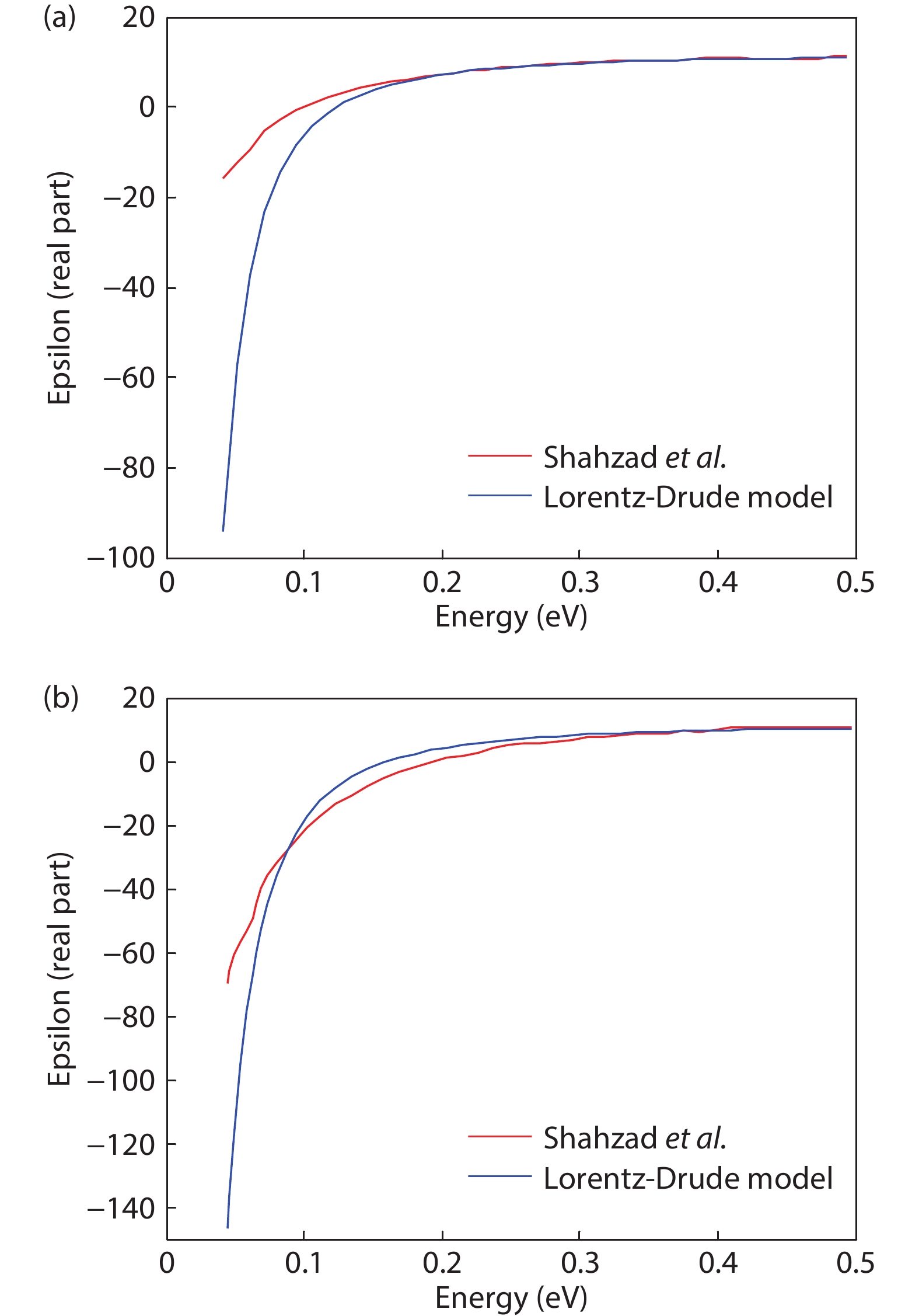
Fig. 1.
(Color online) Comparison between theoretical value and experimental value for carrier concentration of (a) 6 × 1019 cm–3 and (b) 1 × 1020 cm–3.
ARTICLES
Md. Omar Faruque, Rabiul Al Mahmud and Rakibul Hasan Sagor
Corresponding author: Md. Omar Faruque, omarfaruque@iut-dhaka.edu
Abstract: The plasmonic property of heavily doped p-type silicon is studied here. Although most of the plasmonic devices use metal–insulator–metal (MIM) waveguide in order to support the propagation of surface plasmon polaritons (SPPs), metals that possess a number of challenges in loss management, polarization response, nanofabrication etc. On the other hand, heavily doped p-type silicon shows similar plasmonic properties like metals and also enables us to overcome the challenges possessed by metals. For numerical simulation, heavily doped p-silicon is mathematically modeled and the theoretically obtained relative permittivity is compared with the experimental value. A waveguide is formed with the p-silicon-air interface instead of the metal–air interface. Formation and propagation of SPPs similar to MIM waveguides are observed.
Key words: alternative plasmonic material, heavily doped p-silicon, surface plasmon polaritons
| [1] |
Barnes W L, Dereux A, Ebbesen T W. Surface plasmon subwavelength optics. Nature, 2003, 424, 824 doi: 10.1038/nature01937
|
| [2] |
Lu H, Liu X, Wang G, et al. Tunable high-channel-count bandpass plasmonic filters based on an analogue of electromagnetically induced transparency. Nanotechnology, 2012, 23, 444003 doi: 10.1088/0957-4484/23/44/444003
|
| [3] |
Wang H Q, Yang J B, Zhang J J, et al. Tunable band-stop plasmonic waveguide filter with symmetrical multiple-teeth-shaped structure. Opt Lett, 2016, 41, 1233 doi: 10.1364/OL.41.001233
|
| [4] |
Johnson P B, Christy R W. Optical constants of the noble metals. Phys Rev B, 1972, 6, 4370 doi: 10.1103/PhysRevB.6.4370
|
| [5] |
West P R, Ishii S, Naik G V, et al. Searching for better plasmonic materials. Laser Photonics Rev, 2010, 4, 795 doi: 10.1002/lpor.200900055
|
| [6] |
Cai W S, Chettiar U K, Kildishev A V, et al. Optical cloaking with metamaterials. Nat Photonics, 2007, 1, 224 doi: 10.1038/nphoton.2007.28
|
| [7] |
Abelès F, Borensztein Y, López Rios T. Optical properties of discontinuous thin films and rough surfaces of silver. In: Advances in Solid State Physics. Berlin, Heidelberg: Springer Berlin Heidelberg, 2007, 93
|
| [8] |
Berestetskii V B, Lifshitz E M, Pitaevskii L P. Quantum Electrodynamics. Volume 4. Butterworth-Heinemann, 1982
|
| [9] |
Shahzad M, Medhi G, Peale R E, et al. Infrared surface plasmons on heavily doped silicon. J Appl Phys, 2011, 110, 123105 doi: 10.1063/1.3672738
|
| [10] |
Linaschke D, Schilling N, Dani I, et al. Highly n-doped surfaces on n-type silicon wafers by laser-chemical processes. Energy Procedia, 2014, 55, 247 doi: 10.1016/j.egypro.2014.08.076
|
| [11] |
Mizushima I, Murakoshi A, Watanabe M, et al. Hole generation without annealing in high dose boron implanted silicon: Heavy doping by B12 icosahedron as a double acceptor. Jpn J Appl Phys, 1994, 33, 404 doi: 10.1143/JJAP.33.404
|
| [12] |
Vi?a L, Cardona M. Effect of heavy doping on the optical properties and the band structure of silicon. Phys Rev B, 1984, 29, 6739 doi: 10.1103/PhysRevB.29.6739
|
| [13] |
Ma Z, Liu Y, Deng L, et al. Heavily boron-doped silicon layer for the fabrication of nanoscale thermoelectric devices. Nanomaterials, 2018, 8, 77 doi: 10.3390/nano8020077
|
| [14] |
Miyao M, Motooka T, Natsuaki N, et al. Change of the electron effective mass in extremely heavily doped n-type Si obtained by ion implantation and laser annealing. Solid State Commun, 1981, 37, 605 doi: 10.1016/0038-1098(81)90144-7
|
| [15] |
Jellison G E, Modine F A, White C W, et al. Optical properties of heavily doped silicon between 1.5 and 4.1 eV. Phys Rev Lett, 1981, 46, 1414 doi: 10.1103/PhysRevLett.46.1414
|
| [16] |
Nobili, Solmi, Parisini, et al. Precipitation, aggregation, and diffusion in heavily arsenic-doped silicon. Phys Rev B, 1994, 49, 2477 doi: 10.1103/PhysRevB.49.2477
|
| [17] |
Maier S A. Spectroscopy and sensing. In: Plasmonics: Fundamentals and Applications. New York, NY: Springer US, 2007, 177
|
| [18] |
Saber M G, Abadía N, Plant D V. CMOS compatible all-silicon TM pass polarizer based on highly doped silicon waveguide. Opt Express, 2018, 26, 20878 doi: 10.1364/OE.26.020878
|
| [19] |
Qi Z P, Hu G H, Li L, et al. Design and analysis of a compact SOI-based aluminum/highly doped p-type silicon hybrid plasmonic modulator. IEEE Photonics J, 2016, 8, 1 doi: 10.1109/JPHOT.2016.2559439
|
| [20] |
Naik G V, Shalaev V M, Boltasseva A. Alternative plasmonic materials: Beyond gold and silver. Adv Mater, 2013, 25, 3264 doi: 10.1002/adma.201205076
|
| [21] |
Chen Y B, Zhang Z M. Heavily doped silicon complex gratings as wavelength-selective absorbing surfaces. J Phys D, 2008, 41, 095406 doi: 10.1088/0022-3727/41/9/095406
|
| [22] |
Schroder D K, Thomas R N, Swartz J C. Free carrier absorption in silicon. IEEE J Solid-State Circuits, 1978, 13, 180 doi: 10.1109/JSSC.1978.1051012
|
| [23] |
van Exter M, Grischkowsky D. Carrier dynamics of electrons and holes in moderately doped silicon. Phys Rev B, 1990, 41, 12140 doi: 10.1103/PhysRevB.41.12140
|
| [24] |
Raki? A D, Djuri?i? A B, Elazar J M, et al. Optical properties of metallic films for vertical-cavity optoelectronic devices. Appl Opt, 1998, 37, 5271 doi: 10.1364/AO.37.005271
|
| [25] |
Kildishev A V, Shalaev V M. Engineering space for light via transformation optics. Opt Lett, 2008, 33, 43 doi: 10.1364/OL.33.000043
|
| [26] |
Cai W S, Chettiar U K, Kildishev A V, et al. Designs for optical cloaking with high-order transformations. Opt Express, 2008, 16, 5444 doi: 10.1364/OE.16.005444
|
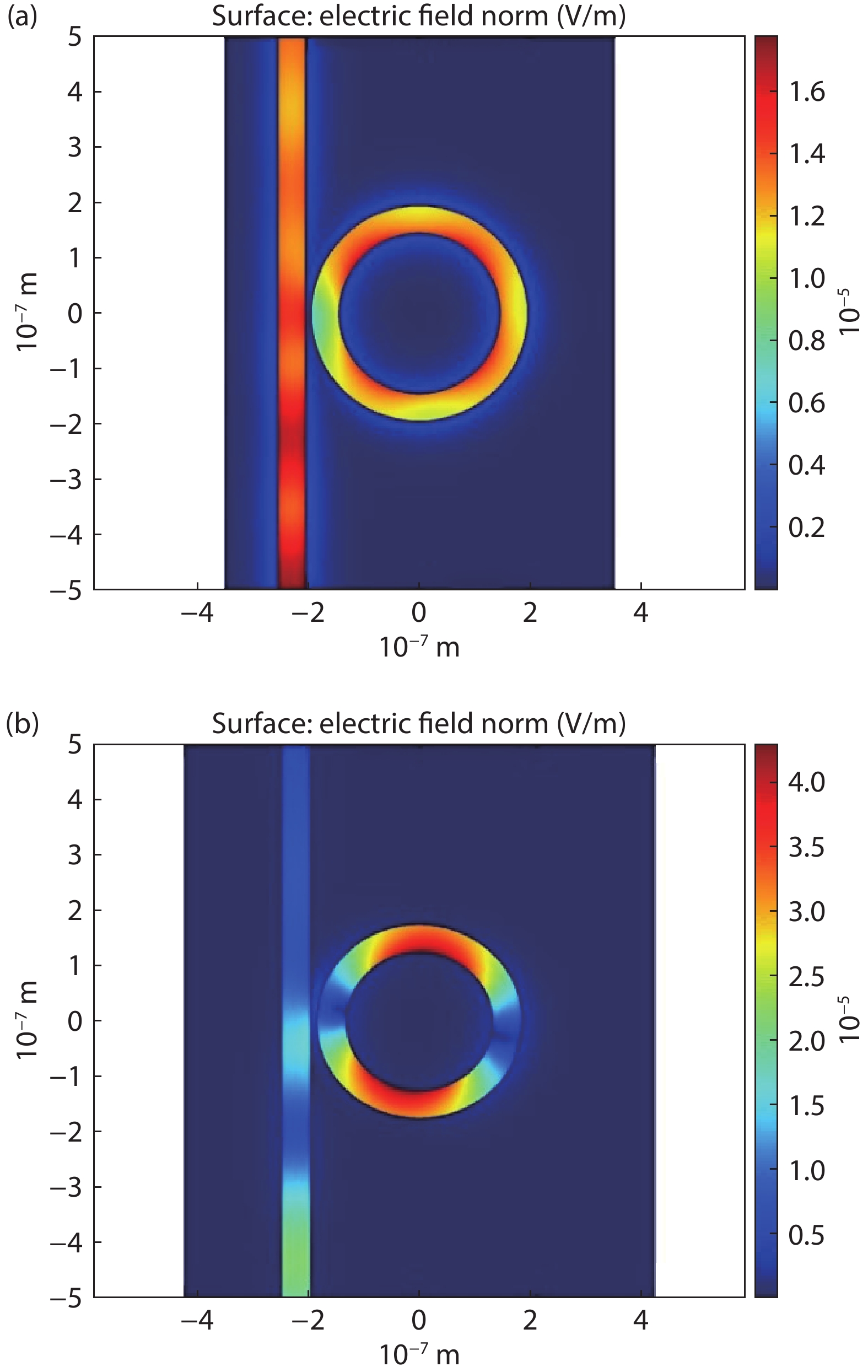
Table 1. Modelling parameters of heavily doped p-silicon by the Lorentz-Drude model.
| Parameter | Value for carrier concentration of 6 × 1019 cm–3 | Value for carrier concentration of 1 × 1020 cm–3 |
| 11.7 | 11.7 | |
| 1.60217662 × 10⁻¹⁹ | 1.60217662 × 10⁻¹⁹ | |
| 50 | 50 | |
| 3.5526595884 × 10⁻³¹ | 3.5526595884 × 10⁻³¹ | |
| 1.2417416061807 × 10⁻¹⁰ | 1.241741606180 × 10⁻¹⁰ | |
| 5.3833134432 × 10⁸ | 8.972189072 × 10⁸ |
 DownLoad: CSV
Table 2. Comparison of relative permittivity of p-silicon between the theoretical value and the experimental value for a carrier concentration of 6 × 1019 cm–3.
| Energy (eV) | Wavelength (μm) | Values of relative permittivity (real part) | Percentage of error (%) | |
| Experimental (Shahzad et al.[9]) | Theoretical (Lorentz-Drude model) | |||
| 0.14 | 8.1 | 4.43 | 2.64 | 40 |
| 0.15 | 7.49 | 4.95 | 3.97 | 19.88 |
| 0.16 | 6.96 | 5.53 | 5.02 | 9.27 |
| 0.17 | 6.5 | 6.12 | 5.87 | 3.95 |
| 0.28 | 4.08 | 9.67 | 9.4 | 2.84 |
| 0.35 | 3.27 | 10.41 | 10.22 | 1.83 |
| 0.42 | 2.73 | 10.82 | 10.67 | 1.45 |
| 0.45 | 2.52 | 10.71 | 10.82 | 1.02 |
DownLoad: CSV
Table 3. Comparison of relative permittivity of p-silicon between the theoretical value and the experimental value for a carrier concentration of 1 × 1020 cm–3.
| Energy (eV) | Wavelength (μm) | Values of relative permittivity (real part) | Percentage of error (%) | |
| Experimental (Shahzad et al.[9]) | Theoretical (Lorentz-Drude model) | |||
| 0.064 | 17.69 | –44.85 | –60.24 | 34.33 |
| 0.067 | 16.72 | –39.97 | –52.62 | 31.66 |
| 0.11 | 10.23 | –17.14 | –12.40 | 27.60 |
| 0.29 | 3.86 | 6.88 | 8.29 | 20.35 |
| 0.30 | 3.71 | 7.56 | 8.53 | 12.86 |
| 0.34 | 3.34 | 8.53 | 9.14 | 7.12 |
| 0.43 | 2.63 | 10.81 | 10.11 | 6.43 |
| 0.46 | 2.49 | 10.81 | 10.27 | 4.98 |
DownLoad: CSV
Table 4. Modelling parameters of gold and silver by the Drude and Lorentz-Drude model.
| Parameter | Value for silver (eV) | Value for gold (eV) |
| Plasma frequency ( | 9.01 | 9.03 |
| Damping constant ( | 0.048 | 0.053 |
| Oscillator strength ( | 0.845 | 0.760 |
| Dominant frequency( | [0.065; 0.011; 0.840; 5.646] | [0.024; 0.010; 0.071; 0.601; 4.384] |
| Damping frequency ( | [3.886; 0.452; 0.065; 0.916; 2.419] | [0.241; 0.345; 0.870; 2.494; 2.214] |
| Resonance frequency ( | [0.816; 4.481; 8.185; 9.083; 20.29] | [0.415; 0.830; 2.969; 4.304; 13.32] |
| Number of resonance | 6 | 6 |
DownLoad: CSV
| [1] |
Barnes W L, Dereux A, Ebbesen T W. Surface plasmon subwavelength optics. Nature, 2003, 424, 824 doi: 10.1038/nature01937
|
| [2] |
Lu H, Liu X, Wang G, et al. Tunable high-channel-count bandpass plasmonic filters based on an analogue of electromagnetically induced transparency. Nanotechnology, 2012, 23, 444003 doi: 10.1088/0957-4484/23/44/444003
|
| [3] |
Wang H Q, Yang J B, Zhang J J, et al. Tunable band-stop plasmonic waveguide filter with symmetrical multiple-teeth-shaped structure. Opt Lett, 2016, 41, 1233 doi: 10.1364/OL.41.001233
|
| [4] |
Johnson P B, Christy R W. Optical constants of the noble metals. Phys Rev B, 1972, 6, 4370 doi: 10.1103/PhysRevB.6.4370
|
| [5] |
West P R, Ishii S, Naik G V, et al. Searching for better plasmonic materials. Laser Photonics Rev, 2010, 4, 795 doi: 10.1002/lpor.200900055
|
| [6] |
Cai W S, Chettiar U K, Kildishev A V, et al. Optical cloaking with metamaterials. Nat Photonics, 2007, 1, 224 doi: 10.1038/nphoton.2007.28
|
| [7] |
Abelès F, Borensztein Y, López Rios T. Optical properties of discontinuous thin films and rough surfaces of silver. In: Advances in Solid State Physics. Berlin, Heidelberg: Springer Berlin Heidelberg, 2007, 93
|
| [8] |
Berestetskii V B, Lifshitz E M, Pitaevskii L P. Quantum Electrodynamics. Volume 4. Butterworth-Heinemann, 1982
|
| [9] |
Shahzad M, Medhi G, Peale R E, et al. Infrared surface plasmons on heavily doped silicon. J Appl Phys, 2011, 110, 123105 doi: 10.1063/1.3672738
|
| [10] |
Linaschke D, Schilling N, Dani I, et al. Highly n-doped surfaces on n-type silicon wafers by laser-chemical processes. Energy Procedia, 2014, 55, 247 doi: 10.1016/j.egypro.2014.08.076
|
| [11] |
Mizushima I, Murakoshi A, Watanabe M, et al. Hole generation without annealing in high dose boron implanted silicon: Heavy doping by B12 icosahedron as a double acceptor. Jpn J Appl Phys, 1994, 33, 404 doi: 10.1143/JJAP.33.404
|
| [12] |
Vi?a L, Cardona M. Effect of heavy doping on the optical properties and the band structure of silicon. Phys Rev B, 1984, 29, 6739 doi: 10.1103/PhysRevB.29.6739
|
| [13] |
Ma Z, Liu Y, Deng L, et al. Heavily boron-doped silicon layer for the fabrication of nanoscale thermoelectric devices. Nanomaterials, 2018, 8, 77 doi: 10.3390/nano8020077
|
| [14] |
Miyao M, Motooka T, Natsuaki N, et al. Change of the electron effective mass in extremely heavily doped n-type Si obtained by ion implantation and laser annealing. Solid State Commun, 1981, 37, 605 doi: 10.1016/0038-1098(81)90144-7
|
| [15] |
Jellison G E, Modine F A, White C W, et al. Optical properties of heavily doped silicon between 1.5 and 4.1 eV. Phys Rev Lett, 1981, 46, 1414 doi: 10.1103/PhysRevLett.46.1414
|
| [16] |
Nobili, Solmi, Parisini, et al. Precipitation, aggregation, and diffusion in heavily arsenic-doped silicon. Phys Rev B, 1994, 49, 2477 doi: 10.1103/PhysRevB.49.2477
|
| [17] |
Maier S A. Spectroscopy and sensing. In: Plasmonics: Fundamentals and Applications. New York, NY: Springer US, 2007, 177
|
| [18] |
Saber M G, Abadía N, Plant D V. CMOS compatible all-silicon TM pass polarizer based on highly doped silicon waveguide. Opt Express, 2018, 26, 20878 doi: 10.1364/OE.26.020878
|
| [19] |
Qi Z P, Hu G H, Li L, et al. Design and analysis of a compact SOI-based aluminum/highly doped p-type silicon hybrid plasmonic modulator. IEEE Photonics J, 2016, 8, 1 doi: 10.1109/JPHOT.2016.2559439
|
| [20] |
Naik G V, Shalaev V M, Boltasseva A. Alternative plasmonic materials: Beyond gold and silver. Adv Mater, 2013, 25, 3264 doi: 10.1002/adma.201205076
|
| [21] |
Chen Y B, Zhang Z M. Heavily doped silicon complex gratings as wavelength-selective absorbing surfaces. J Phys D, 2008, 41, 095406 doi: 10.1088/0022-3727/41/9/095406
|
| [22] |
Schroder D K, Thomas R N, Swartz J C. Free carrier absorption in silicon. IEEE J Solid-State Circuits, 1978, 13, 180 doi: 10.1109/JSSC.1978.1051012
|
| [23] |
van Exter M, Grischkowsky D. Carrier dynamics of electrons and holes in moderately doped silicon. Phys Rev B, 1990, 41, 12140 doi: 10.1103/PhysRevB.41.12140
|
| [24] |
Raki? A D, Djuri?i? A B, Elazar J M, et al. Optical properties of metallic films for vertical-cavity optoelectronic devices. Appl Opt, 1998, 37, 5271 doi: 10.1364/AO.37.005271
|
| [25] |
Kildishev A V, Shalaev V M. Engineering space for light via transformation optics. Opt Lett, 2008, 33, 43 doi: 10.1364/OL.33.000043
|
| [26] |
Cai W S, Chettiar U K, Kildishev A V, et al. Designs for optical cloaking with high-order transformations. Opt Express, 2008, 16, 5444 doi: 10.1364/OE.16.005444
|


Article views: 4960 Times PDF downloads: 118 Times Cited by: 0 Times
Received: 26 September 2020 Revised: 05 January 2021 Online: Accepted Manuscript: 15 March 2021Uncorrected proof: 23 March 2021Published: 01 June 2021
| Citation: |
Md. Omar Faruque, Rabiul Al Mahmud, Rakibul Hasan Sagor. Heavily doped silicon: A potential replacement of conventional plasmonic metals[J]. Journal of Semiconductors, 2021, 42(6): 062302. doi: 10.1088/1674-4926/42/6/062302
****
M O Faruque, R Al Mahmud, R H Sagor, Heavily doped silicon: A potential replacement of conventional plasmonic metals[J]. J. Semicond., 2021, 42(6): 062302. doi: 10.1088/1674-4926/42/6/062302.

|
| [1] |
Barnes W L, Dereux A, Ebbesen T W. Surface plasmon subwavelength optics. Nature, 2003, 424, 824 doi: 10.1038/nature01937
|
| [2] |
Lu H, Liu X, Wang G, et al. Tunable high-channel-count bandpass plasmonic filters based on an analogue of electromagnetically induced transparency. Nanotechnology, 2012, 23, 444003 doi: 10.1088/0957-4484/23/44/444003
|
| [3] |
Wang H Q, Yang J B, Zhang J J, et al. Tunable band-stop plasmonic waveguide filter with symmetrical multiple-teeth-shaped structure. Opt Lett, 2016, 41, 1233 doi: 10.1364/OL.41.001233
|
| [4] |
Johnson P B, Christy R W. Optical constants of the noble metals. Phys Rev B, 1972, 6, 4370 doi: 10.1103/PhysRevB.6.4370
|
| [5] |
West P R, Ishii S, Naik G V, et al. Searching for better plasmonic materials. Laser Photonics Rev, 2010, 4, 795 doi: 10.1002/lpor.200900055
|
| [6] |
Cai W S, Chettiar U K, Kildishev A V, et al. Optical cloaking with metamaterials. Nat Photonics, 2007, 1, 224 doi: 10.1038/nphoton.2007.28
|
| [7] |
Abelès F, Borensztein Y, López Rios T. Optical properties of discontinuous thin films and rough surfaces of silver. In: Advances in Solid State Physics. Berlin, Heidelberg: Springer Berlin Heidelberg, 2007, 93
|
| [8] |
Berestetskii V B, Lifshitz E M, Pitaevskii L P. Quantum Electrodynamics. Volume 4. Butterworth-Heinemann, 1982
|
| [9] |
Shahzad M, Medhi G, Peale R E, et al. Infrared surface plasmons on heavily doped silicon. J Appl Phys, 2011, 110, 123105 doi: 10.1063/1.3672738
|
| [10] |
Linaschke D, Schilling N, Dani I, et al. Highly n-doped surfaces on n-type silicon wafers by laser-chemical processes. Energy Procedia, 2014, 55, 247 doi: 10.1016/j.egypro.2014.08.076
|
| [11] |
Mizushima I, Murakoshi A, Watanabe M, et al. Hole generation without annealing in high dose boron implanted silicon: Heavy doping by B12 icosahedron as a double acceptor. Jpn J Appl Phys, 1994, 33, 404 doi: 10.1143/JJAP.33.404
|
| [12] |
Vi?a L, Cardona M. Effect of heavy doping on the optical properties and the band structure of silicon. Phys Rev B, 1984, 29, 6739 doi: 10.1103/PhysRevB.29.6739
|
| [13] |
Ma Z, Liu Y, Deng L, et al. Heavily boron-doped silicon layer for the fabrication of nanoscale thermoelectric devices. Nanomaterials, 2018, 8, 77 doi: 10.3390/nano8020077
|
| [14] |
Miyao M, Motooka T, Natsuaki N, et al. Change of the electron effective mass in extremely heavily doped n-type Si obtained by ion implantation and laser annealing. Solid State Commun, 1981, 37, 605 doi: 10.1016/0038-1098(81)90144-7
|
| [15] |
Jellison G E, Modine F A, White C W, et al. Optical properties of heavily doped silicon between 1.5 and 4.1 eV. Phys Rev Lett, 1981, 46, 1414 doi: 10.1103/PhysRevLett.46.1414
|
| [16] |
Nobili, Solmi, Parisini, et al. Precipitation, aggregation, and diffusion in heavily arsenic-doped silicon. Phys Rev B, 1994, 49, 2477 doi: 10.1103/PhysRevB.49.2477
|
| [17] |
Maier S A. Spectroscopy and sensing. In: Plasmonics: Fundamentals and Applications. New York, NY: Springer US, 2007, 177
|
| [18] |
Saber M G, Abadía N, Plant D V. CMOS compatible all-silicon TM pass polarizer based on highly doped silicon waveguide. Opt Express, 2018, 26, 20878 doi: 10.1364/OE.26.020878
|
| [19] |
Qi Z P, Hu G H, Li L, et al. Design and analysis of a compact SOI-based aluminum/highly doped p-type silicon hybrid plasmonic modulator. IEEE Photonics J, 2016, 8, 1 doi: 10.1109/JPHOT.2016.2559439
|
| [20] |
Naik G V, Shalaev V M, Boltasseva A. Alternative plasmonic materials: Beyond gold and silver. Adv Mater, 2013, 25, 3264 doi: 10.1002/adma.201205076
|
| [21] |
Chen Y B, Zhang Z M. Heavily doped silicon complex gratings as wavelength-selective absorbing surfaces. J Phys D, 2008, 41, 095406 doi: 10.1088/0022-3727/41/9/095406
|
| [22] |
Schroder D K, Thomas R N, Swartz J C. Free carrier absorption in silicon. IEEE J Solid-State Circuits, 1978, 13, 180 doi: 10.1109/JSSC.1978.1051012
|
| [23] |
van Exter M, Grischkowsky D. Carrier dynamics of electrons and holes in moderately doped silicon. Phys Rev B, 1990, 41, 12140 doi: 10.1103/PhysRevB.41.12140
|
| [24] |
Raki? A D, Djuri?i? A B, Elazar J M, et al. Optical properties of metallic films for vertical-cavity optoelectronic devices. Appl Opt, 1998, 37, 5271 doi: 10.1364/AO.37.005271
|
| [25] |
Kildishev A V, Shalaev V M. Engineering space for light via transformation optics. Opt Lett, 2008, 33, 43 doi: 10.1364/OL.33.000043
|
| [26] |
Cai W S, Chettiar U K, Kildishev A V, et al. Designs for optical cloaking with high-order transformations. Opt Express, 2008, 16, 5444 doi: 10.1364/OE.16.005444
|

 WeChat ID
Journal of Semiconductors © 2017 All Rights Reserved 京ICP備05085259號(hào)-2

