


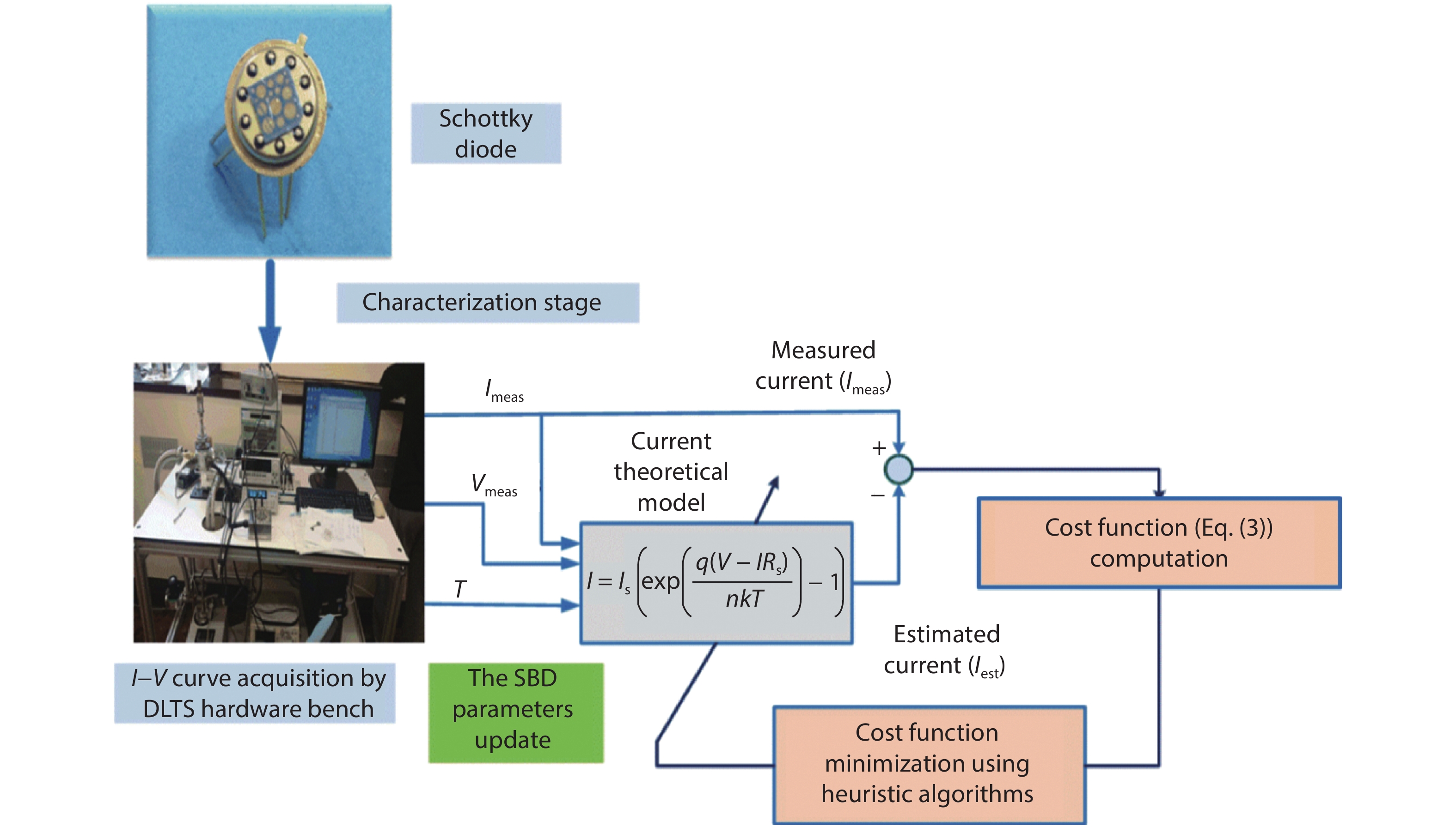
Fig. 1.
(Color online) The Schottky diode parameters extraction strategy.
ARTICLES
Elyes Garoudja1, , Walid Filali1, Slimane Oussalah2, Noureddine Sengouga3 and Mohamed Henini4
Corresponding author: Elyes Garoudja, egaroudja@cdta.dz
Abstract: In this work, forward current voltage characteristics for multi-quantum wells Al0.33Ga0.67As Schottky diode were measured at temperature ranges from 100 to 300 K. The main parameters of this Schottky diode, such as the ideality factor, barrier height, series resistance and saturation current, have been extracted using both analytical and heuristics methods. Differential evolution (DE), particle swarm optimization (PSO) and artificial bee colony (ABC) have been chosen as candidate heuristics algorithms, while Cheung technic was selected as analytical extraction method. The obtained results show clearly the high performance of DE algorithms in terms of parameters accuracy, convergence speed and robustness.
Key words: barrier height, heuristic methods, multi-quantum wells, parameters extraction, Schottky diode
| [1] |
Cheung S, Cheung N. Extraction of Schottky diode parameters from forward current–voltage characteristics. Appl Phys Lett, 1986, 49(2), 85 doi: 10.1063/1.97359
|
| [2] |
Werner J H. Schottky barrier and pn-junction I/V plots—Small signal evaluation. Appl Phys A, 1988, 47(3), 291 doi: 10.1007/BF00615935
|
| [3] |
Karata? ?, Alt?ndal ?. Temperature dependence of barrier heights of Au/n-type GaAs Schottky diodes. Solid-State Electron, 2005, 49(6), 1052 doi: 10.1016/j.sse.2005.02.005
|
| [4] |
D?kme ?, Altindal ?, Bülbül M M. The barrier height inhomogeneity in Al/p-Si Schottky barrier diodes with native insulator layer. Appl Surf Sci, 2006, 252(22), 7749 doi: 10.1016/j.apsusc.2005.09.046
|
| [5] |
Karaboga N, Kockanat S, Dogan H. Parameter determination of the schottky barrier diode using by artificial bee colony algorithm. International Symposium on Innovations in Intelligent Systems and Applications, 2011, 6
|
| [6] |
Sellai A, Ouennoughi Z. Extraction of illuminated solar cell and Schottky diode parameters using a genetic algorithm. Int J Mod Phys C, 2005, 16(07), 1043 doi: 10.1142/S0129183105007704
|
| [7] |
Werner J H, Güttler H H. Barrier inhomogeneities at Schottky contacts. J Appl Phys, 1991, 69(3), 1522 doi: 10.1063/1.347243
|
| [8] |
Norde H. A modified forward I–V plot for Schottky diodes with high series resistance. J Appl Phys, 1979, 50(7), 5052 doi: 10.1063/1.325607
|
| [9] |
Garoudja E, Kara K, Chouder A, et al. Parameters extraction of photovoltaic module for long-term prediction using artifical bee colony optimization. 3rd International Conference on Control, Engineering & Information Technology (CEIT), 2015, 1
|
| [10] |
Li F, Mudanai S P, Fan Y Y, et al. A simulated annealing approach for automatic extraction of device and material parameters of MOS with SiO2 high-K gate stacks. Proceedings of the 15th Biennial University/Government/Industry Microelectronics Symposium (Cat. No. 03CH37488), 2003, 218
|
| [11] |
Wang K, Ye M. Parameter determination of Schottky-barrier diode model using differential evolution. Solid-State Electron, 2009, 53(2), 234 doi: 10.1016/j.sse.2008.11.010
|
| [12] |
Kennedy J. Particle swarm optimization. Encyclopedia of Machine Learning, 2010, 760
|
| [13] |
Schroder D K. Semiconductor material and device characterization. John Wiley & Sons, 2006
|
| [14] |
Mathieu H, Fanet H. Physique des semiconducteurs et des composants électroniques. Dunod Paris, 2001 (in French)
|
| [15] |
Sze S M, Ng K K. Physics of semiconductor devices. John Wiley & Sons, 2006
|
| [16] |
Filali W, Sengouga N, Oussalah S, et al. Characterisation of temperature dependent parameters of multi-quantum well (MQW) Ti/Au/n-AlGaAs/n-GaAs/n-AlGaAs Schottky diodes. Superlattices Microstruct, 2017, 111, 1010 doi: 10.1016/j.spmi.2017.07.059
|
| [17] |
Mari R. Electrical characterization of defects in III–V compound semiconductors by DLTS. PhD Thesis, University of Nottingham, 2011
|
| [18] |
Filali W, Oussalah S, Sengouga N, et al. Simulation of p-type Schottky diode based on Al0.29Ga0.71As with titanium/gold Schottky contact. 30th International Conference on Microelectronics (ICM), 2019, 272
|
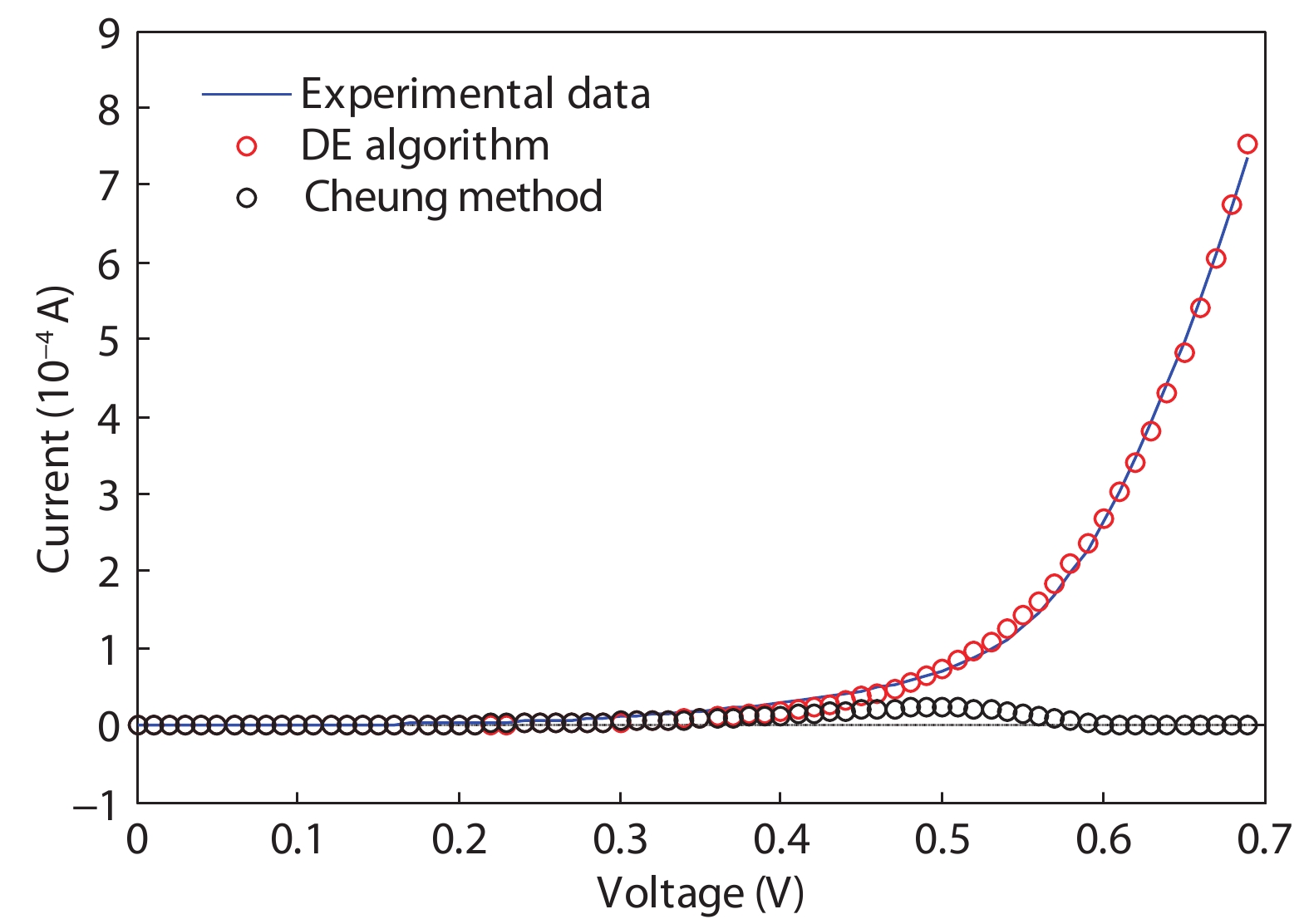
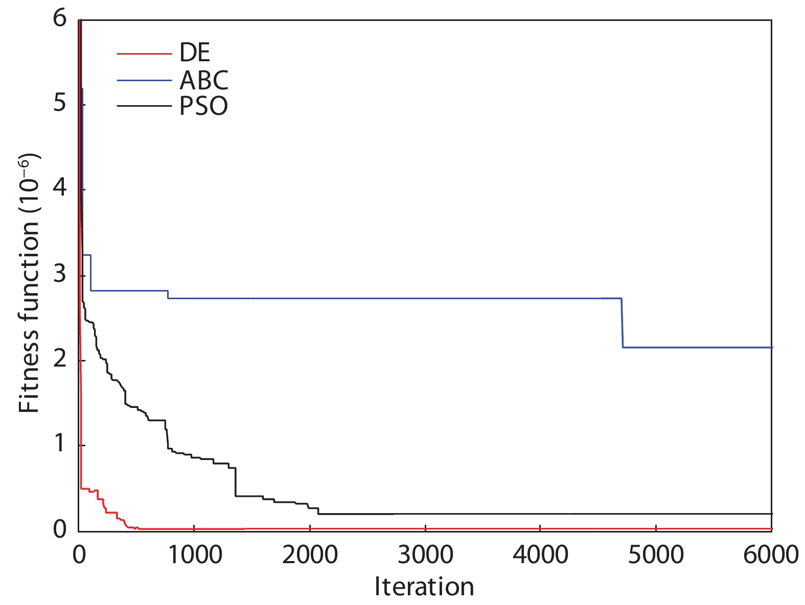
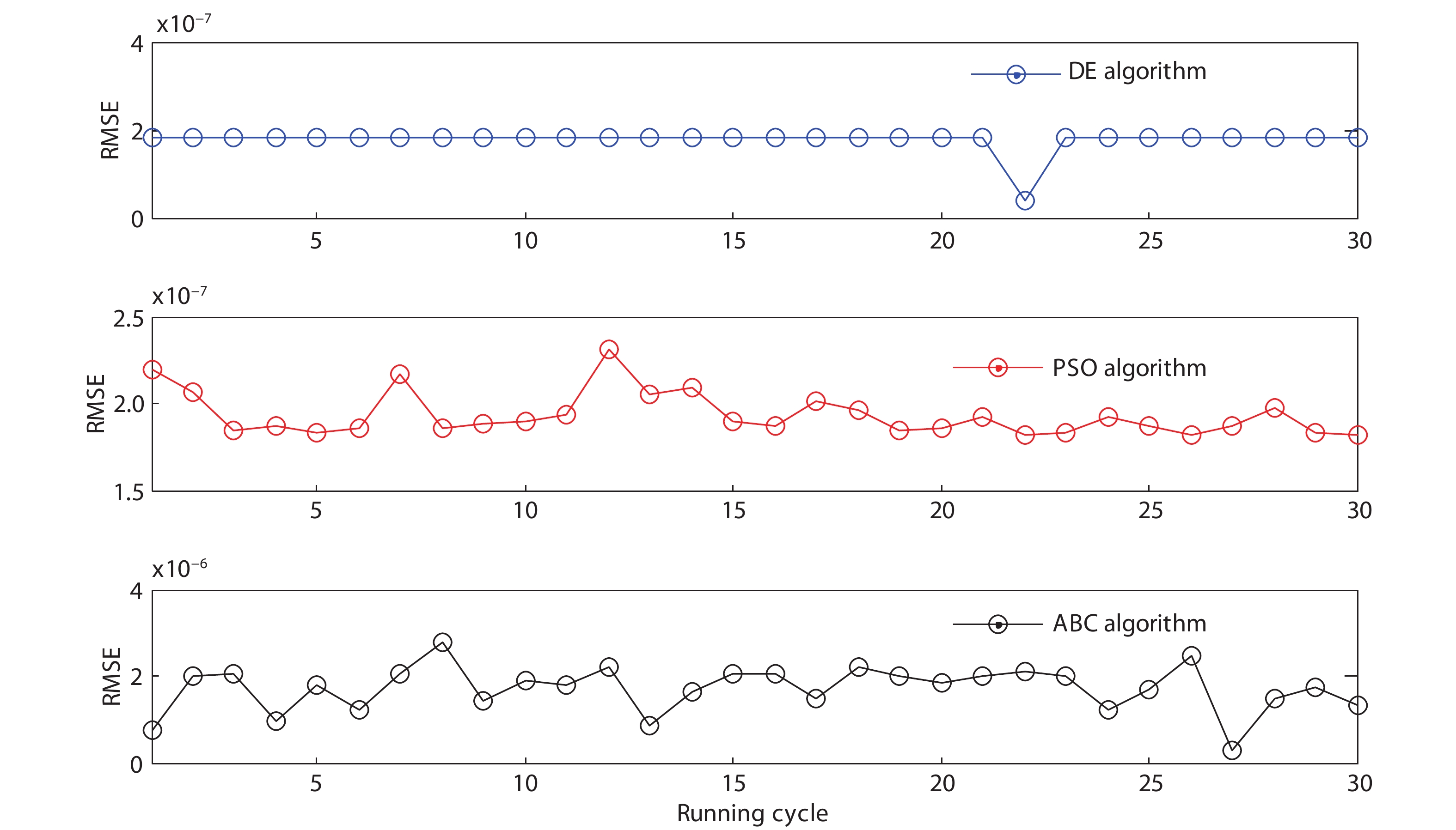
Table 1. The setting parameters of DE, PSO and ABC algorithms.
| DE | PSO | ABC |
| Population size: 40 CR: 0.2 MF: 0.5 | Swarm size: 100 Inertia weight: 0.4–0.7 C1, C2: 1.2,1.6 | Colony size: 160 Limit: 3 × 160 = 480 Cycle: 5000 |
 DownLoad: CSV
Table 2. The variation range of SBD parameters.
| Parameter | Is (A) | n | Rs (?) |
| Variation boundary | [10–9, 10–6] | [0, 20] | [0, 104] |
DownLoad: CSV
Table 3. The obtained results for the temperature range (100–160 K).
| Temparature | Parameter | DE | PSO | ABC | Cheung |
| T = 100 K | Is | 1.069 × 10⁻⁷ | 1.352 × 10⁻⁷ | 4.816 × 10⁻⁷ | 5.00 × 10⁻⁸ |
| n | 9.602 | 10.076 | 13.28 | 8.61 | |
| Rs | 1.717 × 10³ | 1.633 × 10³ | 1.286 × 10³ | 2217.09 | |
| фb | 0.176 | 0.174 | 0.163 | 0.20 | |
| RMSE | 1.816 × 10⁻⁷ | 2.715 × 10⁻⁷ | 2.131 × 10⁻⁶ | 1.064 × 10⁻⁵ | |
| Mean | 1.816 × 10⁻⁷ | 1.086 × 10⁻⁷ | 2.693 × 10⁻⁶ | – | |
| STD | 8.050 × 10⁻²² | 1.487 × 10⁻⁷ | 4.180 × 10⁻⁷ | – | |
| T = 120 K | Is | 1.105 × 10⁻⁷ | 1.083 × 10⁻⁷ | 1.784 × 10⁻⁷ | 5.00 × 10⁻⁸ |
| n | 7.907 | 7.875 | 8.664 | 7.12 | |
| Rs | 1.630 × 10³ | 1.637 × 10³ | 1.520 × 10³ | 2.114 × 10³ | |
| фb | 0.214 | 0.215 | 0.20 | 0.24 | |
| RMSE | 1.679 × 10⁻⁷ | 1.690 × 10⁻⁷ | 1.498 × 10⁻⁶ | 1.305 × 10⁻⁵ | |
| Mean | 1.679 × 10⁻⁷ | 6.763 × 10⁻⁸ | 2.635 × 10⁻⁶ | – | |
| STD | 2.813 × 10⁻²² | 9.261 × 10⁻⁸ | 4.234 × 10⁻⁷ | – | |
| T = 160 K | Is | 1.437 × 10⁻⁷ | 1.402 × 10⁻⁷ | 9.953 × 10⁻⁷ | 6.00 × 10⁻⁸ |
| n | 5.962 | 5.937 | 9.935 | 5.27 | |
| Rs | 1.483 × 10³ | 1.482 × 10³ | 4.58 × 10² | 1.875 × 10³ | |
| фb | 0.290 | 0.291 | 0.26 | 0.33 | |
| RMSE | 4.011 × 10⁻⁷ | 4.116 × 10⁻⁷ | 2.601 × 10⁻⁶ | 1.394 × 10⁻⁵ | |
| Mean | 4.011 × 10⁻⁷ | 1.646 × 10⁻⁷ | 2.831 × 10⁻⁶ | – | |
| STD | 1.123 × 10⁻²¹ | 2.254 × 10⁻⁷ | 4.306 × 10⁻⁷ | – |
DownLoad: CSV
Table 4. The obtained results for the temperature range (200–300 K).
| Temparature | Parameter | DE | PSO | ABC | Cheung |
| T = 200 K | Is | 2.347 × 10⁻⁷ | 2.304 × 10⁻⁷ | 5.560 × 10⁻⁷ | 7.00 × 10⁻⁸ |
| n | 5.064 | 5.051 | 6.204 | 4.19 | |
| Rs | 1.282 × 10³ | 1.280 × 10³ | 1.017 × 10³ | 1.758 × 10³ | |
| фb | 0.362 | 0.363 | 0.347 | 0.42 | |
| RMSE | 7.96 × 10⁻⁷ | 8.005 × 10⁻⁷ | 1.441 × 10⁻⁶ | 1.829 × 10⁻⁵ | |
| Mean | 7.968 × 10⁻⁷ | 3.202 × 10⁻⁷ | 2.970 × 10⁻⁶ | – | |
| STD | 5.989 × 10⁻²² | 4.384 × 10⁻⁷ | 8.012 × 10⁻⁷ | – | |
| T = 220 K | Is | 9.245 × 10⁻⁷ | 9.165 × 10⁻⁷ | 1 × 10⁻⁶ | 8.00 × 10⁻⁸ |
| n | 6.623 | 6.604 | 6.799 | 3.79 | |
| Rs | 4.871 × 10² | 4.92 × 10² | 4.405 × 10² | 1.736 × 10³ | |
| фb | 0.376 | 0.376 | 0.375 | 0.46 | |
| RMSE | 2.119 × 10⁻⁶ | 2.149 × 10⁻⁶ | 2.211 × 10⁻⁶ | 2.315 × 10⁻⁵ | |
| Mean | 2.119 × 10⁻⁶ | 8.596 × 10⁻⁷ | 3.134 × 10⁻⁶ | – | |
| STD | 9.470 × 10⁻²² | 1.177 × 10⁻⁶ | 2.519 × 10⁻⁷ | – | |
| T = 240 K | Is | 1.212 × 10⁻⁷ | 1.364 × 10⁻⁷ | 8.229 × 10⁻⁷ | 1.00 × 10⁻⁷ |
| n | 3.372 | 3.486 | 6.078 | 3.46 | |
| Rs | 1.799 × 10³ | 1.622 × 10³ | 100.23 | 1.693 × 10³ | |
| фb | 0.456 | 0.454 | 0.416 | 0.51 | |
| RMSE | 1.768 × 10⁻⁸ | 5.763 × 10⁻⁸ | 4.810 × 10⁻⁶ | 4.147 × 10⁻⁵ | |
| Mean | 1.768 × 10⁻⁸ | 2.307 × 10⁻⁸ | 6.223 × 10⁻⁶ | – | |
| STD | 1.544 × 10⁻²² | 3.159 × 10⁻⁸ | 6.973 × 10⁻⁷ | – | |
| T = 300 K | Is | 2.063 × 10⁻⁷ | 4.208 × 10⁻⁷ | 8.450 × 10⁻⁸ | 1.00 × 10⁻⁷ |
| n | 2.762 | 3.468 | 2.874 | 2.82 | |
| Rs | 1.560 × 10³ | 6.496 × 10² | 17.676 | 1.480 × 10³ | |
| фb | 0.568 | 0.549 | 0.591 | 0.63 | |
| RMSE | 2.539 × 10⁻⁸ | 3.959 × 10⁻⁷ | 9.856 × 10⁻⁶ | 1.971 × 10⁻⁴ | |
| Mean | 2.539 × 10⁻⁸ | 1.583 × 10⁻⁷ | 1.329 × 10⁻⁵ | – | |
| STD | 3.766 × 10⁻²² | 2.168 × 10⁻⁷ | 1.170 × 10⁻⁵ | – |
DownLoad: CSV
| [1] |
Cheung S, Cheung N. Extraction of Schottky diode parameters from forward current–voltage characteristics. Appl Phys Lett, 1986, 49(2), 85 doi: 10.1063/1.97359
|
| [2] |
Werner J H. Schottky barrier and pn-junction I/V plots—Small signal evaluation. Appl Phys A, 1988, 47(3), 291 doi: 10.1007/BF00615935
|
| [3] |
Karata? ?, Alt?ndal ?. Temperature dependence of barrier heights of Au/n-type GaAs Schottky diodes. Solid-State Electron, 2005, 49(6), 1052 doi: 10.1016/j.sse.2005.02.005
|
| [4] |
D?kme ?, Altindal ?, Bülbül M M. The barrier height inhomogeneity in Al/p-Si Schottky barrier diodes with native insulator layer. Appl Surf Sci, 2006, 252(22), 7749 doi: 10.1016/j.apsusc.2005.09.046
|
| [5] |
Karaboga N, Kockanat S, Dogan H. Parameter determination of the schottky barrier diode using by artificial bee colony algorithm. International Symposium on Innovations in Intelligent Systems and Applications, 2011, 6
|
| [6] |
Sellai A, Ouennoughi Z. Extraction of illuminated solar cell and Schottky diode parameters using a genetic algorithm. Int J Mod Phys C, 2005, 16(07), 1043 doi: 10.1142/S0129183105007704
|
| [7] |
Werner J H, Güttler H H. Barrier inhomogeneities at Schottky contacts. J Appl Phys, 1991, 69(3), 1522 doi: 10.1063/1.347243
|
| [8] |
Norde H. A modified forward I–V plot for Schottky diodes with high series resistance. J Appl Phys, 1979, 50(7), 5052 doi: 10.1063/1.325607
|
| [9] |
Garoudja E, Kara K, Chouder A, et al. Parameters extraction of photovoltaic module for long-term prediction using artifical bee colony optimization. 3rd International Conference on Control, Engineering & Information Technology (CEIT), 2015, 1
|
| [10] |
Li F, Mudanai S P, Fan Y Y, et al. A simulated annealing approach for automatic extraction of device and material parameters of MOS with SiO2 high-K gate stacks. Proceedings of the 15th Biennial University/Government/Industry Microelectronics Symposium (Cat. No. 03CH37488), 2003, 218
|
| [11] |
Wang K, Ye M. Parameter determination of Schottky-barrier diode model using differential evolution. Solid-State Electron, 2009, 53(2), 234 doi: 10.1016/j.sse.2008.11.010
|
| [12] |
Kennedy J. Particle swarm optimization. Encyclopedia of Machine Learning, 2010, 760
|
| [13] |
Schroder D K. Semiconductor material and device characterization. John Wiley & Sons, 2006
|
| [14] |
Mathieu H, Fanet H. Physique des semiconducteurs et des composants électroniques. Dunod Paris, 2001 (in French)
|
| [15] |
Sze S M, Ng K K. Physics of semiconductor devices. John Wiley & Sons, 2006
|
| [16] |
Filali W, Sengouga N, Oussalah S, et al. Characterisation of temperature dependent parameters of multi-quantum well (MQW) Ti/Au/n-AlGaAs/n-GaAs/n-AlGaAs Schottky diodes. Superlattices Microstruct, 2017, 111, 1010 doi: 10.1016/j.spmi.2017.07.059
|
| [17] |
Mari R. Electrical characterization of defects in III–V compound semiconductors by DLTS. PhD Thesis, University of Nottingham, 2011
|
| [18] |
Filali W, Oussalah S, Sengouga N, et al. Simulation of p-type Schottky diode based on Al0.29Ga0.71As with titanium/gold Schottky contact. 30th International Conference on Microelectronics (ICM), 2019, 272
|


Article views: 4921 Times PDF downloads: 88 Times Cited by: 0 Times
Received: 28 November 2019 Revised: 04 February 2020 Online: Accepted Manuscript: 07 April 2020Uncorrected proof: 24 April 2020Published: 01 October 2020
| Citation: |
Elyes Garoudja, Walid Filali, Slimane Oussalah, Noureddine Sengouga, Mohamed Henini. Comparative study of various methods for extraction of multi- quantum wells Schottky diode parameters[J]. Journal of Semiconductors, 2020, 41(10): 102401. doi: 10.1088/1674-4926/41/10/102401
****
E Garoudja, W Filali, S Oussalah, N Sengouga, M Henini, Comparative study of various methods for extraction of multi- quantum wells Schottky diode parameters[J]. J. Semicond., 2020, 41(10): 102401. doi: 10.1088/1674-4926/41/10/102401.

|
| [1] |
Cheung S, Cheung N. Extraction of Schottky diode parameters from forward current–voltage characteristics. Appl Phys Lett, 1986, 49(2), 85 doi: 10.1063/1.97359
|
| [2] |
Werner J H. Schottky barrier and pn-junction I/V plots—Small signal evaluation. Appl Phys A, 1988, 47(3), 291 doi: 10.1007/BF00615935
|
| [3] |
Karata? ?, Alt?ndal ?. Temperature dependence of barrier heights of Au/n-type GaAs Schottky diodes. Solid-State Electron, 2005, 49(6), 1052 doi: 10.1016/j.sse.2005.02.005
|
| [4] |
D?kme ?, Altindal ?, Bülbül M M. The barrier height inhomogeneity in Al/p-Si Schottky barrier diodes with native insulator layer. Appl Surf Sci, 2006, 252(22), 7749 doi: 10.1016/j.apsusc.2005.09.046
|
| [5] |
Karaboga N, Kockanat S, Dogan H. Parameter determination of the schottky barrier diode using by artificial bee colony algorithm. International Symposium on Innovations in Intelligent Systems and Applications, 2011, 6
|
| [6] |
Sellai A, Ouennoughi Z. Extraction of illuminated solar cell and Schottky diode parameters using a genetic algorithm. Int J Mod Phys C, 2005, 16(07), 1043 doi: 10.1142/S0129183105007704
|
| [7] |
Werner J H, Güttler H H. Barrier inhomogeneities at Schottky contacts. J Appl Phys, 1991, 69(3), 1522 doi: 10.1063/1.347243
|
| [8] |
Norde H. A modified forward I–V plot for Schottky diodes with high series resistance. J Appl Phys, 1979, 50(7), 5052 doi: 10.1063/1.325607
|
| [9] |
Garoudja E, Kara K, Chouder A, et al. Parameters extraction of photovoltaic module for long-term prediction using artifical bee colony optimization. 3rd International Conference on Control, Engineering & Information Technology (CEIT), 2015, 1
|
| [10] |
Li F, Mudanai S P, Fan Y Y, et al. A simulated annealing approach for automatic extraction of device and material parameters of MOS with SiO2 high-K gate stacks. Proceedings of the 15th Biennial University/Government/Industry Microelectronics Symposium (Cat. No. 03CH37488), 2003, 218
|
| [11] |
Wang K, Ye M. Parameter determination of Schottky-barrier diode model using differential evolution. Solid-State Electron, 2009, 53(2), 234 doi: 10.1016/j.sse.2008.11.010
|
| [12] |
Kennedy J. Particle swarm optimization. Encyclopedia of Machine Learning, 2010, 760
|
| [13] |
Schroder D K. Semiconductor material and device characterization. John Wiley & Sons, 2006
|
| [14] |
Mathieu H, Fanet H. Physique des semiconducteurs et des composants électroniques. Dunod Paris, 2001 (in French)
|
| [15] |
Sze S M, Ng K K. Physics of semiconductor devices. John Wiley & Sons, 2006
|
| [16] |
Filali W, Sengouga N, Oussalah S, et al. Characterisation of temperature dependent parameters of multi-quantum well (MQW) Ti/Au/n-AlGaAs/n-GaAs/n-AlGaAs Schottky diodes. Superlattices Microstruct, 2017, 111, 1010 doi: 10.1016/j.spmi.2017.07.059
|
| [17] |
Mari R. Electrical characterization of defects in III–V compound semiconductors by DLTS. PhD Thesis, University of Nottingham, 2011
|
| [18] |
Filali W, Oussalah S, Sengouga N, et al. Simulation of p-type Schottky diode based on Al0.29Ga0.71As with titanium/gold Schottky contact. 30th International Conference on Microelectronics (ICM), 2019, 272
|

 WeChat ID
Journal of Semiconductors © 2017 All Rights Reserved 京ICP備05085259號-2

