Fig. 1.
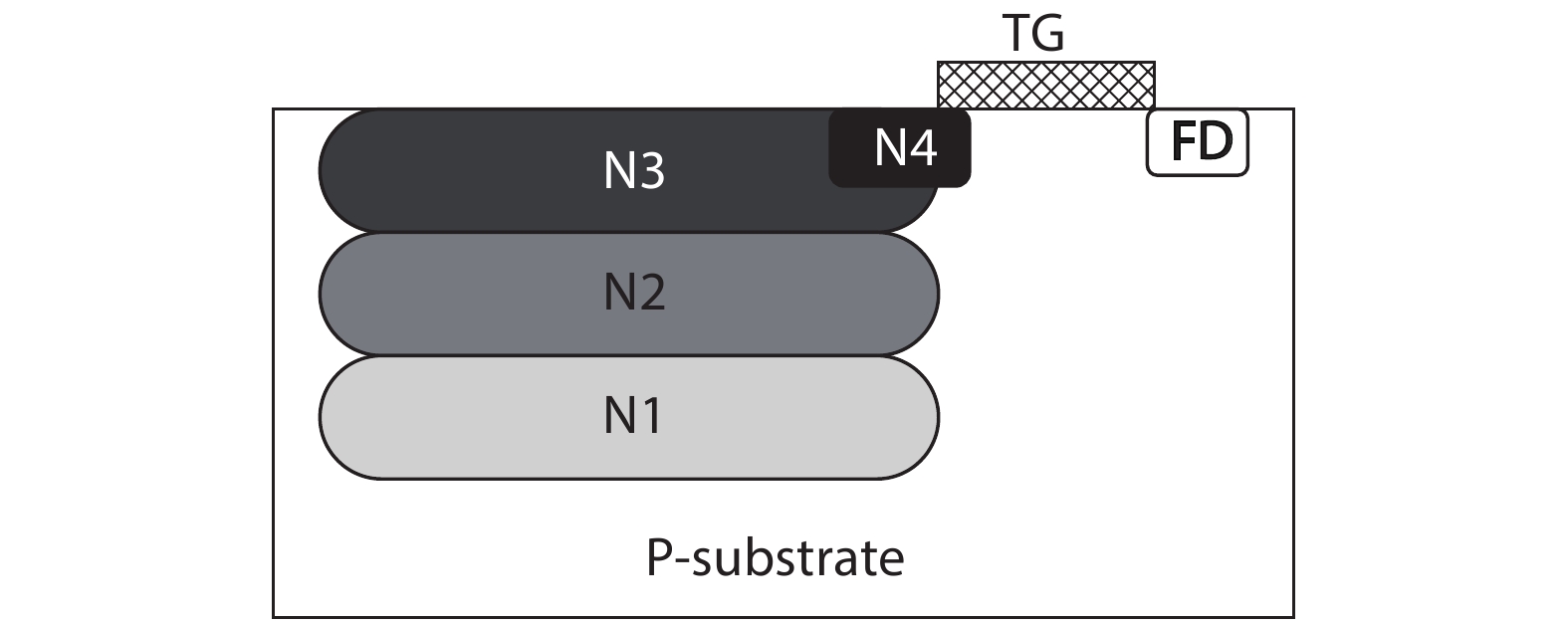
N buried layer structure of PPD.
ARTICLES
Feng Li1, Ruishuo Wang1, Liqiang Han2 and Jiangtao Xu1,
Corresponding author: Jiangtao Xu, Email: xujiangtao@tju.edu.cn
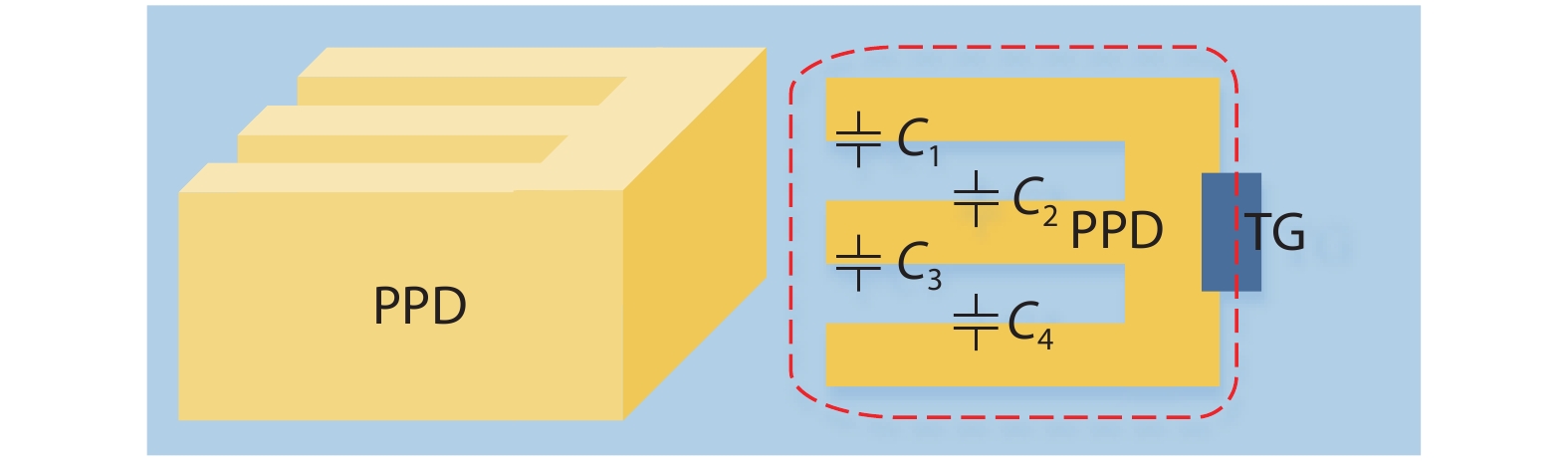
Abstract: To improve the full-well capacity and linear dynamic range of CMOS image sensor, a special finger-shaped pinned photodiode (PPD) is designed. In terms of process, the first N-type ion implantation of the PPD N buried layer is extended under the transfer gate, thereby increasing the PPD capacitance. Based on TCAD simulation, the width and spacing of PPD were precisely adjusted. A high full-well capacity pixel design with a pixel size of 6 × 6 μm2 is realized based on the 0.18 μm CMOS process. The simulation results indicate that the pixel with the above structure and process has a depletion depth of 2.8 μm and a charge transfer efficiency of 100%. The measurement results of the test chip show that the full-well capacity can reach 68650e–. Compared with the conventional structure, the proposed PPD structure can effectively improve the full well capacity of the pixel.
Key words: CMOS active pixel, full well capacity, full depletion
| [1] |
Bigas M, Cabruja E, Forest J, et al. Review of CMOS image sensor. Microelectron J, 2006, 37(5), 433 doi: 10.1016/j.mejo.2005.07.002
|
| [2] |
Luo B, Yang F X, Yan L. Key technologies and research development of CMOS image sensors. IITA International Conference on Geoscience and Remote Sensing, 2010, 322
|
| [3] |
Fontaine R. Innovative technology elements for large and small pixel CIS devices. Proc International Image Sensor Workshop (IISW), 2013, 1
|
| [4] |
Wang X D, Ye T. Comparative research and future tendency between CMOS and CCD image sensor. Electron Des Eng, 2010, 18(11), 184
|
| [5] |
Jan B, Erik J M, Wilco K, et al. Recent developments on large-area CCDs for professional applications. International image sensor workshop. Proc International Image Sensor Workshop (IISW), 2015, 1
|
| [6] |
Velichko S, Hynecek J, Johnson R, et al. CMOS global shutter charge storage pixels with improved performance. IEEE Trans Electron Devices, 2015, 63(1), 1 doi: 10.1109/TED.2015.2443495
|
| [7] |
Solhusvik J, Kuang J, Lin Z, et al. A comparison of high dynamic range CIS technologies for automotive applications. Proc International Image Sensor Workshop, 2013, 1
|
| [8] |
Freedman S D, Boussaid F. A high dynamic range CMOS image sensor with a novel pixel-level logarithmic counter memory. IEEE International Conference on Knowledge-Based Engineering and Innovation (KBEI), 2015, 14
|
| [9] |
Takayanagi I, Yoshimura N, Mori K, et al. An 87 dB single exposure dynamic range CMOS image sensor with a 3.0 μm triple conversion gain pixel. Proc International Image Sensor Workshop (IISW), 2017, 30
|
| [10] |
Wang R G, Yin Y X, Liang L, et al. A high dynamic range CMOS image sensor with dual charge transfer phase. IEEE International Conference on Solid-State and Integrated Circuit Technology (ICSICT), 2016, 1369
|
| [11] |
Yu J T, Li B Q, Yu P P, et al. Two-dimensional pixel image lag simulation and optimization in a 4-T CMOS image sensor. J Semicond, 2010, 31(9), 094011 doi: 10.1088/1674-4926/31/9/094011
|
| [12] |
Lofthouse-Smith D D, Soman M R, Allanwood E A H, et al. Image lag optimisation in a 4T CMOS image sensor for the JANUS camera on ESA's JUICE mission to Jupiter. Int Soc Opt Photonics, 2018, 10709, 107091J doi: 10.1117/12.2313686
|
| [13] |
Rizzolo S, Goiffon V, Estribeau M, et al. Influence of pixel design on charge transfer performances in CMOS image sensors. IEEE Trans Electron Devices, 2018, 65(3), 1048 doi: 10.1109/TED.2018.2790443
|
| [14] |
Orly Y P, Ran G, Yosi S D. A random access photodiode array for intelligent image capture. IEEE Trans Electron Devices, 1991, 38(8), 1772 doi: 10.1109/16.119013
|
| [15] |
Iltgen K, Bendel C, Benninghoven A. Optimized time-of-flight secondary ion mass spectroscopy depth profiling with a dual beam technique. J Vac Sci Technol A, 1997, 15(3), 460 doi: 10.1116/1.580874
|
| [16] |
Park Y H. Image sensor having self-aligned and overlapped photodiode and method of making same. US Patent 7180151, 2007
|
| [17] |
Li Z H. Research on image sensor with ultra wide dynamic range. PhD Thesis, Jilin University, 2016
|
| [18] |
Cao X, G?bler D, Lee C, et al. Design and optimisation of large 4T pixel. Proc Int Image Sensor Workshop (IISW), 2015, 112
|
| [19] |
Han L Q. Study on the charge transfer mechanism and noise of CMOS active pixel. PhD Thesis, Tianjin University, 2016
|
| [20] |
Oike Y, Akiyama K, Hung L D, et al. An 8.3M-pixel 480 fps global-shutter CMOS image sensor with gain-adaptive column ADCs and 2-on-1 stacked device structure. IEEE Symposium on VLSI Circuits, 2016, 1
|
| [21] |
Lim W, Hwang J, Kim D, et al. A low noise CMOS image sensor with a 14-bit two-step single-slope ADC and a column self-calibration technique. IEEE International Conference on Electronics, Circuits and Systems (ICECS), 2015, 51
|
| [22] |
Yeh S, Hsieh C. Novel single-slope ADC design for full well capacity expansion of CMOS image sensor. IEEE Sens J, 2013, 13(3), 1012 doi: 10.1109/JSEN.2012.2227706
|
| [23] |
Xu R, Ng W C, Yuan J, et al. A 1/2.5 inch VGA 400 fps CMOS image sensor with high sensitivity for machine vision. IEEE J Solid-State Circuits, 2014, 49(10), 2342 doi: 10.1109/JSSC.2014.2345018
|
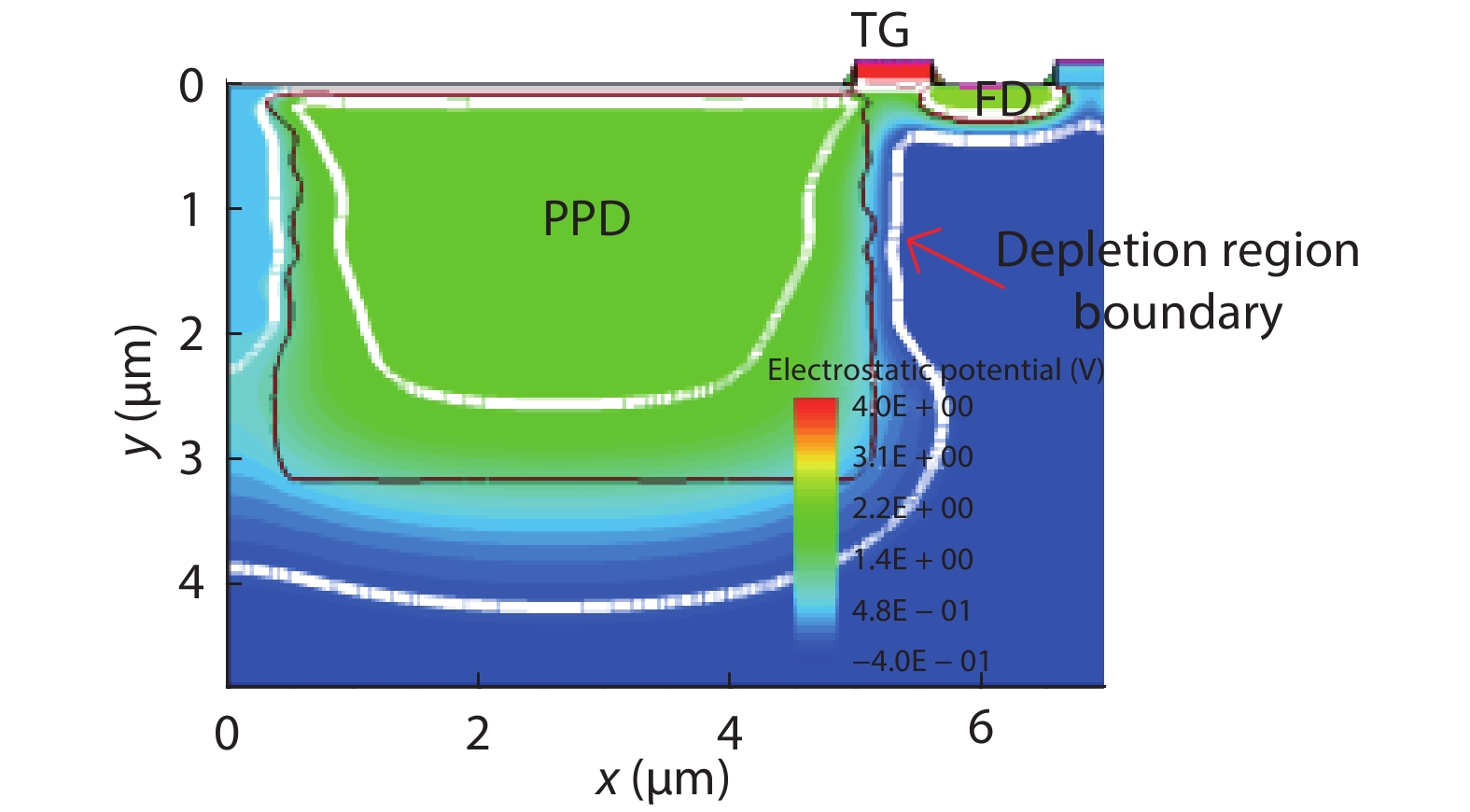
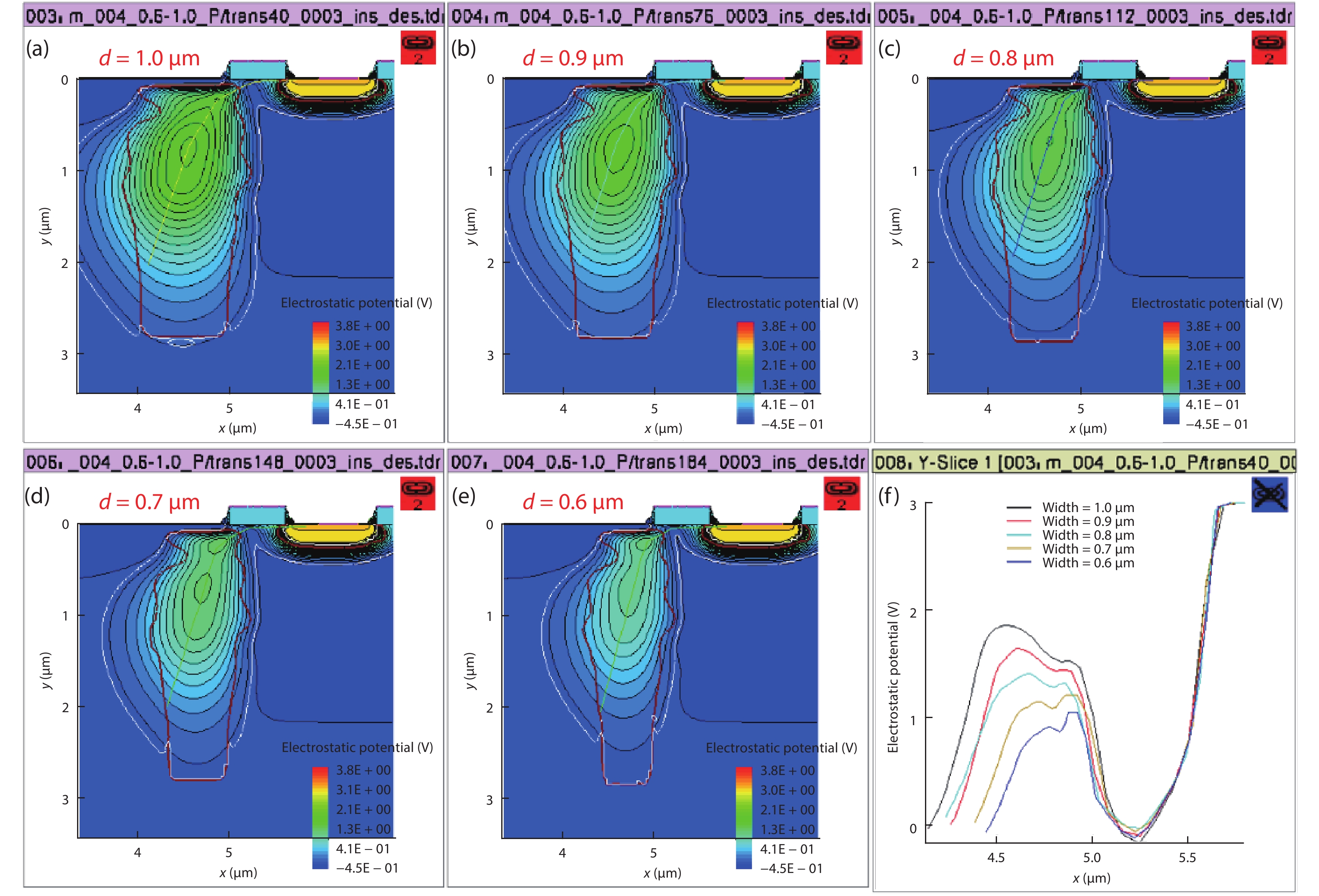
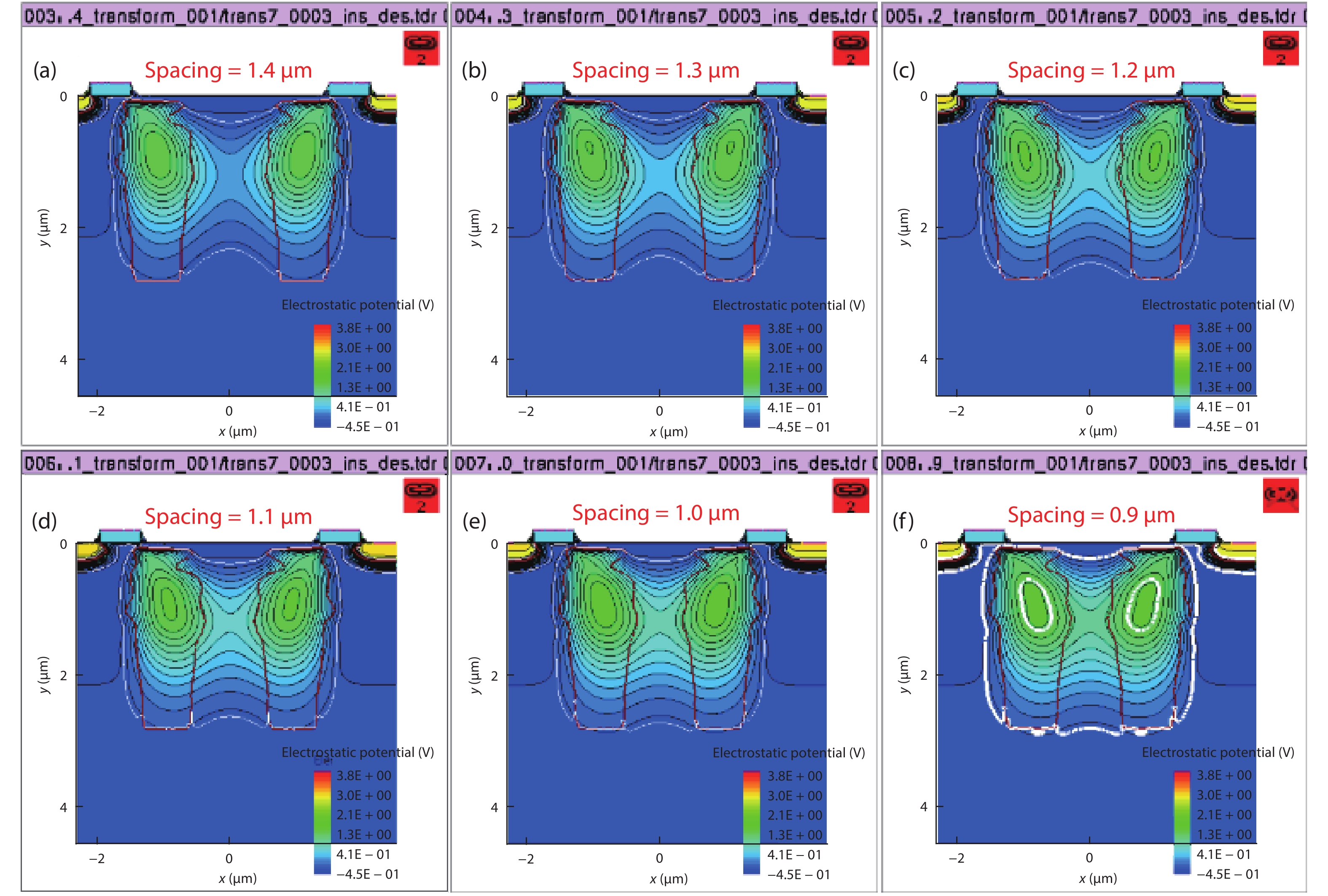
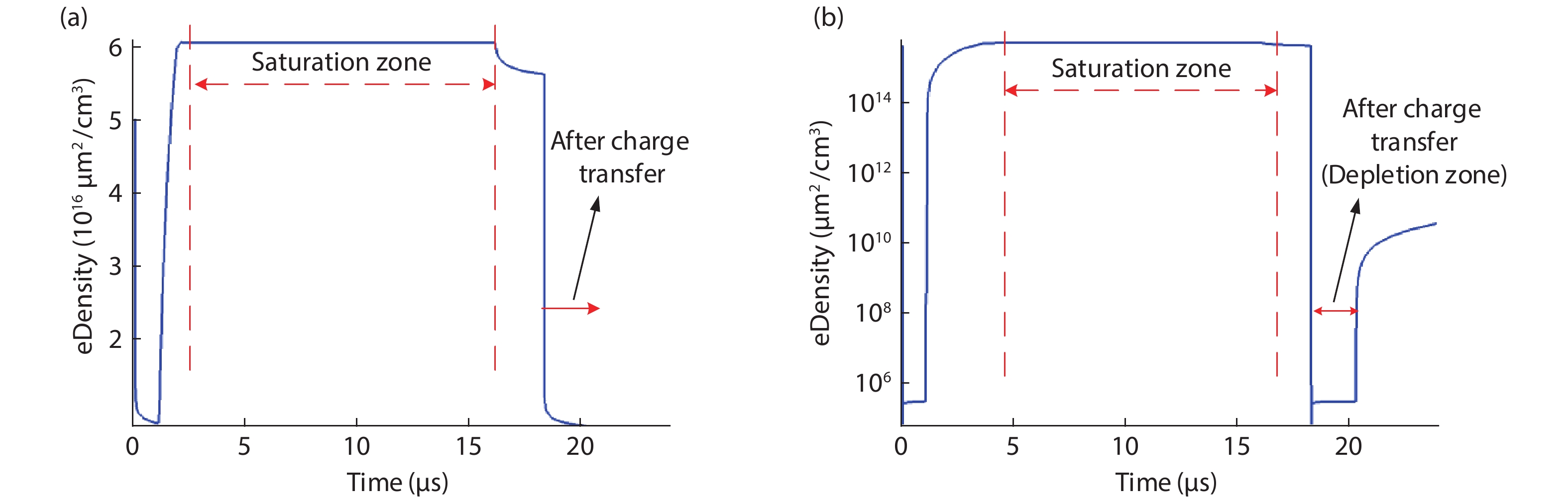
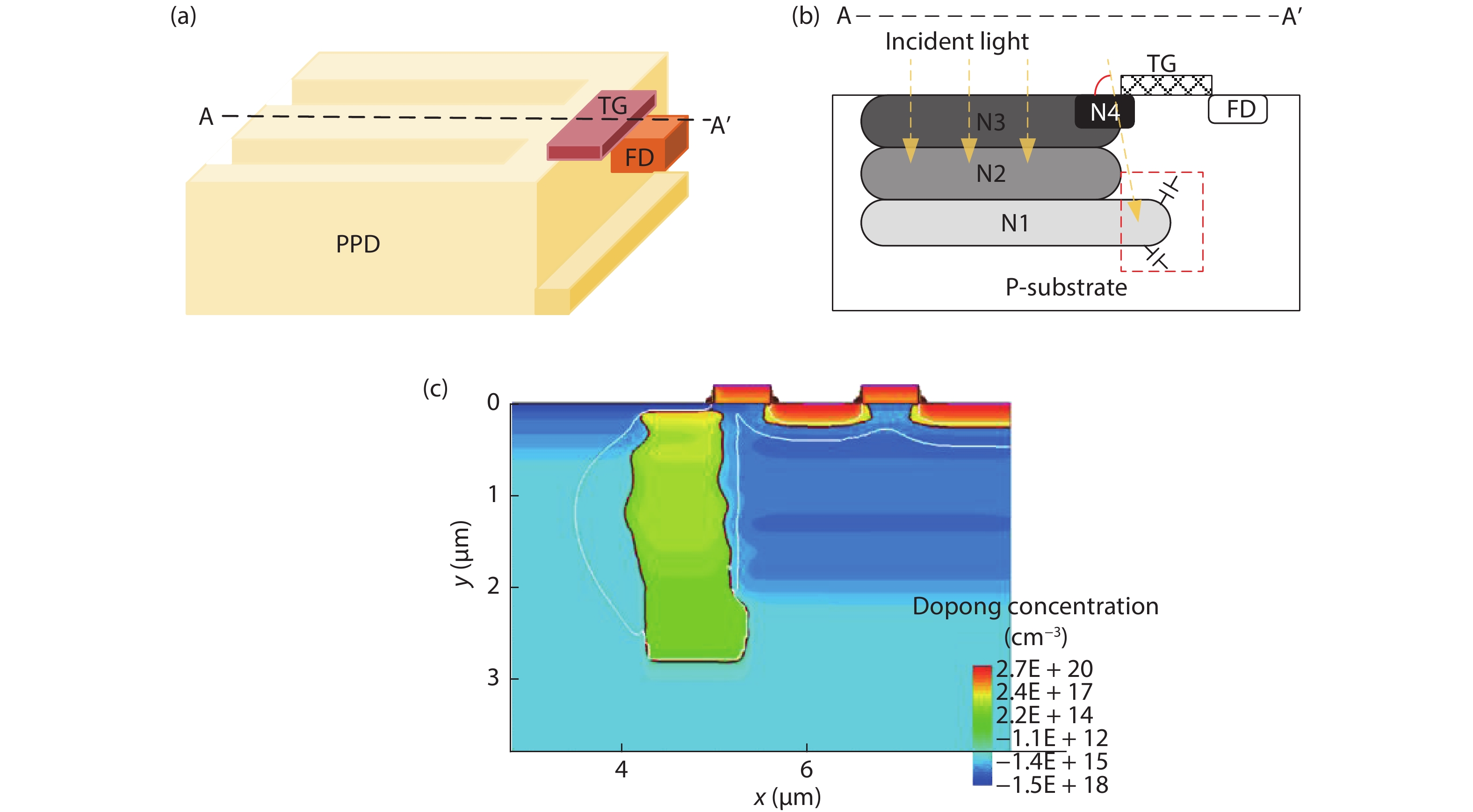
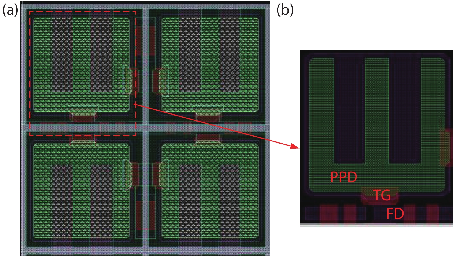

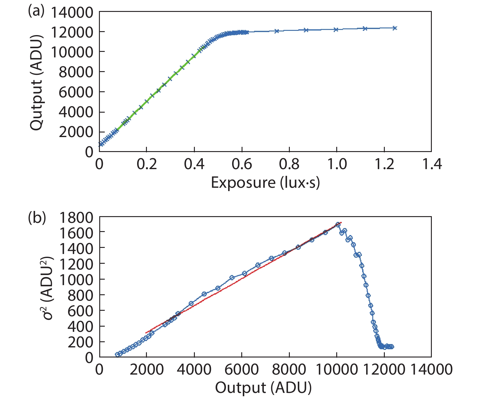
Table 1. Vpin, NFWC and depletion depth (W) with different d.
| d (μm) | 0.6 | 0.7 | 0.8 | 0.9 | 1.0 |
| Vpin (V) | 1.057 | 1.215 | 1.408 | 1.646 | 1.863 |
| NFWC (e–) | 3094 | 4335 | 5516 | 6725 | 7966 |
| W (μm) | 2.842 | 2.792 | 2.845 | 2.845 | 2.845 |
 DownLoad: CSV
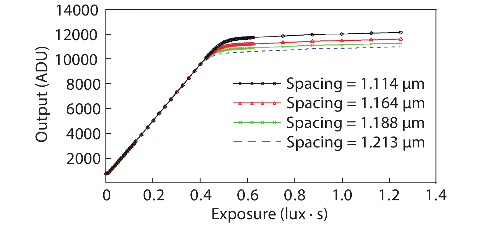
Table 2. Vpin with different PPD spacing.
| Spacing (μm) | 1.4 | 1.3 | 1.2 | 1.1 | 1.0 | 0.9 |
| Vpin (V) | 1.382 | 1.415 | 1.424 | 1.438 | 1.506 | Not fully depleted |
DownLoad: CSV
Table 3. Performance comparison between the pixel test results with a PPD of finger shape and related literature.
DownLoad: CSV
| [1] |
Bigas M, Cabruja E, Forest J, et al. Review of CMOS image sensor. Microelectron J, 2006, 37(5), 433 doi: 10.1016/j.mejo.2005.07.002
|
| [2] |
Luo B, Yang F X, Yan L. Key technologies and research development of CMOS image sensors. IITA International Conference on Geoscience and Remote Sensing, 2010, 322
|
| [3] |
Fontaine R. Innovative technology elements for large and small pixel CIS devices. Proc International Image Sensor Workshop (IISW), 2013, 1
|
| [4] |
Wang X D, Ye T. Comparative research and future tendency between CMOS and CCD image sensor. Electron Des Eng, 2010, 18(11), 184
|
| [5] |
Jan B, Erik J M, Wilco K, et al. Recent developments on large-area CCDs for professional applications. International image sensor workshop. Proc International Image Sensor Workshop (IISW), 2015, 1
|
| [6] |
Velichko S, Hynecek J, Johnson R, et al. CMOS global shutter charge storage pixels with improved performance. IEEE Trans Electron Devices, 2015, 63(1), 1 doi: 10.1109/TED.2015.2443495
|
| [7] |
Solhusvik J, Kuang J, Lin Z, et al. A comparison of high dynamic range CIS technologies for automotive applications. Proc International Image Sensor Workshop, 2013, 1
|
| [8] |
Freedman S D, Boussaid F. A high dynamic range CMOS image sensor with a novel pixel-level logarithmic counter memory. IEEE International Conference on Knowledge-Based Engineering and Innovation (KBEI), 2015, 14
|
| [9] |
Takayanagi I, Yoshimura N, Mori K, et al. An 87 dB single exposure dynamic range CMOS image sensor with a 3.0 μm triple conversion gain pixel. Proc International Image Sensor Workshop (IISW), 2017, 30
|
| [10] |
Wang R G, Yin Y X, Liang L, et al. A high dynamic range CMOS image sensor with dual charge transfer phase. IEEE International Conference on Solid-State and Integrated Circuit Technology (ICSICT), 2016, 1369
|
| [11] |
Yu J T, Li B Q, Yu P P, et al. Two-dimensional pixel image lag simulation and optimization in a 4-T CMOS image sensor. J Semicond, 2010, 31(9), 094011 doi: 10.1088/1674-4926/31/9/094011
|
| [12] |
Lofthouse-Smith D D, Soman M R, Allanwood E A H, et al. Image lag optimisation in a 4T CMOS image sensor for the JANUS camera on ESA's JUICE mission to Jupiter. Int Soc Opt Photonics, 2018, 10709, 107091J doi: 10.1117/12.2313686
|
| [13] |
Rizzolo S, Goiffon V, Estribeau M, et al. Influence of pixel design on charge transfer performances in CMOS image sensors. IEEE Trans Electron Devices, 2018, 65(3), 1048 doi: 10.1109/TED.2018.2790443
|
| [14] |
Orly Y P, Ran G, Yosi S D. A random access photodiode array for intelligent image capture. IEEE Trans Electron Devices, 1991, 38(8), 1772 doi: 10.1109/16.119013
|
| [15] |
Iltgen K, Bendel C, Benninghoven A. Optimized time-of-flight secondary ion mass spectroscopy depth profiling with a dual beam technique. J Vac Sci Technol A, 1997, 15(3), 460 doi: 10.1116/1.580874
|
| [16] |
Park Y H. Image sensor having self-aligned and overlapped photodiode and method of making same. US Patent 7180151, 2007
|
| [17] |
Li Z H. Research on image sensor with ultra wide dynamic range. PhD Thesis, Jilin University, 2016
|
| [18] |
Cao X, G?bler D, Lee C, et al. Design and optimisation of large 4T pixel. Proc Int Image Sensor Workshop (IISW), 2015, 112
|
| [19] |
Han L Q. Study on the charge transfer mechanism and noise of CMOS active pixel. PhD Thesis, Tianjin University, 2016
|
| [20] |
Oike Y, Akiyama K, Hung L D, et al. An 8.3M-pixel 480 fps global-shutter CMOS image sensor with gain-adaptive column ADCs and 2-on-1 stacked device structure. IEEE Symposium on VLSI Circuits, 2016, 1
|
| [21] |
Lim W, Hwang J, Kim D, et al. A low noise CMOS image sensor with a 14-bit two-step single-slope ADC and a column self-calibration technique. IEEE International Conference on Electronics, Circuits and Systems (ICECS), 2015, 51
|
| [22] |
Yeh S, Hsieh C. Novel single-slope ADC design for full well capacity expansion of CMOS image sensor. IEEE Sens J, 2013, 13(3), 1012 doi: 10.1109/JSEN.2012.2227706
|
| [23] |
Xu R, Ng W C, Yuan J, et al. A 1/2.5 inch VGA 400 fps CMOS image sensor with high sensitivity for machine vision. IEEE J Solid-State Circuits, 2014, 49(10), 2342 doi: 10.1109/JSSC.2014.2345018
|


Article views: 4278 Times PDF downloads: 152 Times Cited by: 0 Times
Received: 25 December 2019 Revised: 13 January 2020 Online: Accepted Manuscript: 10 April 2020Uncorrected proof: 21 April 2020Published: 01 October 2020
| Citation: |
Feng Li, Ruishuo Wang, Liqiang Han, Jiangtao Xu. Design of CMOS active pixels based on finger-shaped PPD[J]. Journal of Semiconductors, 2020, 41(10): 102301. doi: 10.1088/1674-4926/41/10/102301
****
F Li, R S Wang, L Q Han, J T Xu, Design of CMOS active pixels based on finger-shaped PPD[J]. J. Semicond., 2020, 41(10): 102301. doi: 10.1088/1674-4926/41/10/102301.

|
| [1] |
Bigas M, Cabruja E, Forest J, et al. Review of CMOS image sensor. Microelectron J, 2006, 37(5), 433 doi: 10.1016/j.mejo.2005.07.002
|
| [2] |
Luo B, Yang F X, Yan L. Key technologies and research development of CMOS image sensors. IITA International Conference on Geoscience and Remote Sensing, 2010, 322
|
| [3] |
Fontaine R. Innovative technology elements for large and small pixel CIS devices. Proc International Image Sensor Workshop (IISW), 2013, 1
|
| [4] |
Wang X D, Ye T. Comparative research and future tendency between CMOS and CCD image sensor. Electron Des Eng, 2010, 18(11), 184
|
| [5] |
Jan B, Erik J M, Wilco K, et al. Recent developments on large-area CCDs for professional applications. International image sensor workshop. Proc International Image Sensor Workshop (IISW), 2015, 1
|
| [6] |
Velichko S, Hynecek J, Johnson R, et al. CMOS global shutter charge storage pixels with improved performance. IEEE Trans Electron Devices, 2015, 63(1), 1 doi: 10.1109/TED.2015.2443495
|
| [7] |
Solhusvik J, Kuang J, Lin Z, et al. A comparison of high dynamic range CIS technologies for automotive applications. Proc International Image Sensor Workshop, 2013, 1
|
| [8] |
Freedman S D, Boussaid F. A high dynamic range CMOS image sensor with a novel pixel-level logarithmic counter memory. IEEE International Conference on Knowledge-Based Engineering and Innovation (KBEI), 2015, 14
|
| [9] |
Takayanagi I, Yoshimura N, Mori K, et al. An 87 dB single exposure dynamic range CMOS image sensor with a 3.0 μm triple conversion gain pixel. Proc International Image Sensor Workshop (IISW), 2017, 30
|
| [10] |
Wang R G, Yin Y X, Liang L, et al. A high dynamic range CMOS image sensor with dual charge transfer phase. IEEE International Conference on Solid-State and Integrated Circuit Technology (ICSICT), 2016, 1369
|
| [11] |
Yu J T, Li B Q, Yu P P, et al. Two-dimensional pixel image lag simulation and optimization in a 4-T CMOS image sensor. J Semicond, 2010, 31(9), 094011 doi: 10.1088/1674-4926/31/9/094011
|
| [12] |
Lofthouse-Smith D D, Soman M R, Allanwood E A H, et al. Image lag optimisation in a 4T CMOS image sensor for the JANUS camera on ESA's JUICE mission to Jupiter. Int Soc Opt Photonics, 2018, 10709, 107091J doi: 10.1117/12.2313686
|
| [13] |
Rizzolo S, Goiffon V, Estribeau M, et al. Influence of pixel design on charge transfer performances in CMOS image sensors. IEEE Trans Electron Devices, 2018, 65(3), 1048 doi: 10.1109/TED.2018.2790443
|
| [14] |
Orly Y P, Ran G, Yosi S D. A random access photodiode array for intelligent image capture. IEEE Trans Electron Devices, 1991, 38(8), 1772 doi: 10.1109/16.119013
|
| [15] |
Iltgen K, Bendel C, Benninghoven A. Optimized time-of-flight secondary ion mass spectroscopy depth profiling with a dual beam technique. J Vac Sci Technol A, 1997, 15(3), 460 doi: 10.1116/1.580874
|
| [16] |
Park Y H. Image sensor having self-aligned and overlapped photodiode and method of making same. US Patent 7180151, 2007
|
| [17] |
Li Z H. Research on image sensor with ultra wide dynamic range. PhD Thesis, Jilin University, 2016
|
| [18] |
Cao X, G?bler D, Lee C, et al. Design and optimisation of large 4T pixel. Proc Int Image Sensor Workshop (IISW), 2015, 112
|
| [19] |
Han L Q. Study on the charge transfer mechanism and noise of CMOS active pixel. PhD Thesis, Tianjin University, 2016
|
| [20] |
Oike Y, Akiyama K, Hung L D, et al. An 8.3M-pixel 480 fps global-shutter CMOS image sensor with gain-adaptive column ADCs and 2-on-1 stacked device structure. IEEE Symposium on VLSI Circuits, 2016, 1
|
| [21] |
Lim W, Hwang J, Kim D, et al. A low noise CMOS image sensor with a 14-bit two-step single-slope ADC and a column self-calibration technique. IEEE International Conference on Electronics, Circuits and Systems (ICECS), 2015, 51
|
| [22] |
Yeh S, Hsieh C. Novel single-slope ADC design for full well capacity expansion of CMOS image sensor. IEEE Sens J, 2013, 13(3), 1012 doi: 10.1109/JSEN.2012.2227706
|
| [23] |
Xu R, Ng W C, Yuan J, et al. A 1/2.5 inch VGA 400 fps CMOS image sensor with high sensitivity for machine vision. IEEE J Solid-State Circuits, 2014, 49(10), 2342 doi: 10.1109/JSSC.2014.2345018
|

 WeChat ID
Journal of Semiconductors © 2017 All Rights Reserved 京ICP備05085259號(hào)-2