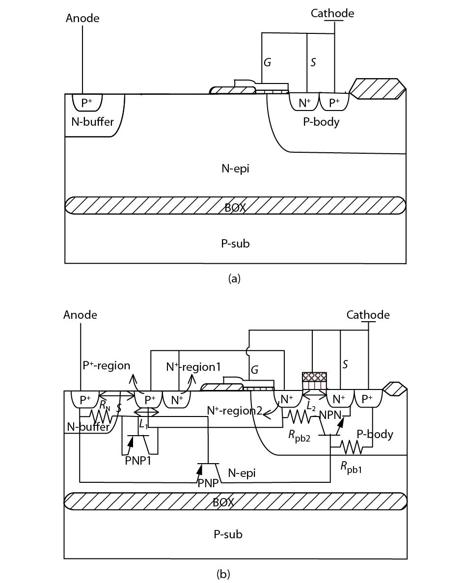
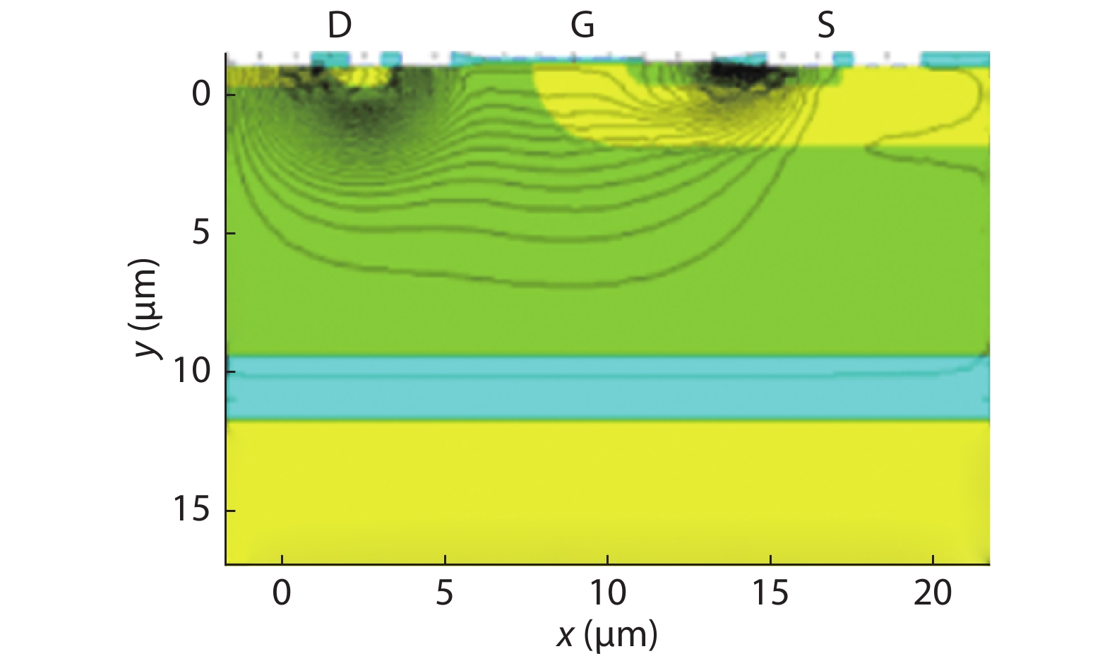
Fig. 1.
Cross-sectional view of (a) conventional LIGBT structure, (b) NTLIGBT structure.
ARTICLES
Li Tian, Jianbing Cheng, Cairong Zhang, Li Shen and Lei Wang
Corresponding author: Li Tian, 664138841@qq.com
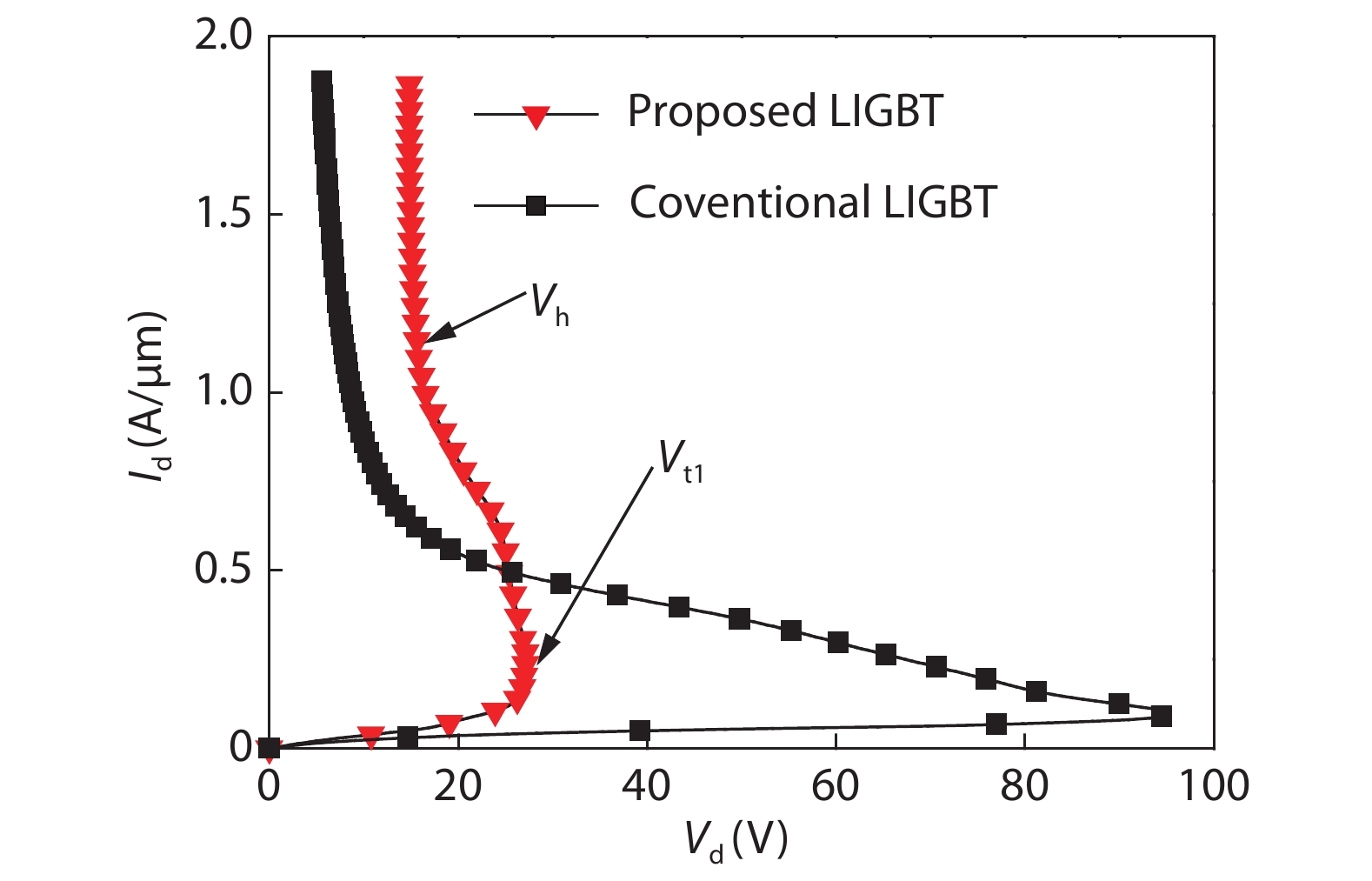
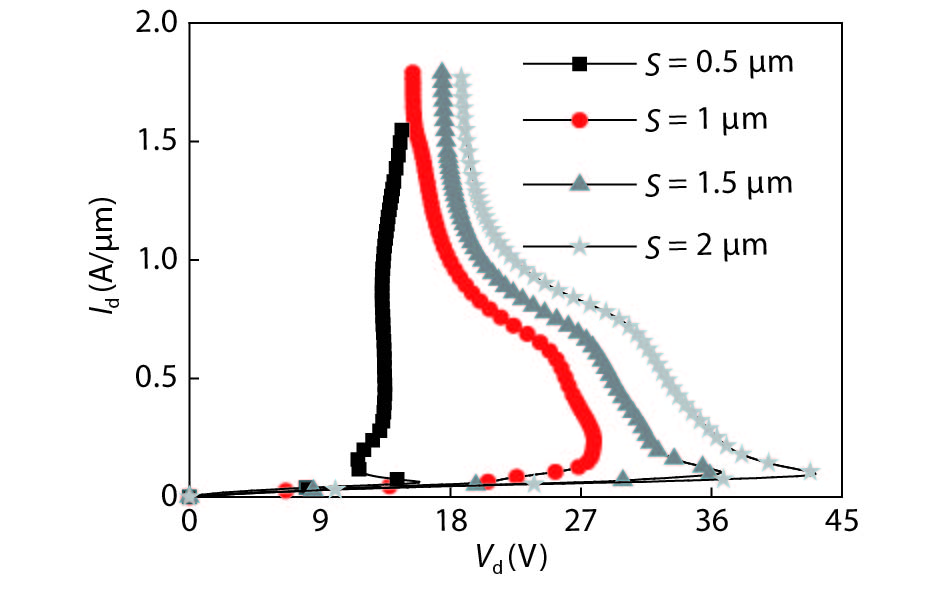
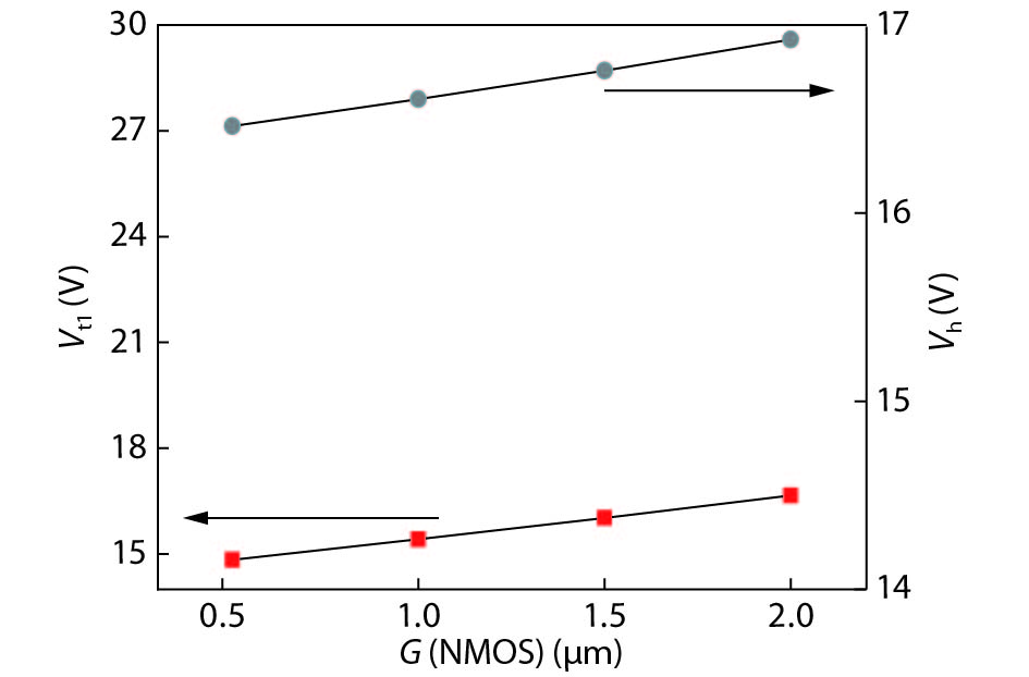
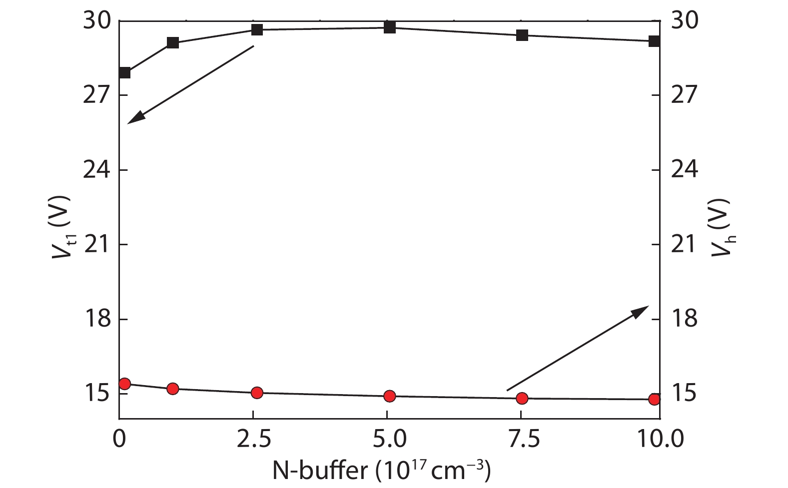
Abstract: A novel NMOS triggered LIGBT (NTLIGBT) structure is proposed for electrostatic discharge (ESD) protection in this paper. The structure utilizes internal NMOS to trigger SCR-like structure in LIGBT. The trigger voltage is significantly reduced because the embedded NMOS causes N+-drain/P-body junction being apt to avalanche breakdown. At the same time, the new parasitic PNP transistor including the newly added P+-region as a collector forms another path to bleed ESD current and then the conductivity modulation in the LIGBT is weakened. As a result, the holding voltage is increased. So, the proposed NTLIGBT structure has a narrow ESD design window. The simulation results show an improvement of 71.5% in trigger voltage and over 50% in holding voltage comparing with the conventional LIGBT structure.
Key words: ESD, NMOS triggered LIGBT (NTLIGBT), trigger voltage, holding voltage, ESD design window
| [1] |
Schaller R. Moore's law: past, present, and future. IEEE Spectrum, 1997, 34(6), 52 doi: 10.1109/6.591665
|
| [2] |
Vigna B. More than Moore: micro-machined products enable new applications and open new markets. International Electron Devices Meeting, 2005, 1
|
| [3] |
Cheng J B, Chen S S, Tian L. A new SCR-LDMOSFET embedded p- region for electrostatic discharge protection. IEEE International Power Electronics and Application Conference and Exposition, 2018, 1
|
| [4] |
Qian Q, Sun W, Wei S, et al. The investigation of electrothermal characteristics of high-voltage lateral IGBT for ESD protection. IEEE Trans Device Mater Reliab, 2012, 12(1), 146 doi: 10.1109/TDMR.2011.2178072
|
| [5] |
Arbess H, Tremouilles D, Bafleur M. High-temperature operation MOS-IGBT power clamp for improved ESD protection in smart power SOI technology. Electrical Overstress electrostatic Discharge Symposium, 2011, 1
|
| [6] |
Wu J, Dong S, Han Y, et al. Lateral IGBT in thin SOI process for high voltage ESD application. IEEE International Conference on Electron Devices and Solid-State Circuit, 2012, 1
|
| [7] |
Jiang L, Fan H, Qiao M, et al. ESD characterization of a 190 V LIGBT SOI ESD power clamp structure for plasma display panel applications. Microelectron Reliab, 2013, 53(5), 687 doi: 10.1016/j.microrel.2013.02.002
|
| [8] |
Qian Q, Liu S, Sun W, et al. A robust W-shape-buffer LIGBT device with large current capability. IEEE Trans Power Electron, 2014, 29(9), 4466 doi: 10.1109/TPEL.2014.2299822
|
| [9] |
Zeng J, Dong S, Liou J J, et al. Design and analysis of an area-efficient high holding voltage ESD protection device. IEEE Trans Electron Devices, 2015, 62(2), 606 doi: 10.1109/TED.2014.2381511
|
| [10] |
Ye R, Liu S, Sun W, et al. ESD robustness concern for SOI-LIGBTs with typical latch-up immunity structures. Solid State Electron, 2017, 137, 6 doi: 10.1016/j.sse.2017.07.010
|
| [11] |
Ye R, Liu S, Tian Y, et al. Influence of latch-up immunity structure on ESD robustness of SOI-LIGBT used as output device. IEEE Trans Device Mater Reliab, 2018, 18, 284 doi: 10.1109/TDMR.2018.2829550
|


Article views: 4171 Times PDF downloads: 54 Times Cited by: 0 Times
Received: 04 January 2019 Revised: 24 March 2019 Online: Accepted Manuscript: 09 April 2019Uncorrected proof: 11 April 2019Published: 08 May 2019
| Citation: |
Li Tian, Jianbing Cheng, Cairong Zhang, Li Shen, Lei Wang. Design and analysis of a NMOS triggered LIGBT structure for electrostatic discharge protection[J]. Journal of Semiconductors, 2019, 40(5): 052402. doi: 10.1088/1674-4926/40/5/052402
****
L Tian, J B Cheng, C R Zhang, L Shen, L Wang, Design and analysis of a NMOS triggered LIGBT structure for electrostatic discharge protection[J]. J. Semicond., 2019, 40(5): 052402. doi: 10.1088/1674-4926/40/5/052402.

|
| [1] |
Schaller R. Moore's law: past, present, and future. IEEE Spectrum, 1997, 34(6), 52 doi: 10.1109/6.591665
|
| [2] |
Vigna B. More than Moore: micro-machined products enable new applications and open new markets. International Electron Devices Meeting, 2005, 1
|
| [3] |
Cheng J B, Chen S S, Tian L. A new SCR-LDMOSFET embedded p- region for electrostatic discharge protection. IEEE International Power Electronics and Application Conference and Exposition, 2018, 1
|
| [4] |
Qian Q, Sun W, Wei S, et al. The investigation of electrothermal characteristics of high-voltage lateral IGBT for ESD protection. IEEE Trans Device Mater Reliab, 2012, 12(1), 146 doi: 10.1109/TDMR.2011.2178072
|
| [5] |
Arbess H, Tremouilles D, Bafleur M. High-temperature operation MOS-IGBT power clamp for improved ESD protection in smart power SOI technology. Electrical Overstress electrostatic Discharge Symposium, 2011, 1
|
| [6] |
Wu J, Dong S, Han Y, et al. Lateral IGBT in thin SOI process for high voltage ESD application. IEEE International Conference on Electron Devices and Solid-State Circuit, 2012, 1
|
| [7] |
Jiang L, Fan H, Qiao M, et al. ESD characterization of a 190 V LIGBT SOI ESD power clamp structure for plasma display panel applications. Microelectron Reliab, 2013, 53(5), 687 doi: 10.1016/j.microrel.2013.02.002
|
| [8] |
Qian Q, Liu S, Sun W, et al. A robust W-shape-buffer LIGBT device with large current capability. IEEE Trans Power Electron, 2014, 29(9), 4466 doi: 10.1109/TPEL.2014.2299822
|
| [9] |
Zeng J, Dong S, Liou J J, et al. Design and analysis of an area-efficient high holding voltage ESD protection device. IEEE Trans Electron Devices, 2015, 62(2), 606 doi: 10.1109/TED.2014.2381511
|
| [10] |
Ye R, Liu S, Sun W, et al. ESD robustness concern for SOI-LIGBTs with typical latch-up immunity structures. Solid State Electron, 2017, 137, 6 doi: 10.1016/j.sse.2017.07.010
|
| [11] |
Ye R, Liu S, Tian Y, et al. Influence of latch-up immunity structure on ESD robustness of SOI-LIGBT used as output device. IEEE Trans Device Mater Reliab, 2018, 18, 284 doi: 10.1109/TDMR.2018.2829550
|

 WeChat ID
Journal of Semiconductors © 2017 All Rights Reserved 京ICP備05085259號-2
 DownLoad: