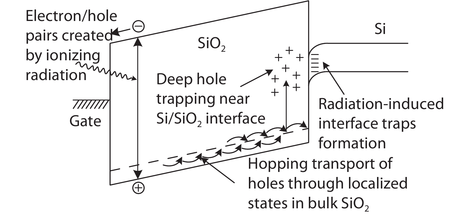
Fig. 1.
Band diagram for MOS structure with positive gate bias, indicating main processes for radiation-induced charge generation.
ARTICLES
Yanfei Li, Shaoli Zhu, Jianwei Wu, Genshen Hong and Zheng Xu
Corresponding author: Yanfei Li, Email: mama_1015@163.com
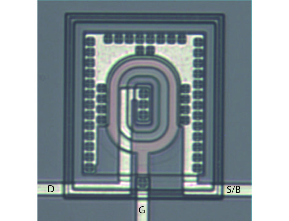
Abstract: Based on the silicon-on-insulator (SOI) technology and radiation-hardened silicon gate (RSG) process, a radiation-hardened high-voltage lateral double-diffused MOSFET (LDMOS) device is presented in this paper. With the gate supply voltage of 30 V, the LDMOS device has a gate oxide thickness of 120 nm, and the RSG process is effective in reducing the total ionizing dose (TID) radiation-induced threshold voltage shift. The p-type ion implantation process and gate-enclosed layout topology are used to prevent radiation-induced leakage current through a parasitic path under the bird's beak and at the deep trench corner, and the device is compatible with high-voltage SOI CMOS process. In the proposed LDMOS, the total ionizing dose radiation degradation for the ON bias is more sensitive than the OFF bias. The experiment results show that the SOI LDMOS has a negative threshold voltage shift of 1.12 V, breakdown voltage of 135 V, and off-state leakage current of 0.92 pA/μm at an accumulated dose level of 100 krad (Si).
Key words: radiation-hardened, RGS, total ion dose, threshold voltage shift
| [1] |
Ma T P, Dressendorfer P V. Ionizing radiation effects in MOS devices and circuits. New York: Wiley-Interscience,1989
|
| [2] |
Wang Y X, Hu R B, Li R Z, et al. Total dose effects on the matching properties of deep submicron MOS transistors. J Semicond, 2014, 35(6), 064007 doi: 10.1088/1674-4926/35/6/064007
|
| [3] |
Tang Zh H, Liu R K, Tan K Zh, et al. A novel terminal structure for total dose irradiation hardened of a P-VDMOS. J Semicond, 2014, 35(5), 054005 doi: 10.1088/1674-4926/35/5/054005
|
| [4] |
Zheng Y Zh, Lu W, Ren D Y, et al. Characteristics of high and low-dose-rate damage for domestic npn transistors of various emitter areas. Acta Physica Sinic, 2009, 58(8), 5572 doi: 10.7498/aps.58.5572
|
| [5] |
Zebrev G I, Drosdetsky M G, Galimov A M. Non-equilibrium carrier capture, recombination and annealing in thick insulators and their impact on radiation hardness. J Semicond, 2016, 37(11), 115001 doi: 10.1088/1674-4926/37/11/115001
|
| [6] |
McLain M L, Barnaby H J, Schlenvogt G. Effects of channel implant variation on radiation-induced edge leakage currents in n-channel MOSFETs. IEEE Trans Nucl Sci, 2017, 64(8), 2235 doi: 10.1109/TNS.2017.2705118
|
| [7] |
Shaneyfelt M R, Dodd P E, Draper B L, et al. Challenges in hardening technologies using shallow-trench isolation. IEEE Trans Nucl Sci, 1998, 45(6), 2584 doi: 10.1109/23.736501
|
| [8] |
Gaillardin M, Martinez M, Girard S, et al. High total ionizing dose and temperature effects on micro- and nano-electronic devices. IEEE Trans Nucl Sci, 2015, 62(3), 1226 doi: 10.1109/TNS.2015.2416975
|
| [9] |
Ding L L, Guo H X, Chen W, et al. Study of radiation-induced leakage current between adjacent devices in a CMOS integrated circuit. J Semicond, 2012, 33(6), 064006 doi: 10.1088/1674-4926/33/6/064006
|
| [10] |
He B P, Wang Z J, Sheng J K, et al. Total ionizing dose radiation effects on NMOS parasitic transistors in advanced bulk CMOS technology devices. J Semicond, 2016, 37(12), 124003 doi: 10.1088/1674-4926/37/12/124003
|
| [11] |
Jiang J, Shu W, Chong K S, et al. Total ionizing dose (TID) effects on finger transistors in a 65 nm CMOS process. IEEE International Symposium on Circuits and Systems, 2016, 5 doi: 10.1109/ISCAS.2016.7527156
|
| [12] |
Zhou X, Luo P, He L Y, et al. A radiation-hard waffle layout for BCD power MOSFET. IEEE 12th International Conference on ASIC, 2017, 773
|
| [13] |
Schwank J R, Ferlet-Cavrois V, Shaneyfelt M R, et al. Radiation effects in SOI technologies. IEEE Trans Nucl Sci, 2003, 50, 522 doi: 10.1109/TNS.2003.812930
|
| [14] |
Han X W, Wu L H, Zhao Y, et al. A radiation hardened SOI based FPGA. J Semicond, 2011, 32(7), 075012 doi: 10.1088/1674-4926/32/7/075012
|
| [15] |
Huang Y, Li B H, Zhao X, et al. An effective method to compensate total ionizing dose-induced degradation on double-SOI structure. IEEE Trans Nucl Sci, 2018, 65(8), 1532 doi: 10.1109/TNS.2018.2824402
|
| [16] |
Zhao K, Zhao X, Gao J T, et al. DSOI FET – A novel TID tolerant SOI transistor. IEEE International Conference on Solid-State and Integrated Circuit Technology, 2014, 1 doi: 10.1109/ICSICT.2014.7021440
|
| [17] |
Warren W L, Shaneyfelt M R, Fleetwood D M, at el. Microscopic nature of border traps in MOS devices. IEEE Trans Nucl Sci, 1994, 41, 1817 doi: 10.1109/23.340513
|
| [18] |
Fleetwood Daniel M. Evolution of total ionizing dose effects in MOS devices with Moore's Law scaling. IEEE Trans Nucl Sci, 2018, 65(8), 1465 doi: 10.1109/TNS.2017.2786140
|
| [19] |
Schwank J R, Albuquerque N M, Shaneyfelt M R, et al. Radiation effects in MOS oxides. IEEE Trans Nucl Sci, 2008, 55(4), 1833 doi: 10.1109/TNS.2008.2001040
|
| [20] |
Cai X W, Hai Ch H, Wang L X, et al. Gamma irradiation induced oxide trapped charge and interface charge in power VDMOS. J Funct Mater Devices, 2008, 14(5), 621 doi: 10.3969/j.issn.1007-4252.2008.05.015
|
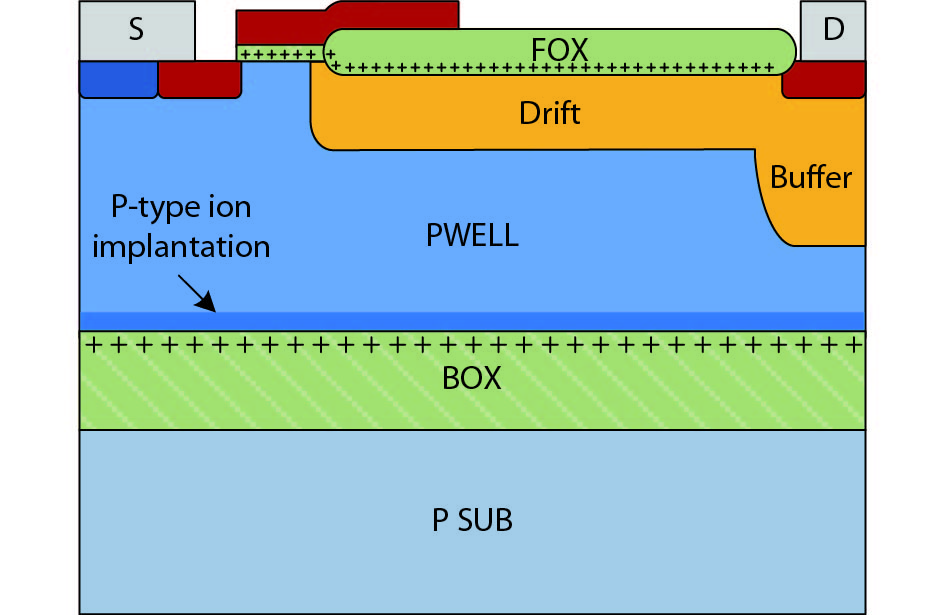
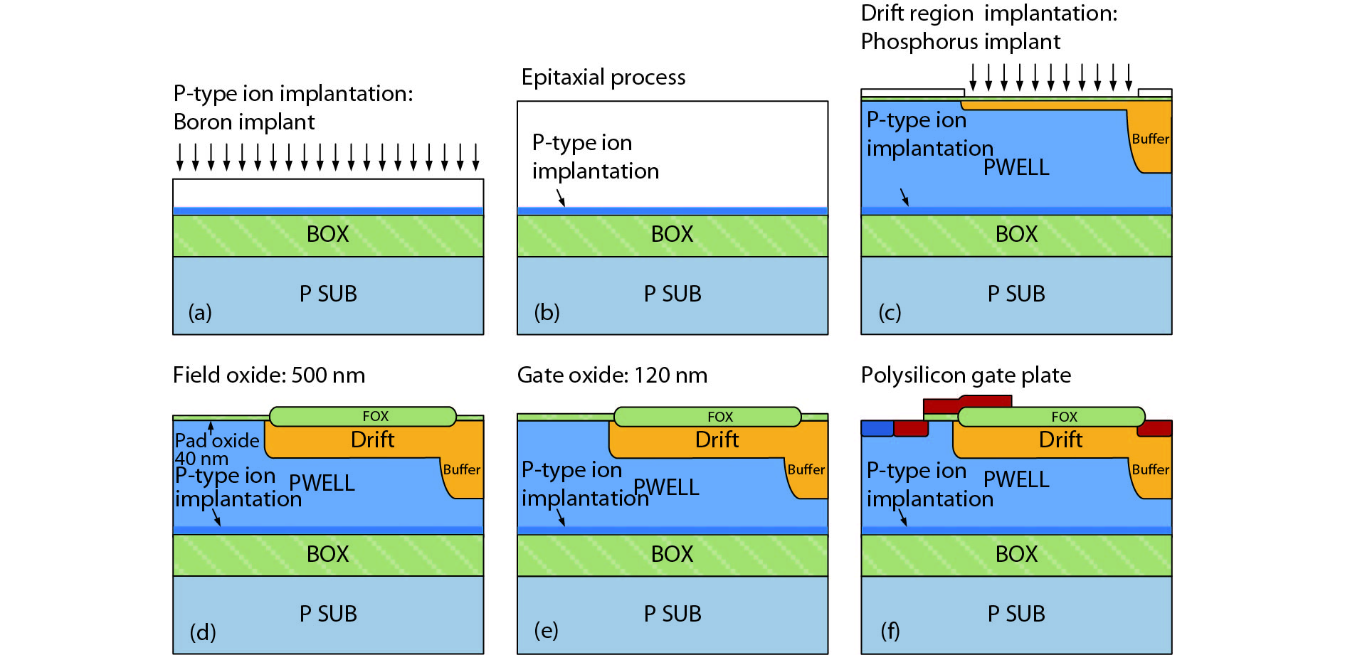
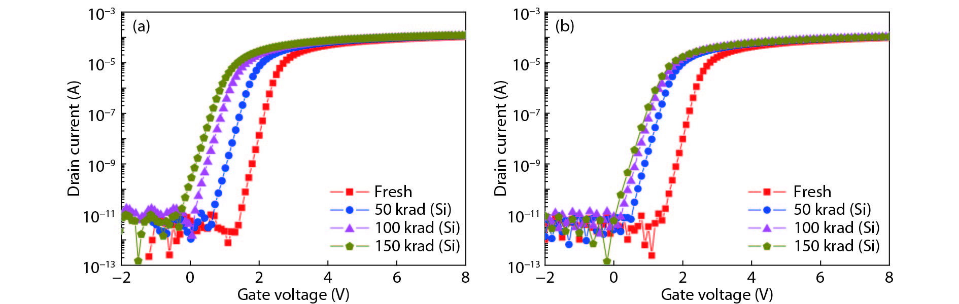
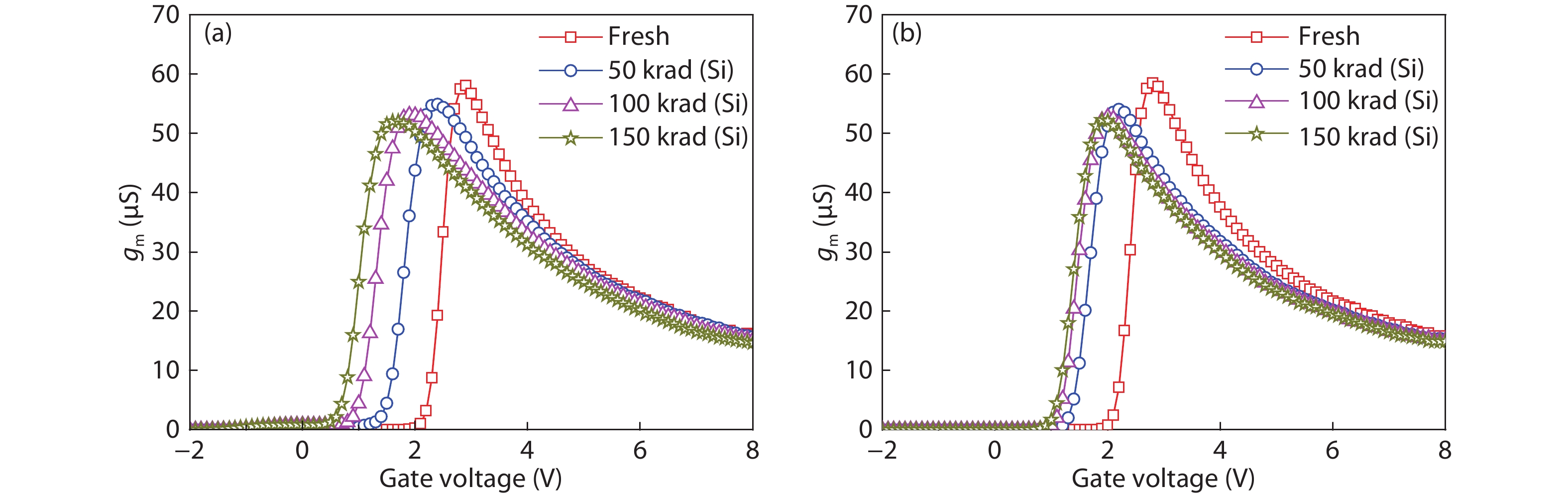
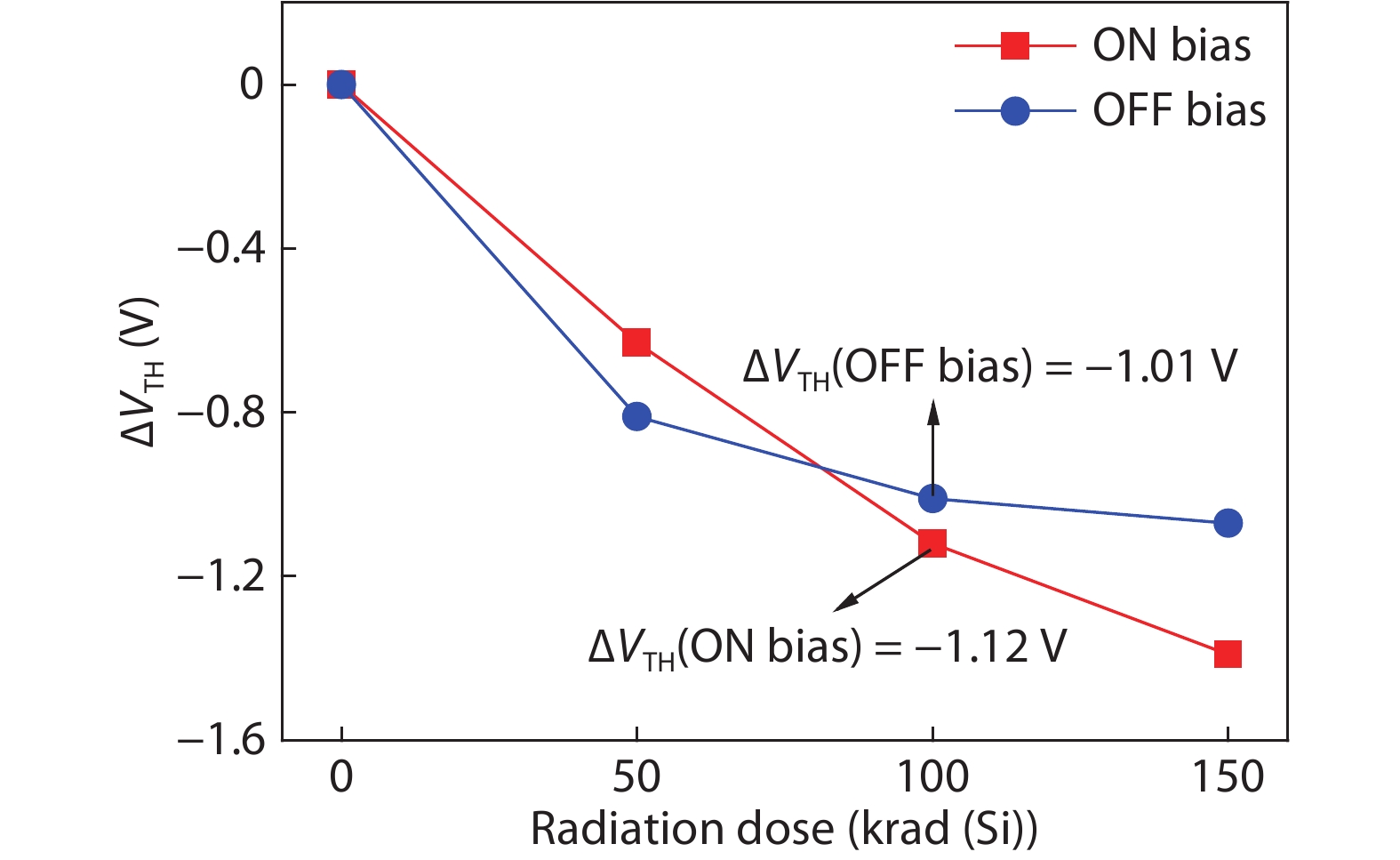
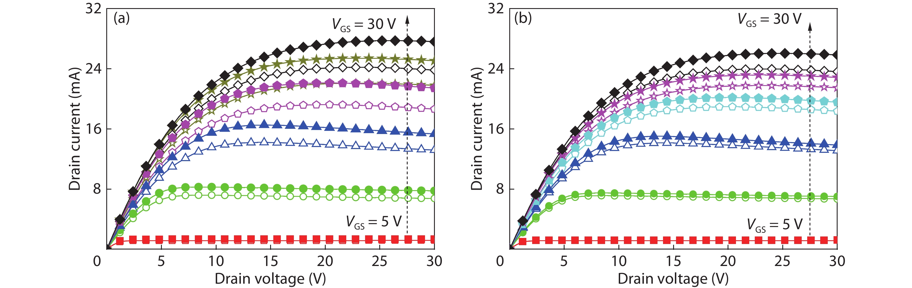
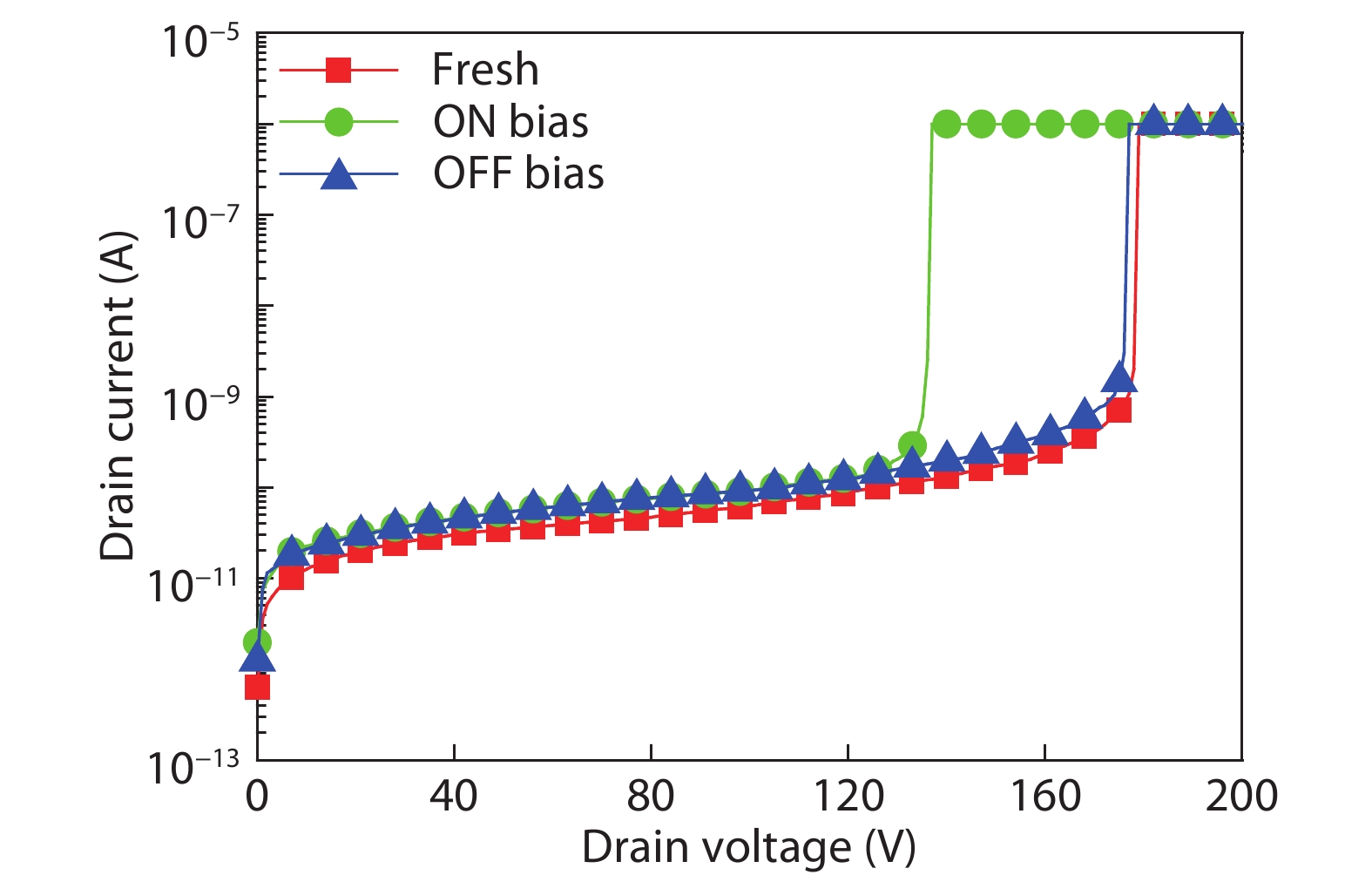
Table 1. Values of main structure parameters for the proposed SOI LDMOS device.
| Parameter | Value |
| Gate oxide thickness | 120 nm |
| The thickness of p-type epitaxial film | 8 μm |
| The thickness of buried oxide layer | 3 μm |
| The resistivity of p-type epitaxial film | 10–20 Ω·cm |
| Width/length | 100 μm/4 μm |
| Device structure | Gate-enclosed layout |
 DownLoad: CSV
Table 2. Bias conditions definition.
| Bias state | VD (V) | VG (V) | VBS (V) | VSUB (V) |
| ON bias | 0 | 30 | 0 | 0 |
| OFF bias | 100 | 0 | 0 | 0 |
DownLoad: CSV
| [1] |
Ma T P, Dressendorfer P V. Ionizing radiation effects in MOS devices and circuits. New York: Wiley-Interscience,1989
|
| [2] |
Wang Y X, Hu R B, Li R Z, et al. Total dose effects on the matching properties of deep submicron MOS transistors. J Semicond, 2014, 35(6), 064007 doi: 10.1088/1674-4926/35/6/064007
|
| [3] |
Tang Zh H, Liu R K, Tan K Zh, et al. A novel terminal structure for total dose irradiation hardened of a P-VDMOS. J Semicond, 2014, 35(5), 054005 doi: 10.1088/1674-4926/35/5/054005
|
| [4] |
Zheng Y Zh, Lu W, Ren D Y, et al. Characteristics of high and low-dose-rate damage for domestic npn transistors of various emitter areas. Acta Physica Sinic, 2009, 58(8), 5572 doi: 10.7498/aps.58.5572
|
| [5] |
Zebrev G I, Drosdetsky M G, Galimov A M. Non-equilibrium carrier capture, recombination and annealing in thick insulators and their impact on radiation hardness. J Semicond, 2016, 37(11), 115001 doi: 10.1088/1674-4926/37/11/115001
|
| [6] |
McLain M L, Barnaby H J, Schlenvogt G. Effects of channel implant variation on radiation-induced edge leakage currents in n-channel MOSFETs. IEEE Trans Nucl Sci, 2017, 64(8), 2235 doi: 10.1109/TNS.2017.2705118
|
| [7] |
Shaneyfelt M R, Dodd P E, Draper B L, et al. Challenges in hardening technologies using shallow-trench isolation. IEEE Trans Nucl Sci, 1998, 45(6), 2584 doi: 10.1109/23.736501
|
| [8] |
Gaillardin M, Martinez M, Girard S, et al. High total ionizing dose and temperature effects on micro- and nano-electronic devices. IEEE Trans Nucl Sci, 2015, 62(3), 1226 doi: 10.1109/TNS.2015.2416975
|
| [9] |
Ding L L, Guo H X, Chen W, et al. Study of radiation-induced leakage current between adjacent devices in a CMOS integrated circuit. J Semicond, 2012, 33(6), 064006 doi: 10.1088/1674-4926/33/6/064006
|
| [10] |
He B P, Wang Z J, Sheng J K, et al. Total ionizing dose radiation effects on NMOS parasitic transistors in advanced bulk CMOS technology devices. J Semicond, 2016, 37(12), 124003 doi: 10.1088/1674-4926/37/12/124003
|
| [11] |
Jiang J, Shu W, Chong K S, et al. Total ionizing dose (TID) effects on finger transistors in a 65 nm CMOS process. IEEE International Symposium on Circuits and Systems, 2016, 5 doi: 10.1109/ISCAS.2016.7527156
|
| [12] |
Zhou X, Luo P, He L Y, et al. A radiation-hard waffle layout for BCD power MOSFET. IEEE 12th International Conference on ASIC, 2017, 773
|
| [13] |
Schwank J R, Ferlet-Cavrois V, Shaneyfelt M R, et al. Radiation effects in SOI technologies. IEEE Trans Nucl Sci, 2003, 50, 522 doi: 10.1109/TNS.2003.812930
|
| [14] |
Han X W, Wu L H, Zhao Y, et al. A radiation hardened SOI based FPGA. J Semicond, 2011, 32(7), 075012 doi: 10.1088/1674-4926/32/7/075012
|
| [15] |
Huang Y, Li B H, Zhao X, et al. An effective method to compensate total ionizing dose-induced degradation on double-SOI structure. IEEE Trans Nucl Sci, 2018, 65(8), 1532 doi: 10.1109/TNS.2018.2824402
|
| [16] |
Zhao K, Zhao X, Gao J T, et al. DSOI FET – A novel TID tolerant SOI transistor. IEEE International Conference on Solid-State and Integrated Circuit Technology, 2014, 1 doi: 10.1109/ICSICT.2014.7021440
|
| [17] |
Warren W L, Shaneyfelt M R, Fleetwood D M, at el. Microscopic nature of border traps in MOS devices. IEEE Trans Nucl Sci, 1994, 41, 1817 doi: 10.1109/23.340513
|
| [18] |
Fleetwood Daniel M. Evolution of total ionizing dose effects in MOS devices with Moore's Law scaling. IEEE Trans Nucl Sci, 2018, 65(8), 1465 doi: 10.1109/TNS.2017.2786140
|
| [19] |
Schwank J R, Albuquerque N M, Shaneyfelt M R, et al. Radiation effects in MOS oxides. IEEE Trans Nucl Sci, 2008, 55(4), 1833 doi: 10.1109/TNS.2008.2001040
|
| [20] |
Cai X W, Hai Ch H, Wang L X, et al. Gamma irradiation induced oxide trapped charge and interface charge in power VDMOS. J Funct Mater Devices, 2008, 14(5), 621 doi: 10.3969/j.issn.1007-4252.2008.05.015
|


Article views: 4669 Times PDF downloads: 130 Times Cited by: 0 Times
Received: 06 October 2018 Revised: 21 March 2019 Online: Accepted Manuscript: 04 April 2019Uncorrected proof: 09 April 2019Published: 08 May 2019
| Citation: |
Yanfei Li, Shaoli Zhu, Jianwei Wu, Genshen Hong, Zheng Xu. Research for radiation-hardened high-voltage SOI LDMOS[J]. Journal of Semiconductors, 2019, 40(5): 052401. doi: 10.1088/1674-4926/40/5/052401
****
Y F Li, S L Zhu, J W Wu, G S Hong, Z Xu, Research for radiation-hardened high-voltage SOI LDMOS[J]. J. Semicond., 2019, 40(5): 052401. doi: 10.1088/1674-4926/40/5/052401.

|
| [1] |
Ma T P, Dressendorfer P V. Ionizing radiation effects in MOS devices and circuits. New York: Wiley-Interscience,1989
|
| [2] |
Wang Y X, Hu R B, Li R Z, et al. Total dose effects on the matching properties of deep submicron MOS transistors. J Semicond, 2014, 35(6), 064007 doi: 10.1088/1674-4926/35/6/064007
|
| [3] |
Tang Zh H, Liu R K, Tan K Zh, et al. A novel terminal structure for total dose irradiation hardened of a P-VDMOS. J Semicond, 2014, 35(5), 054005 doi: 10.1088/1674-4926/35/5/054005
|
| [4] |
Zheng Y Zh, Lu W, Ren D Y, et al. Characteristics of high and low-dose-rate damage for domestic npn transistors of various emitter areas. Acta Physica Sinic, 2009, 58(8), 5572 doi: 10.7498/aps.58.5572
|
| [5] |
Zebrev G I, Drosdetsky M G, Galimov A M. Non-equilibrium carrier capture, recombination and annealing in thick insulators and their impact on radiation hardness. J Semicond, 2016, 37(11), 115001 doi: 10.1088/1674-4926/37/11/115001
|
| [6] |
McLain M L, Barnaby H J, Schlenvogt G. Effects of channel implant variation on radiation-induced edge leakage currents in n-channel MOSFETs. IEEE Trans Nucl Sci, 2017, 64(8), 2235 doi: 10.1109/TNS.2017.2705118
|
| [7] |
Shaneyfelt M R, Dodd P E, Draper B L, et al. Challenges in hardening technologies using shallow-trench isolation. IEEE Trans Nucl Sci, 1998, 45(6), 2584 doi: 10.1109/23.736501
|
| [8] |
Gaillardin M, Martinez M, Girard S, et al. High total ionizing dose and temperature effects on micro- and nano-electronic devices. IEEE Trans Nucl Sci, 2015, 62(3), 1226 doi: 10.1109/TNS.2015.2416975
|
| [9] |
Ding L L, Guo H X, Chen W, et al. Study of radiation-induced leakage current between adjacent devices in a CMOS integrated circuit. J Semicond, 2012, 33(6), 064006 doi: 10.1088/1674-4926/33/6/064006
|
| [10] |
He B P, Wang Z J, Sheng J K, et al. Total ionizing dose radiation effects on NMOS parasitic transistors in advanced bulk CMOS technology devices. J Semicond, 2016, 37(12), 124003 doi: 10.1088/1674-4926/37/12/124003
|
| [11] |
Jiang J, Shu W, Chong K S, et al. Total ionizing dose (TID) effects on finger transistors in a 65 nm CMOS process. IEEE International Symposium on Circuits and Systems, 2016, 5 doi: 10.1109/ISCAS.2016.7527156
|
| [12] |
Zhou X, Luo P, He L Y, et al. A radiation-hard waffle layout for BCD power MOSFET. IEEE 12th International Conference on ASIC, 2017, 773
|
| [13] |
Schwank J R, Ferlet-Cavrois V, Shaneyfelt M R, et al. Radiation effects in SOI technologies. IEEE Trans Nucl Sci, 2003, 50, 522 doi: 10.1109/TNS.2003.812930
|
| [14] |
Han X W, Wu L H, Zhao Y, et al. A radiation hardened SOI based FPGA. J Semicond, 2011, 32(7), 075012 doi: 10.1088/1674-4926/32/7/075012
|
| [15] |
Huang Y, Li B H, Zhao X, et al. An effective method to compensate total ionizing dose-induced degradation on double-SOI structure. IEEE Trans Nucl Sci, 2018, 65(8), 1532 doi: 10.1109/TNS.2018.2824402
|
| [16] |
Zhao K, Zhao X, Gao J T, et al. DSOI FET – A novel TID tolerant SOI transistor. IEEE International Conference on Solid-State and Integrated Circuit Technology, 2014, 1 doi: 10.1109/ICSICT.2014.7021440
|
| [17] |
Warren W L, Shaneyfelt M R, Fleetwood D M, at el. Microscopic nature of border traps in MOS devices. IEEE Trans Nucl Sci, 1994, 41, 1817 doi: 10.1109/23.340513
|
| [18] |
Fleetwood Daniel M. Evolution of total ionizing dose effects in MOS devices with Moore's Law scaling. IEEE Trans Nucl Sci, 2018, 65(8), 1465 doi: 10.1109/TNS.2017.2786140
|
| [19] |
Schwank J R, Albuquerque N M, Shaneyfelt M R, et al. Radiation effects in MOS oxides. IEEE Trans Nucl Sci, 2008, 55(4), 1833 doi: 10.1109/TNS.2008.2001040
|
| [20] |
Cai X W, Hai Ch H, Wang L X, et al. Gamma irradiation induced oxide trapped charge and interface charge in power VDMOS. J Funct Mater Devices, 2008, 14(5), 621 doi: 10.3969/j.issn.1007-4252.2008.05.015
|

 WeChat ID
Journal of Semiconductors © 2017 All Rights Reserved 京ICP備05085259號-2