


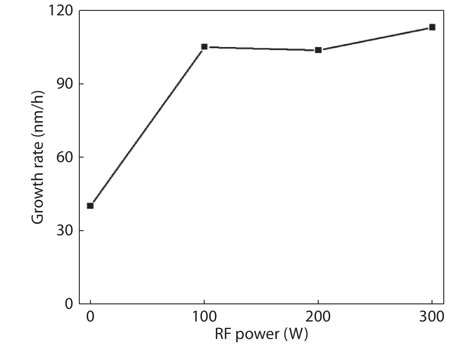
Fig. 1.
Dependence of growth rate of film on plasma RF power ranged from 0 to 300 W at substrate temperature of 500 °C.
ARTICLES
Congyu Hu, Katsuhiko Saito, Tooru Tanaka and Qixin Guo
Corresponding author: Qixin Guo, E-mail address: guoq@cc.saga-u.ac.jp (Qixin Guo)
Abstract: Gallium oxide was deposited on a c-plane sapphire substrate by oxygen plasma-assisted pulsed laser deposition (PLD). An oxygen radical was generated by an inductive coupled plasma source and the effect of radio frequency (RF) power on growth rate was investigated. A film grown with plasma assistance showed 2.7 times faster growth rate. X-ray diffraction and Raman spectroscopy analysis showed β-Ga2O3 films grown with plasma assistance at 500 °C. The roughness of the films decreased when the RF power of plasma treatment increased. Transmittance of these films was at least 80% and showed sharp absorption edge at 250 nm which was consistent with data previously reported.
Key words: wide bandgap, gallium oxide, oxygen radical, pulsed laser deposition, plasma
| [1] |
Huang C Y, Horng R H, Wuu D S, et al. Thermal annealing effect on material characterizations of β-Ga2O3 epilayer grown by metal organic chemical vapor deposition. Appl Phys Lett, 2013, 102, 011119 doi: 10.1063/1.4773247
|
| [2] |
Roy R, Hill V G, Osborn E F. Polymorphism of Ga2O3 and the system Ga2O3–H2O. J Am Chem Soc, 1952, 74(3), 719 doi: 10.1021/ja01123a039
|
| [3] |
Binet L, Gourier D. Origin of the blue luminescence of β-Ga2O3. J Phys Chem Solids, 1998, 59(8), 1241 doi: 10.1016/S0022-3697(98)00047-X
|
| [4] |
Kokubun Y, Miura K, Endo F, et al. Sol-gel prepared β-Ga2O3 thin films for ultraviolet photodetectors. Appl Phys Lett, 2007, 90(3), 8 doi: 10.1063/1.2432946
|
| [5] |
Oshima T, Okuno T, Arai N, et al. Vertical solar-blind deep-ultraviolet schottky photodetectors based on β- Ga2O3substrates. Appl Phys Express, 2008, 1(1), 011202 doi: 10.1143/APEX.1.011202
|
| [6] |
Orita M, Ohta H, Hirano M, et al. Deep-ultraviolet transparent conductive β-Ga2O3 thin films. Appl Phys Lett, 2000, 77(25), 4166 doi: 10.1063/1.1330559
|
| [7] |
Orita M, Hiramatsu H, Ohta H, et al. Preparation of highly conductive, deep ultraviolet transparent β-Ga2O3 thin film at low deposition temperatures. Thin Solid Films, 2002, 411(1), 134 doi: 10.1016/S0040-6090(02)00202-X
|
| [8] |
Higashiwaki M, Sasaki K, Kamimura T, et al. Depletion-mode Ga2O3 metal-oxide-semiconductor field-effect transistors on β-Ga2O3 (010) substrates and temperature dependence of their device characteristics. Appl Phys Lett, 2013, 103(12), 123511 doi: 10.1063/1.4821858
|
| [9] |
Lee S A, Hwang J Y, Kim J P, et al. Dielectric characterization of transparent epitaxial Ga2O3 thin film on n-GaN∕Al2O3 prepared by pulsed laser deposition. Appl Phys Lett, 2006, 89(18), 182906 doi: 10.1063/1.2374806
|
| [10] |
Matsuzaki K, Yanagi H, Kamiya T, et al. Field-induced current modulation in epitaxial film of deep-ultraviolet transparent oxide semiconductor Ga2O3. Appl Phys Lett, 2006, 88(9), 092106 doi: 10.1063/1.2179373
|
| [11] |
Oshima T, Okuno T, Fujita S. Ga2O3 thin film growth on c-plane sapphire substrates by molecular beam epitaxy for deep-ultraviolet photodetectors. Jpn J Appl Phys, 2007, 46, 7217 doi: 10.1143/JJAP.46.7217
|
| [12] |
Oshima T, Arai N, Suzuki N, et al. Surface morphology of homoepitaxial β-Ga2O3 thin films grown by molecular beam epitaxy. Thin Solid Films, 2008, 516(17), 5768 doi: 10.1016/j.tsf.2007.10.045
|
| [13] |
Zhang F B, Saito K, Tanaka T, et al. Structural and optical properties of Ga2O3 films on sapphire substrates by pulsed laser deposition. J Cryst Growth, 2014, 387, 96 doi: 10.1016/j.jcrysgro.2013.11.022
|
| [14] |
Fleischer M, Hanrieder W, Meixner H. Stability of semiconducting gallium oxide thin films. Thin Solid Films, 1990, 190(1), 93 doi: 10.1016/0040-6090(90)90132-W
|
| [15] |
Liu J J, Yan J L, Shi L, et al. Electrical and optical properties of deep ultraviolet transparent conductive Ga2O3/ITO films by magnetron sputtering. J Semicond, 2010, 31(10), 103001 doi: 10.1088/1674-4926/31/10/103001
|
| [16] |
Shinohara D, Fujita S. Heteroepitaxy of corundum-structured α-Ga2O3 thin films on α-Al2O3 substrates by ultrasonic mist chemical vapor deposition. Jpn J Appl Phys, 2008, 47, 731 doi: 10.1143/JJAP.47.7311
|
| [17] |
Murakami H, Nomura K, Goto K, et al. Homoepitaxial growth of β-Ga2O3 layers by halide vapor phase epitaxy. Appl Phys Express, 2015, 8(1), 015503 doi: 10.7567/APEX.8.015503
|
| [18] |
Zhang F, Arita M, Wang X, et al. Toward controlling the carrier density of Si doped Ga2O3 films by pulsed laser deposition. Appl Phys Lett, 2016, 109(10), 102105 doi: 10.1063/1.4962463
|
| [19] |
Matsubara K, Fons P, Iwata K, et al. Room-temperature deposition of Al-doped ZnO films by oxygen radical-assisted pulsed laser deposition. Thin Solid Films, 2002, 422(1/2), 176 doi: 10.1016/S0040-6090(02)00965-3
|
| [20] |
Kakehi Y, Okamoto A, Sakurai Y, et al. Epitaxial growth of LiNbO3 thin films using pulsed laser deposition. Appl Surf Sci, 2001, 169/170(1/2), 560 doi: 10.1016/S0169-4332(00)00739-X
|
| [21] |
Oh M S, Hwang D K, Seong D J, et al. Improvement of characteristics of Ga-doped ZnO grown by pulsed laser deposition using plasma-enhanced oxygen radicals. J Electrochem Soc, 2008, 155(9), D599 doi: 10.1149/1.2952077
|
| [22] |
He X, Wu J, Zhao L, et al. Synthesis and optical properties of tantalum oxide films prepared by ionized plasma-assisted pulsed laser deposition. Solid State Commun, 2008, 147(3/4), 90 doi: 10.1016/j.ssc.2008.05.007
|
| [23] |
Madi C, Tabbal M, Christidis T, et al. Microstructural characterization of chromium oxide thin films grown by remote plasma assisted pulsed laser deposition. J Phys Conf Ser, 2007, 59(1), 600 doi: 10.1088/1742-6596/59/1/128
|
| [24] |
Wakabayashi R, Oshima T, Hattori M, et al. Oxygen-radical-assisted pulsed-laser deposition of β-Ga2O3 and β-(Al xGa1? x)2O3 films. J Cryst Growth, 2015, 424, 77 doi: 10.1016/j.jcrysgro.2015.05.005
|
| [25] |
Dohy D, Lucazeau G, Revcolevschi A. Raman spectra and valence force field of single-crystalline β Ga2O3. J Solid State Chem, 1982, 45(2), 180 doi: 10.1016/0022-4596(82)90274-2
|
| [26] |
Nagarajan L, De Souza R A, Samuelis D, et al. A chemically driven insulator-metal transition in non-stoichiometric and amorphous gallium oxide. Nat Mater, 2008, 7(5), 391 doi: 10.1038/nmat2164
|
| [27] |
Vogt P, Bierwagen O. Reaction kinetics and growth window for plasma-assisted molecular beam epitaxy of Ga2O3: Incorporation of Ga vs. Ga2O desorption. Appl Phys Lett, 2016, 108(7), 072101 doi: 10.1063/1.4942002
|
| [28] |
Vogt P, Bierwagen O. The competing oxide and sub-oxide formation in metal-oxide molecular beam epitaxy. Appl Phys Lett, 2015, 106(8), 081910 doi: 10.1063/1.4913447
|
| [29] |
Zhen Y, Ohsawa T, Adachi Y, et al. Investigations of growth kinetics of pulsed laser deposition of tin oxide films by isotope tracer technique. J Appl Phys, 2010, 108(10), 104901 doi: 10.1063/1.3506714
|
| [30] |
Matsumoto K, Adachi Y, Sakaguchi I, et al. Preparation and characterization of Zn18O/Zn16O isotope heterostructure thin films. J Eur Ceram Soc, 2010, 30(2), 423 doi: 10.1016/j.jeurceramsoc.2009.06.023
|
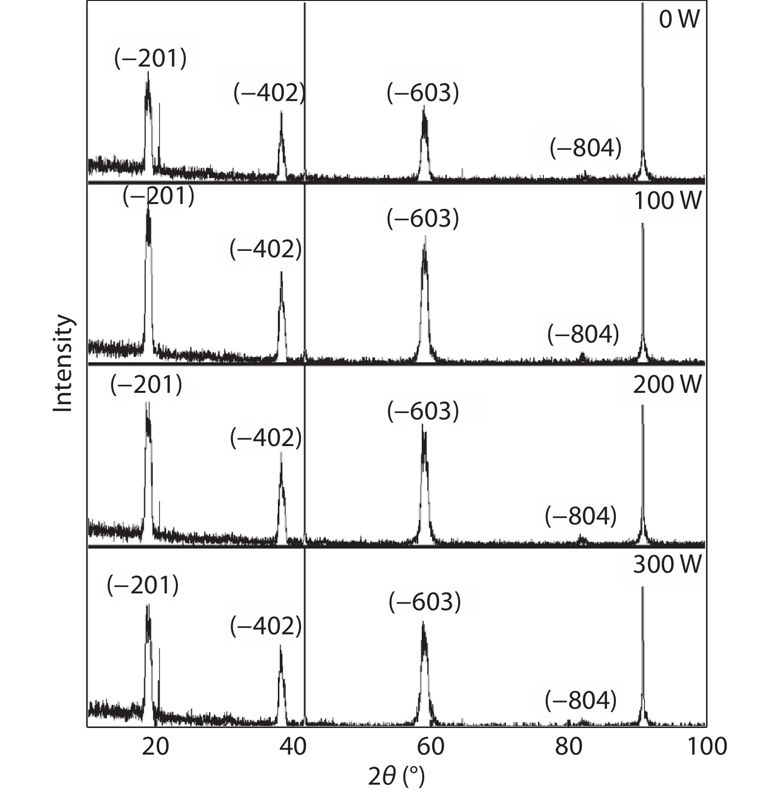
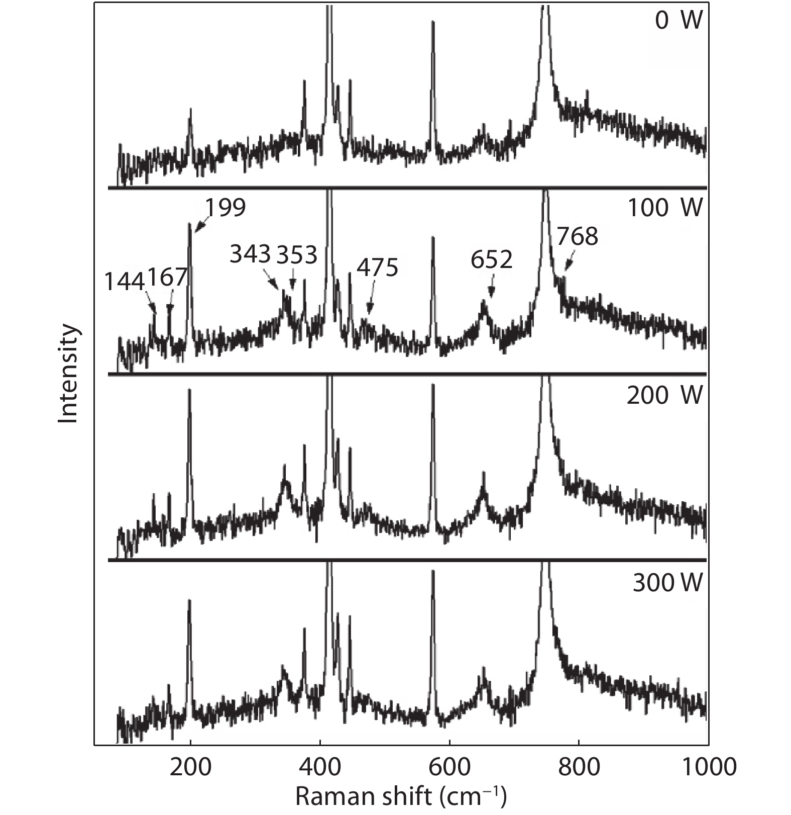
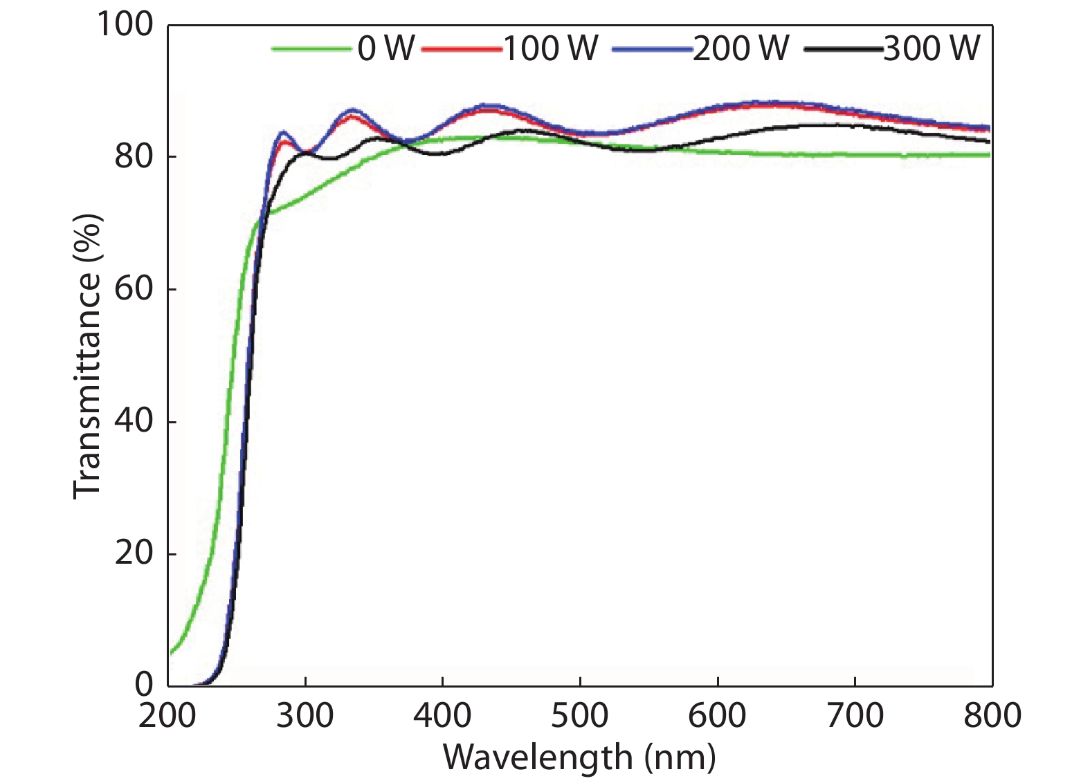
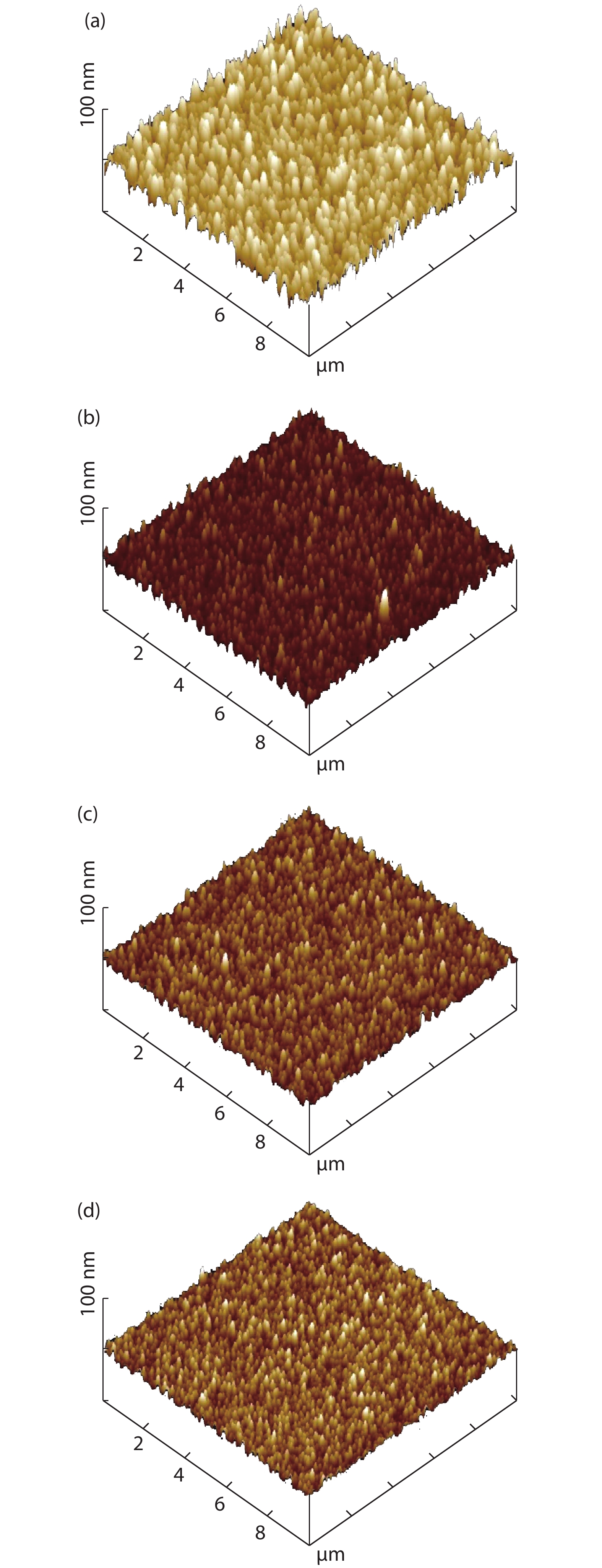
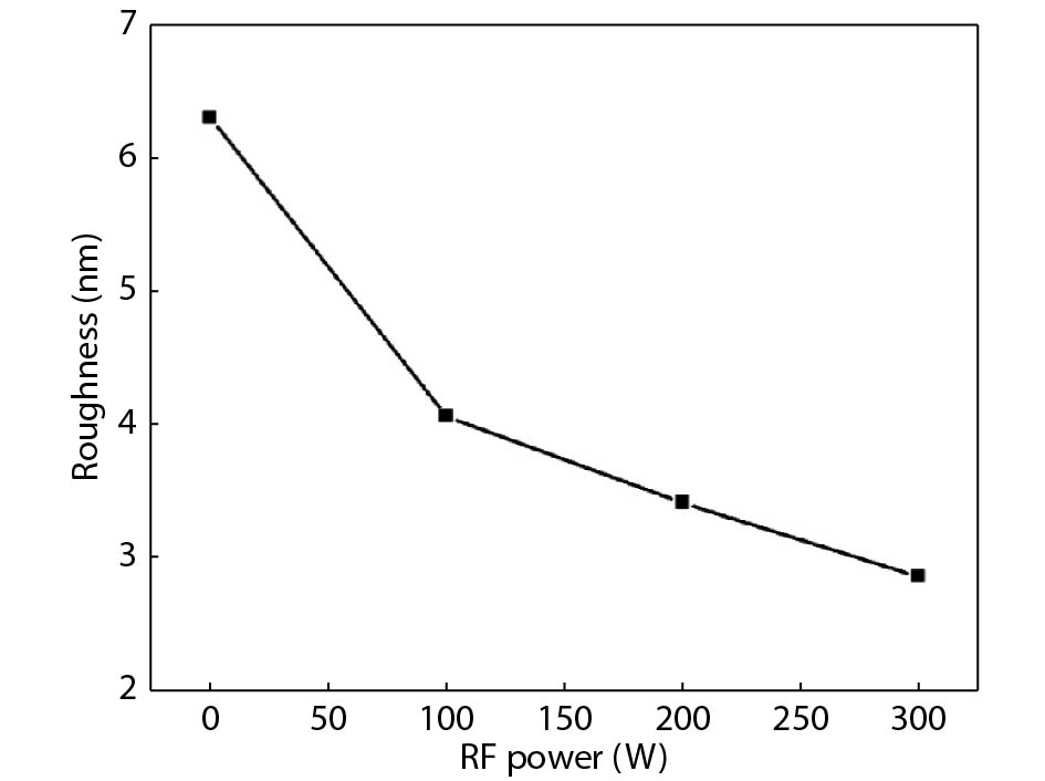
Table 1. Phonon modes for different samples compared with bulk β-Ga2O3.
| Peak location (cm?1) | Phonon mode | ||||
| 0 W | 100 W | 200 W | 300 W | Bulk | |
| – | 144 | 143.4 | 142.1 | 147 | Bg(2) |
| – | 167 | 167 | 166.4 | 169 | Ag(2) |
| 198.5 | 198.5 | 198.5 | 198.5 | 199 | Ag(3) |
| – | 348.3 | 345.2 | 344.6 | 346/353 | Ag(5)/Bg(3) |
| – | 470.7 | – | – | 475/475 | Ag(7)/Bg(4) |
| 652.6 | 652.6 | 652.6 | 652.6 | 651/657 | Bg(5)/Ag(9) |
| – | 767.8 | 768.4 | 763 | 763 | Ag(10) |
 DownLoad: CSV
| [1] |
Huang C Y, Horng R H, Wuu D S, et al. Thermal annealing effect on material characterizations of β-Ga2O3 epilayer grown by metal organic chemical vapor deposition. Appl Phys Lett, 2013, 102, 011119 doi: 10.1063/1.4773247
|
| [2] |
Roy R, Hill V G, Osborn E F. Polymorphism of Ga2O3 and the system Ga2O3–H2O. J Am Chem Soc, 1952, 74(3), 719 doi: 10.1021/ja01123a039
|
| [3] |
Binet L, Gourier D. Origin of the blue luminescence of β-Ga2O3. J Phys Chem Solids, 1998, 59(8), 1241 doi: 10.1016/S0022-3697(98)00047-X
|
| [4] |
Kokubun Y, Miura K, Endo F, et al. Sol-gel prepared β-Ga2O3 thin films for ultraviolet photodetectors. Appl Phys Lett, 2007, 90(3), 8 doi: 10.1063/1.2432946
|
| [5] |
Oshima T, Okuno T, Arai N, et al. Vertical solar-blind deep-ultraviolet schottky photodetectors based on β- Ga2O3substrates. Appl Phys Express, 2008, 1(1), 011202 doi: 10.1143/APEX.1.011202
|
| [6] |
Orita M, Ohta H, Hirano M, et al. Deep-ultraviolet transparent conductive β-Ga2O3 thin films. Appl Phys Lett, 2000, 77(25), 4166 doi: 10.1063/1.1330559
|
| [7] |
Orita M, Hiramatsu H, Ohta H, et al. Preparation of highly conductive, deep ultraviolet transparent β-Ga2O3 thin film at low deposition temperatures. Thin Solid Films, 2002, 411(1), 134 doi: 10.1016/S0040-6090(02)00202-X
|
| [8] |
Higashiwaki M, Sasaki K, Kamimura T, et al. Depletion-mode Ga2O3 metal-oxide-semiconductor field-effect transistors on β-Ga2O3 (010) substrates and temperature dependence of their device characteristics. Appl Phys Lett, 2013, 103(12), 123511 doi: 10.1063/1.4821858
|
| [9] |
Lee S A, Hwang J Y, Kim J P, et al. Dielectric characterization of transparent epitaxial Ga2O3 thin film on n-GaN∕Al2O3 prepared by pulsed laser deposition. Appl Phys Lett, 2006, 89(18), 182906 doi: 10.1063/1.2374806
|
| [10] |
Matsuzaki K, Yanagi H, Kamiya T, et al. Field-induced current modulation in epitaxial film of deep-ultraviolet transparent oxide semiconductor Ga2O3. Appl Phys Lett, 2006, 88(9), 092106 doi: 10.1063/1.2179373
|
| [11] |
Oshima T, Okuno T, Fujita S. Ga2O3 thin film growth on c-plane sapphire substrates by molecular beam epitaxy for deep-ultraviolet photodetectors. Jpn J Appl Phys, 2007, 46, 7217 doi: 10.1143/JJAP.46.7217
|
| [12] |
Oshima T, Arai N, Suzuki N, et al. Surface morphology of homoepitaxial β-Ga2O3 thin films grown by molecular beam epitaxy. Thin Solid Films, 2008, 516(17), 5768 doi: 10.1016/j.tsf.2007.10.045
|
| [13] |
Zhang F B, Saito K, Tanaka T, et al. Structural and optical properties of Ga2O3 films on sapphire substrates by pulsed laser deposition. J Cryst Growth, 2014, 387, 96 doi: 10.1016/j.jcrysgro.2013.11.022
|
| [14] |
Fleischer M, Hanrieder W, Meixner H. Stability of semiconducting gallium oxide thin films. Thin Solid Films, 1990, 190(1), 93 doi: 10.1016/0040-6090(90)90132-W
|
| [15] |
Liu J J, Yan J L, Shi L, et al. Electrical and optical properties of deep ultraviolet transparent conductive Ga2O3/ITO films by magnetron sputtering. J Semicond, 2010, 31(10), 103001 doi: 10.1088/1674-4926/31/10/103001
|
| [16] |
Shinohara D, Fujita S. Heteroepitaxy of corundum-structured α-Ga2O3 thin films on α-Al2O3 substrates by ultrasonic mist chemical vapor deposition. Jpn J Appl Phys, 2008, 47, 731 doi: 10.1143/JJAP.47.7311
|
| [17] |
Murakami H, Nomura K, Goto K, et al. Homoepitaxial growth of β-Ga2O3 layers by halide vapor phase epitaxy. Appl Phys Express, 2015, 8(1), 015503 doi: 10.7567/APEX.8.015503
|
| [18] |
Zhang F, Arita M, Wang X, et al. Toward controlling the carrier density of Si doped Ga2O3 films by pulsed laser deposition. Appl Phys Lett, 2016, 109(10), 102105 doi: 10.1063/1.4962463
|
| [19] |
Matsubara K, Fons P, Iwata K, et al. Room-temperature deposition of Al-doped ZnO films by oxygen radical-assisted pulsed laser deposition. Thin Solid Films, 2002, 422(1/2), 176 doi: 10.1016/S0040-6090(02)00965-3
|
| [20] |
Kakehi Y, Okamoto A, Sakurai Y, et al. Epitaxial growth of LiNbO3 thin films using pulsed laser deposition. Appl Surf Sci, 2001, 169/170(1/2), 560 doi: 10.1016/S0169-4332(00)00739-X
|
| [21] |
Oh M S, Hwang D K, Seong D J, et al. Improvement of characteristics of Ga-doped ZnO grown by pulsed laser deposition using plasma-enhanced oxygen radicals. J Electrochem Soc, 2008, 155(9), D599 doi: 10.1149/1.2952077
|
| [22] |
He X, Wu J, Zhao L, et al. Synthesis and optical properties of tantalum oxide films prepared by ionized plasma-assisted pulsed laser deposition. Solid State Commun, 2008, 147(3/4), 90 doi: 10.1016/j.ssc.2008.05.007
|
| [23] |
Madi C, Tabbal M, Christidis T, et al. Microstructural characterization of chromium oxide thin films grown by remote plasma assisted pulsed laser deposition. J Phys Conf Ser, 2007, 59(1), 600 doi: 10.1088/1742-6596/59/1/128
|
| [24] |
Wakabayashi R, Oshima T, Hattori M, et al. Oxygen-radical-assisted pulsed-laser deposition of β-Ga2O3 and β-(Al xGa1? x)2O3 films. J Cryst Growth, 2015, 424, 77 doi: 10.1016/j.jcrysgro.2015.05.005
|
| [25] |
Dohy D, Lucazeau G, Revcolevschi A. Raman spectra and valence force field of single-crystalline β Ga2O3. J Solid State Chem, 1982, 45(2), 180 doi: 10.1016/0022-4596(82)90274-2
|
| [26] |
Nagarajan L, De Souza R A, Samuelis D, et al. A chemically driven insulator-metal transition in non-stoichiometric and amorphous gallium oxide. Nat Mater, 2008, 7(5), 391 doi: 10.1038/nmat2164
|
| [27] |
Vogt P, Bierwagen O. Reaction kinetics and growth window for plasma-assisted molecular beam epitaxy of Ga2O3: Incorporation of Ga vs. Ga2O desorption. Appl Phys Lett, 2016, 108(7), 072101 doi: 10.1063/1.4942002
|
| [28] |
Vogt P, Bierwagen O. The competing oxide and sub-oxide formation in metal-oxide molecular beam epitaxy. Appl Phys Lett, 2015, 106(8), 081910 doi: 10.1063/1.4913447
|
| [29] |
Zhen Y, Ohsawa T, Adachi Y, et al. Investigations of growth kinetics of pulsed laser deposition of tin oxide films by isotope tracer technique. J Appl Phys, 2010, 108(10), 104901 doi: 10.1063/1.3506714
|
| [30] |
Matsumoto K, Adachi Y, Sakaguchi I, et al. Preparation and characterization of Zn18O/Zn16O isotope heterostructure thin films. J Eur Ceram Soc, 2010, 30(2), 423 doi: 10.1016/j.jeurceramsoc.2009.06.023
|


Article views: 5788 Times PDF downloads: 124 Times Cited by: 0 Times
Received: 30 July 2018 Revised: 02 October 2018 Online: Accepted Manuscript: 08 January 2019Uncorrected proof: 09 January 2019Published: 09 December 2019
| Citation: |
Congyu Hu, Katsuhiko Saito, Tooru Tanaka, Qixin Guo. Growth properties of gallium oxide on sapphire substrate by plasma-assisted pulsed laser deposition[J]. Journal of Semiconductors, 2019, 40(12): 122801. doi: 10.1088/1674-4926/40/12/122801
****
C Y Hu, K Saito, T Tanaka, Q X Guo, Growth properties of gallium oxide on sapphire substrate by plasma-assisted pulsed laser deposition[J]. J. Semicond., 2019, 40(12): 122801. doi: 10.1088/1674-4926/40/12/122801.

|
| [1] |
Huang C Y, Horng R H, Wuu D S, et al. Thermal annealing effect on material characterizations of β-Ga2O3 epilayer grown by metal organic chemical vapor deposition. Appl Phys Lett, 2013, 102, 011119 doi: 10.1063/1.4773247
|
| [2] |
Roy R, Hill V G, Osborn E F. Polymorphism of Ga2O3 and the system Ga2O3–H2O. J Am Chem Soc, 1952, 74(3), 719 doi: 10.1021/ja01123a039
|
| [3] |
Binet L, Gourier D. Origin of the blue luminescence of β-Ga2O3. J Phys Chem Solids, 1998, 59(8), 1241 doi: 10.1016/S0022-3697(98)00047-X
|
| [4] |
Kokubun Y, Miura K, Endo F, et al. Sol-gel prepared β-Ga2O3 thin films for ultraviolet photodetectors. Appl Phys Lett, 2007, 90(3), 8 doi: 10.1063/1.2432946
|
| [5] |
Oshima T, Okuno T, Arai N, et al. Vertical solar-blind deep-ultraviolet schottky photodetectors based on β- Ga2O3substrates. Appl Phys Express, 2008, 1(1), 011202 doi: 10.1143/APEX.1.011202
|
| [6] |
Orita M, Ohta H, Hirano M, et al. Deep-ultraviolet transparent conductive β-Ga2O3 thin films. Appl Phys Lett, 2000, 77(25), 4166 doi: 10.1063/1.1330559
|
| [7] |
Orita M, Hiramatsu H, Ohta H, et al. Preparation of highly conductive, deep ultraviolet transparent β-Ga2O3 thin film at low deposition temperatures. Thin Solid Films, 2002, 411(1), 134 doi: 10.1016/S0040-6090(02)00202-X
|
| [8] |
Higashiwaki M, Sasaki K, Kamimura T, et al. Depletion-mode Ga2O3 metal-oxide-semiconductor field-effect transistors on β-Ga2O3 (010) substrates and temperature dependence of their device characteristics. Appl Phys Lett, 2013, 103(12), 123511 doi: 10.1063/1.4821858
|
| [9] |
Lee S A, Hwang J Y, Kim J P, et al. Dielectric characterization of transparent epitaxial Ga2O3 thin film on n-GaN∕Al2O3 prepared by pulsed laser deposition. Appl Phys Lett, 2006, 89(18), 182906 doi: 10.1063/1.2374806
|
| [10] |
Matsuzaki K, Yanagi H, Kamiya T, et al. Field-induced current modulation in epitaxial film of deep-ultraviolet transparent oxide semiconductor Ga2O3. Appl Phys Lett, 2006, 88(9), 092106 doi: 10.1063/1.2179373
|
| [11] |
Oshima T, Okuno T, Fujita S. Ga2O3 thin film growth on c-plane sapphire substrates by molecular beam epitaxy for deep-ultraviolet photodetectors. Jpn J Appl Phys, 2007, 46, 7217 doi: 10.1143/JJAP.46.7217
|
| [12] |
Oshima T, Arai N, Suzuki N, et al. Surface morphology of homoepitaxial β-Ga2O3 thin films grown by molecular beam epitaxy. Thin Solid Films, 2008, 516(17), 5768 doi: 10.1016/j.tsf.2007.10.045
|
| [13] |
Zhang F B, Saito K, Tanaka T, et al. Structural and optical properties of Ga2O3 films on sapphire substrates by pulsed laser deposition. J Cryst Growth, 2014, 387, 96 doi: 10.1016/j.jcrysgro.2013.11.022
|
| [14] |
Fleischer M, Hanrieder W, Meixner H. Stability of semiconducting gallium oxide thin films. Thin Solid Films, 1990, 190(1), 93 doi: 10.1016/0040-6090(90)90132-W
|
| [15] |
Liu J J, Yan J L, Shi L, et al. Electrical and optical properties of deep ultraviolet transparent conductive Ga2O3/ITO films by magnetron sputtering. J Semicond, 2010, 31(10), 103001 doi: 10.1088/1674-4926/31/10/103001
|
| [16] |
Shinohara D, Fujita S. Heteroepitaxy of corundum-structured α-Ga2O3 thin films on α-Al2O3 substrates by ultrasonic mist chemical vapor deposition. Jpn J Appl Phys, 2008, 47, 731 doi: 10.1143/JJAP.47.7311
|
| [17] |
Murakami H, Nomura K, Goto K, et al. Homoepitaxial growth of β-Ga2O3 layers by halide vapor phase epitaxy. Appl Phys Express, 2015, 8(1), 015503 doi: 10.7567/APEX.8.015503
|
| [18] |
Zhang F, Arita M, Wang X, et al. Toward controlling the carrier density of Si doped Ga2O3 films by pulsed laser deposition. Appl Phys Lett, 2016, 109(10), 102105 doi: 10.1063/1.4962463
|
| [19] |
Matsubara K, Fons P, Iwata K, et al. Room-temperature deposition of Al-doped ZnO films by oxygen radical-assisted pulsed laser deposition. Thin Solid Films, 2002, 422(1/2), 176 doi: 10.1016/S0040-6090(02)00965-3
|
| [20] |
Kakehi Y, Okamoto A, Sakurai Y, et al. Epitaxial growth of LiNbO3 thin films using pulsed laser deposition. Appl Surf Sci, 2001, 169/170(1/2), 560 doi: 10.1016/S0169-4332(00)00739-X
|
| [21] |
Oh M S, Hwang D K, Seong D J, et al. Improvement of characteristics of Ga-doped ZnO grown by pulsed laser deposition using plasma-enhanced oxygen radicals. J Electrochem Soc, 2008, 155(9), D599 doi: 10.1149/1.2952077
|
| [22] |
He X, Wu J, Zhao L, et al. Synthesis and optical properties of tantalum oxide films prepared by ionized plasma-assisted pulsed laser deposition. Solid State Commun, 2008, 147(3/4), 90 doi: 10.1016/j.ssc.2008.05.007
|
| [23] |
Madi C, Tabbal M, Christidis T, et al. Microstructural characterization of chromium oxide thin films grown by remote plasma assisted pulsed laser deposition. J Phys Conf Ser, 2007, 59(1), 600 doi: 10.1088/1742-6596/59/1/128
|
| [24] |
Wakabayashi R, Oshima T, Hattori M, et al. Oxygen-radical-assisted pulsed-laser deposition of β-Ga2O3 and β-(Al xGa1? x)2O3 films. J Cryst Growth, 2015, 424, 77 doi: 10.1016/j.jcrysgro.2015.05.005
|
| [25] |
Dohy D, Lucazeau G, Revcolevschi A. Raman spectra and valence force field of single-crystalline β Ga2O3. J Solid State Chem, 1982, 45(2), 180 doi: 10.1016/0022-4596(82)90274-2
|
| [26] |
Nagarajan L, De Souza R A, Samuelis D, et al. A chemically driven insulator-metal transition in non-stoichiometric and amorphous gallium oxide. Nat Mater, 2008, 7(5), 391 doi: 10.1038/nmat2164
|
| [27] |
Vogt P, Bierwagen O. Reaction kinetics and growth window for plasma-assisted molecular beam epitaxy of Ga2O3: Incorporation of Ga vs. Ga2O desorption. Appl Phys Lett, 2016, 108(7), 072101 doi: 10.1063/1.4942002
|
| [28] |
Vogt P, Bierwagen O. The competing oxide and sub-oxide formation in metal-oxide molecular beam epitaxy. Appl Phys Lett, 2015, 106(8), 081910 doi: 10.1063/1.4913447
|
| [29] |
Zhen Y, Ohsawa T, Adachi Y, et al. Investigations of growth kinetics of pulsed laser deposition of tin oxide films by isotope tracer technique. J Appl Phys, 2010, 108(10), 104901 doi: 10.1063/1.3506714
|
| [30] |
Matsumoto K, Adachi Y, Sakaguchi I, et al. Preparation and characterization of Zn18O/Zn16O isotope heterostructure thin films. J Eur Ceram Soc, 2010, 30(2), 423 doi: 10.1016/j.jeurceramsoc.2009.06.023
|

 WeChat ID
Journal of Semiconductors © 2017 All Rights Reserved 京ICP備05085259號(hào)-2

