


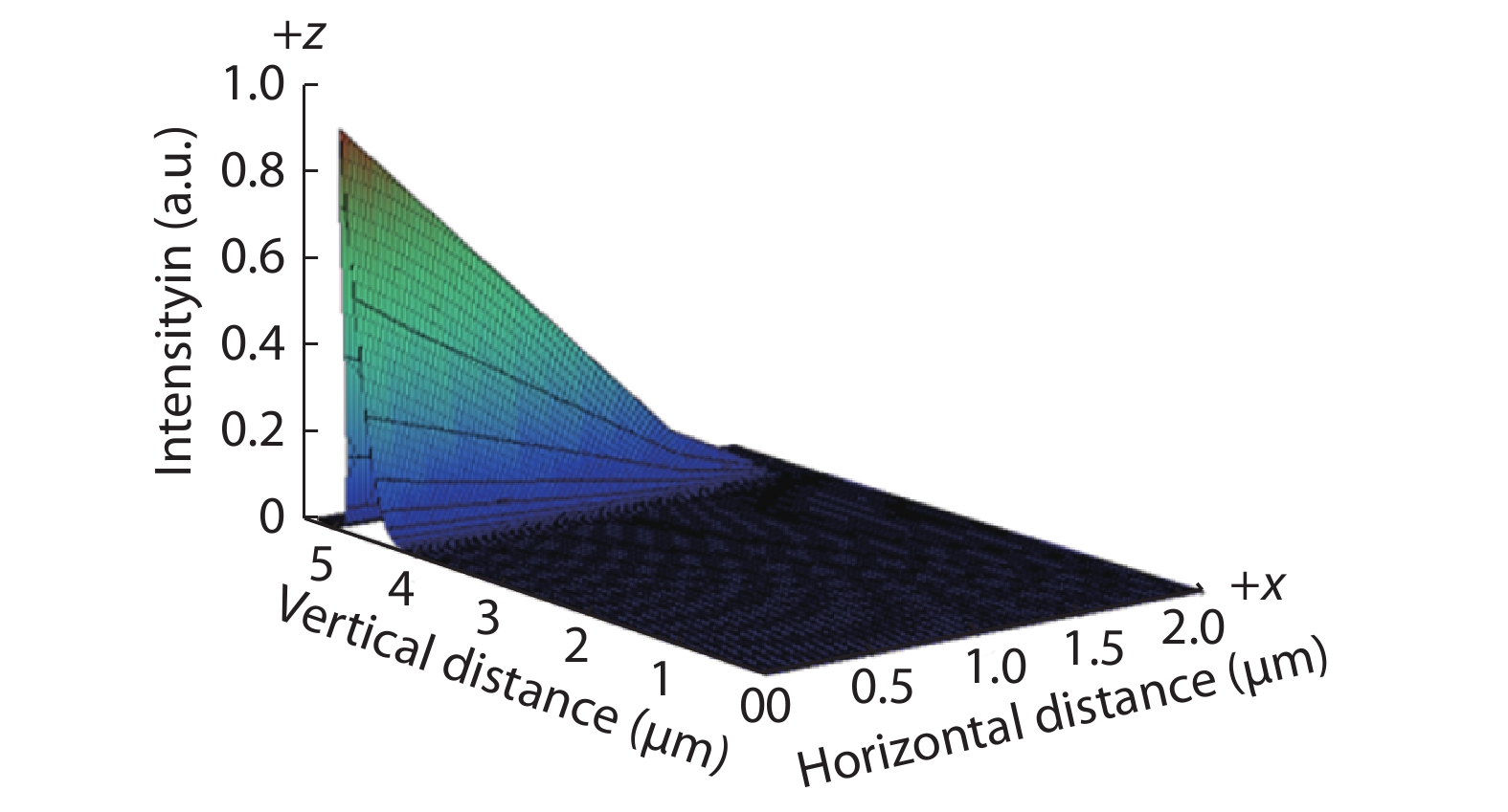
Fig. 1.
(Color online) The optical intensity confined within the active region for optical confining factor (OCF) of 40.4%.
ARTICLES
Mussaab I. Niass1, 2, 3, , Muhammad Nawaz Sharif1, 2, 3, Yifu Wang1, 2, 3, Zhengqian Lu1, 2, 3, Xue Chen1, 2, 3, Yipu Qu1, 2, 3, Zhongqiu Du1, 2, 3, Fang Wang1, 2, 3, and Yuhuai Liu1, 2, 3,
Corresponding author: Mussaab I. Niass, mussaab99@gmail.com, iefwang@zzu.edu.cn, ieyhliu@zzu.edu.cn; Fang Wang, mussaab99@gmail.com, iefwang@zzu.edu.cn, ieyhliu@zzu.edu.cn; Yuhuai Liu, mussaab99@gmail.com, iefwang@zzu.edu.cn, ieyhliu@zzu.edu.cn
Abstract: In this paper, an ultraviolet C-band laser diode lasing at 277 nm composed of B0.313Ga0.687N/B0.40Ga0.60N QW/QB heterostructure on Mg and Si-doped AlxGa1–xN layers was designed, as well as a lowest reported substitutional accepter and donor concentration up to NA = 5.0 × 1017 cm–3 and ND = 9.0 × 1016 cm–3 for deep ultraviolet lasing was achieved. The structure was assumed to be grown over bulk AlN substrate and operate under a continuous wave at room temperature. Although there is an emphasizing of the suitability for using boron nitride wide band gap in the deep ultraviolet region, there is still a shortage of investigation about the ternary BGaN in aluminum-rich AlGaN alloys. Based on the simulation, an average local gain in quantum wells of 1946 cm–1, the maximum emitted power of 2.4 W, the threshold current of 500 mA, a slope efficiency of 1.91 W/A as well as an average DC resistance for the V–I curve of (0.336 Ω) had been observed. Along with an investigation regarding different EBL, designs were included with tapered and inverse tapered structure. Therefore, it had been found a good agreement with the published results for tapered EBL design, with an overweighting for a proposed inverse tapered EBL design.
Key words: laser diodes, semiconducting aluminum compounds, heterojunction semiconductor devices, quantum wells, semiconducting ternary compounds
| [1] |
Li D B, Sun X J, Guo C L. AlGaN photonics: recent advances in materials and ultraviolet devices. Adv Opt Photon, 2018, 10, 43 doi: 10.1364/AOP.10.000043
|
| [2] |
Chowdhury M Z, Hossan M T, Islam A, et al. A comparative survey of optical wireless technologies: architectures and applications. IEEE Access, 2018, 6, 9819 doi: 10.1109/ACCESS.2018.2792419
|
| [3] |
Chen J R, Ko T S, Su P Y, et al. Numerical study on optimization of active layer structures for GaN/AlGaN multiple-quantum-well laser diodes. J Lightwave Technol, 2008, 26, 3155 doi: 10.1109/JLT.2008.926939
|
| [4] |
Watanabe T, Niiyama T, Miya K, et al. Far-ultraviolet plane-emission handheld device based on hexagonal boron nitride. Nat Photonics, 2009, 3, 591 doi: 10.1038/nphoton.2009.167
|
| [5] |
Watanabe K, Taniguchi T. Hexagonal boron nitride as a new ultraviolet luminescent material and its application. Int J Appl Ceram Technol, 2011, 8, 977 doi: 10.1111/j.1744-7402.2011.02626.x
|
| [6] |
Kawanishi H, Haruyama M, Shirai T, et al. (BAlGa)N quaternary system and epitaxial growth on (0001) 6H-SiC substrate by low-pressure MO-VPE. Proc SPIE, 1997, 2994, 52 doi: 10.1117/12.275585
|
| [7] |
Kurimoto M, Takano T, Yamamoto J, et al. Growth of BGaN/AlGaN multi-quantum-well structure by metalorganic vapor phase epitaxy. J Cryst Growth, 2000, 221, 378 doi: 10.1016/S0022-0248(00)00717-X
|
| [8] |
Honda T, Kurimoto M, Shibata M, et al. Excitonic emission of BGaN grown on (0 0 0 1) 6H-SiC by metal-organic vapor-phase epitaxy. J Lumin, 2000, 87–89, 1274 doi: 10.1016/S0022-2313(99)00565-7
|
| [9] |
Dahal J L R, Majety S, Pantha B N, et al. Epitaxially grown semiconducting hexagonal boron nitride as a deep ultraviolet photonic materia. Appl Phys Lett, 2011, 98, 211110 doi: 10.1063/1.3593958
|
| [10] |
Majety J L S, Cao X K, Dahal R, et al. Epitaxial growth and demonstration of hexagonal BN/AlGaN p–n junctions for deep ultraviolet photonics. Appl Phys Lett, 2012, 100, 061121 doi: 10.1063/1.3682523
|
| [11] |
Jiang H X, Lin J Y. Hexagonal boron nitride for deep ultraviolet photonic devices. Semicond Sci Technol, 2014, 29, 1 doi: 10.1088/0268-1242/29/8/084003
|
| [12] |
Satter M M, Kim H J, Lochner Z, et al. Design and analysis of 250-nm AlInN laser diodes on AlN substrates using tapered electron blocking layers. IEEE J Quantum Electron, 2012, 48, 703 doi: 10.1109/JQE.2012.2190496
|
| [13] |
Sailo L, Ralte R L, Lalchhuanawmi M, et al. Calculation of the band structure and band splitting energy of boron compounds (BX, X = N, P, As, Sb) using modified Becke-Johnson potential. IOSR-JAP, 2016, 8, 1
|
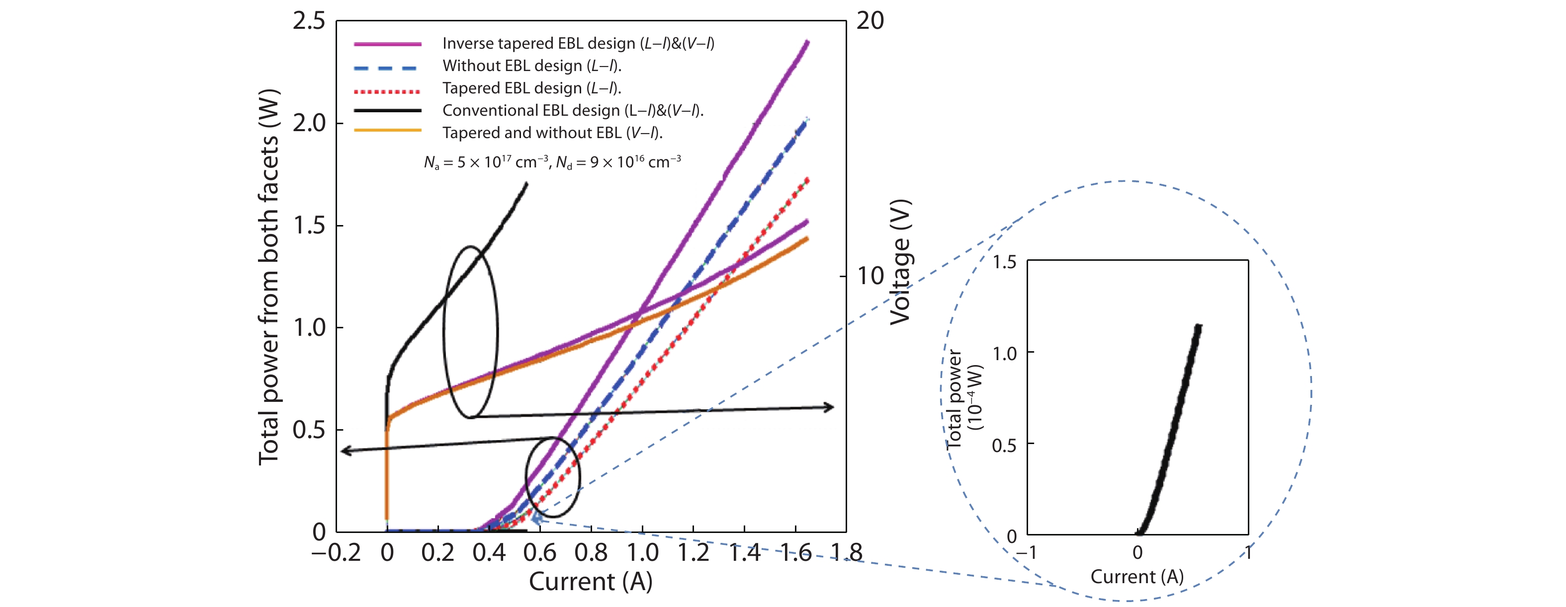
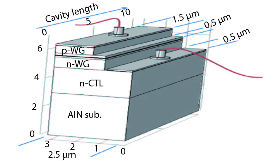
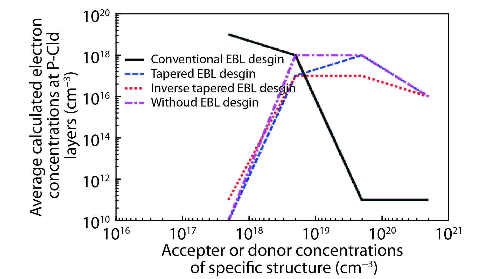
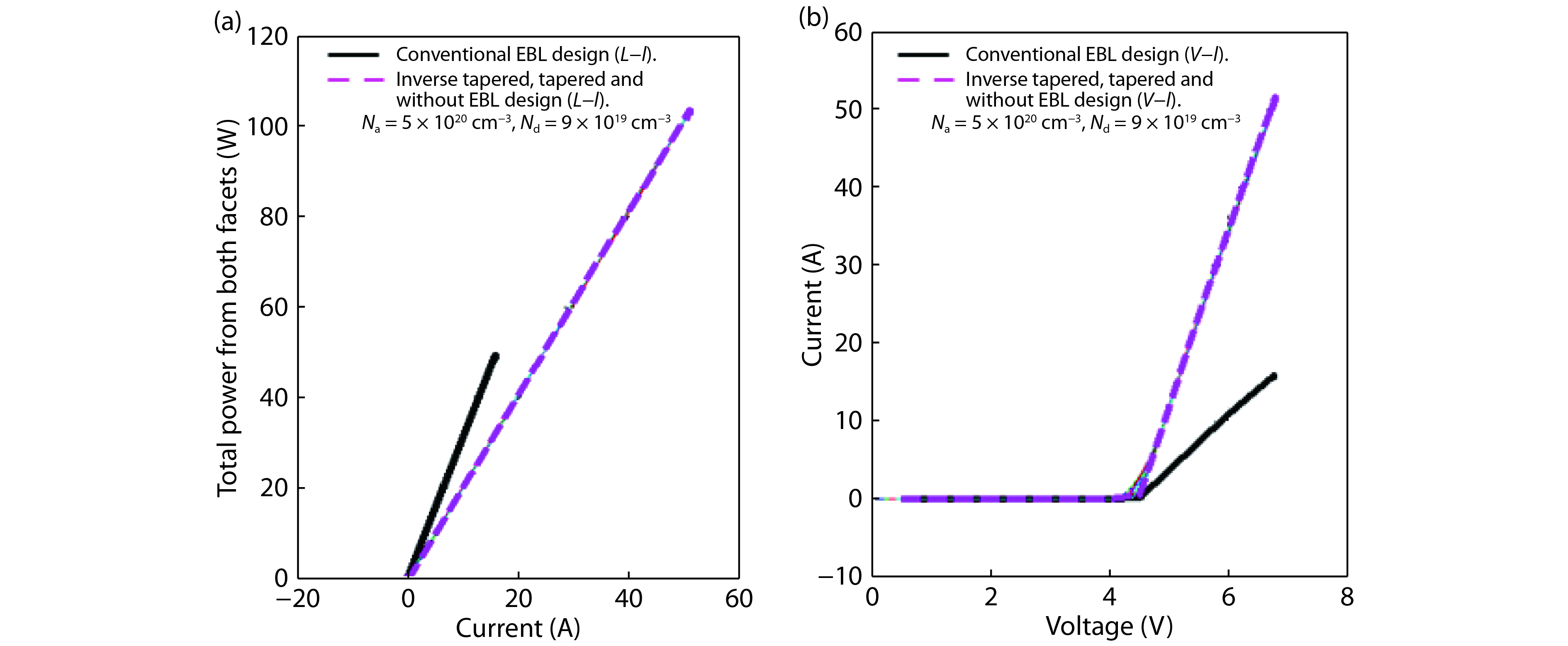
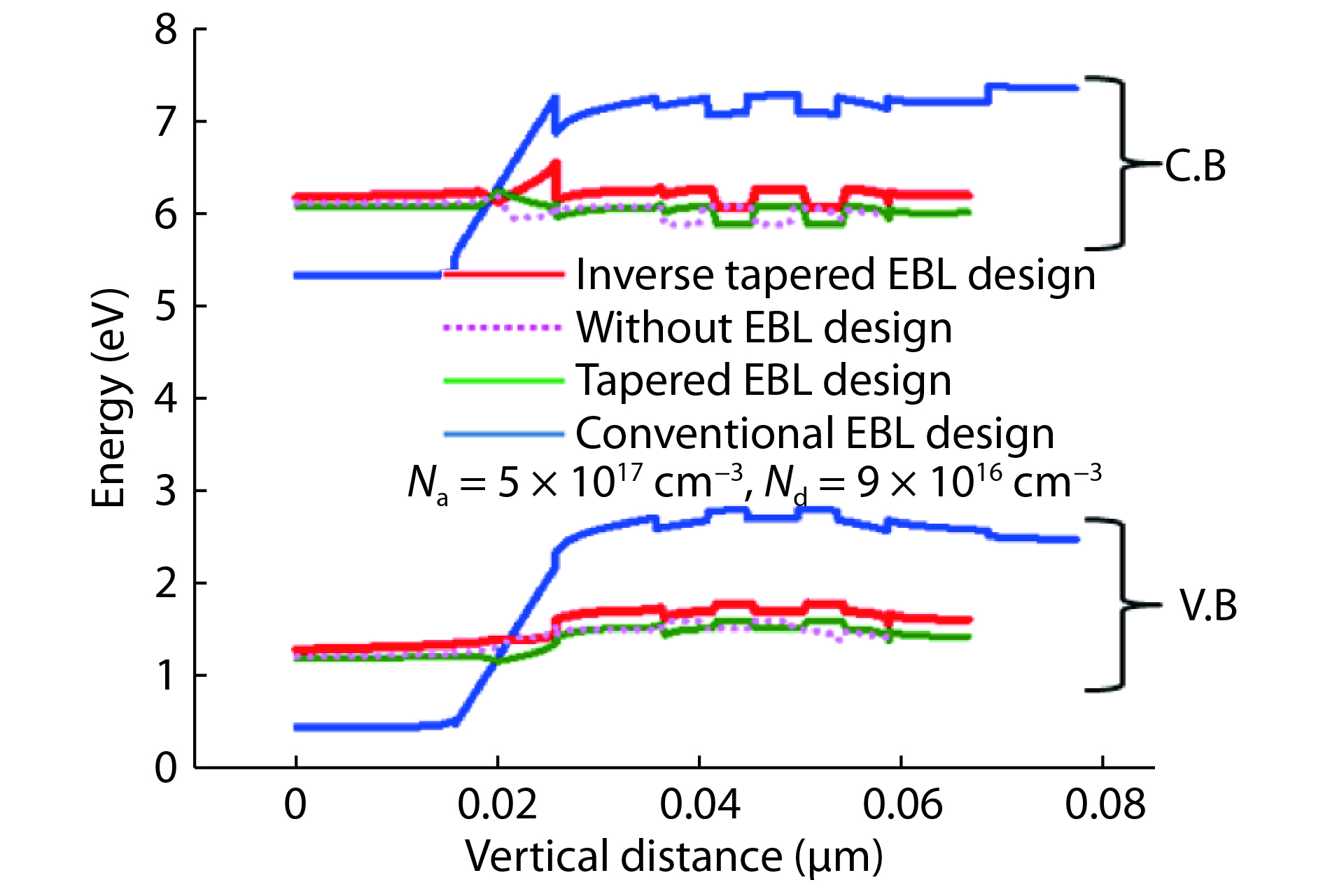
Table 1. The contrived LD structure at room temperature for B0.313GaN/B0.40GaN MQW (p, p-type Mg-dopant; n, n-type Si-dopant; i, intrinsic/no-doping; CLL, cladding layer; WG, wave guide; EBL-IT, electron blocking layer-inverse tapered).
| Layer material | Layer function | Thickness (nm) | Real refractive index |
| p-Al0.87GaN | p-WG | 500 | 2.20 |
| p-Al0.71–0.77GaN | p-CLL | 150 | 2.263–2.239 |
| i-Al0.80–0.65GaN | EBL-IT | 10 | 2.228–2.286 |
| p-Al0.57GaN | Spacer-1 | 10 | 2.317 |
| i-B0.40GaN × (3) | QB | 5 | 2.343 |
| i-B0.313GaN × (2) | QW | 4 | 2.286 |
| n-Al0.61–0.58GaN | Spacer-2 | 10 | 2.30–2.313 |
| n-Al0.77–0.71GaN | n-CLL | 100 | 2.24–2.63 |
| n-Al0.77GaN | n-WG-1 | 685 | 2.24 |
| n-Al0.77GaN | n-WG-2 | 1800 | 2.24 |
| i-AlN | Substrate | 2000 | 2.15 |
 DownLoad: CSV
| [1] |
Li D B, Sun X J, Guo C L. AlGaN photonics: recent advances in materials and ultraviolet devices. Adv Opt Photon, 2018, 10, 43 doi: 10.1364/AOP.10.000043
|
| [2] |
Chowdhury M Z, Hossan M T, Islam A, et al. A comparative survey of optical wireless technologies: architectures and applications. IEEE Access, 2018, 6, 9819 doi: 10.1109/ACCESS.2018.2792419
|
| [3] |
Chen J R, Ko T S, Su P Y, et al. Numerical study on optimization of active layer structures for GaN/AlGaN multiple-quantum-well laser diodes. J Lightwave Technol, 2008, 26, 3155 doi: 10.1109/JLT.2008.926939
|
| [4] |
Watanabe T, Niiyama T, Miya K, et al. Far-ultraviolet plane-emission handheld device based on hexagonal boron nitride. Nat Photonics, 2009, 3, 591 doi: 10.1038/nphoton.2009.167
|
| [5] |
Watanabe K, Taniguchi T. Hexagonal boron nitride as a new ultraviolet luminescent material and its application. Int J Appl Ceram Technol, 2011, 8, 977 doi: 10.1111/j.1744-7402.2011.02626.x
|
| [6] |
Kawanishi H, Haruyama M, Shirai T, et al. (BAlGa)N quaternary system and epitaxial growth on (0001) 6H-SiC substrate by low-pressure MO-VPE. Proc SPIE, 1997, 2994, 52 doi: 10.1117/12.275585
|
| [7] |
Kurimoto M, Takano T, Yamamoto J, et al. Growth of BGaN/AlGaN multi-quantum-well structure by metalorganic vapor phase epitaxy. J Cryst Growth, 2000, 221, 378 doi: 10.1016/S0022-0248(00)00717-X
|
| [8] |
Honda T, Kurimoto M, Shibata M, et al. Excitonic emission of BGaN grown on (0 0 0 1) 6H-SiC by metal-organic vapor-phase epitaxy. J Lumin, 2000, 87–89, 1274 doi: 10.1016/S0022-2313(99)00565-7
|
| [9] |
Dahal J L R, Majety S, Pantha B N, et al. Epitaxially grown semiconducting hexagonal boron nitride as a deep ultraviolet photonic materia. Appl Phys Lett, 2011, 98, 211110 doi: 10.1063/1.3593958
|
| [10] |
Majety J L S, Cao X K, Dahal R, et al. Epitaxial growth and demonstration of hexagonal BN/AlGaN p–n junctions for deep ultraviolet photonics. Appl Phys Lett, 2012, 100, 061121 doi: 10.1063/1.3682523
|
| [11] |
Jiang H X, Lin J Y. Hexagonal boron nitride for deep ultraviolet photonic devices. Semicond Sci Technol, 2014, 29, 1 doi: 10.1088/0268-1242/29/8/084003
|
| [12] |
Satter M M, Kim H J, Lochner Z, et al. Design and analysis of 250-nm AlInN laser diodes on AlN substrates using tapered electron blocking layers. IEEE J Quantum Electron, 2012, 48, 703 doi: 10.1109/JQE.2012.2190496
|
| [13] |
Sailo L, Ralte R L, Lalchhuanawmi M, et al. Calculation of the band structure and band splitting energy of boron compounds (BX, X = N, P, As, Sb) using modified Becke-Johnson potential. IOSR-JAP, 2016, 8, 1
|


Article views: 4915 Times PDF downloads: 72 Times Cited by: 0 Times
Received: 26 December 2018 Revised: 30 April 2019 Online: Accepted Manuscript: 28 May 2019Uncorrected proof: 29 May 2019Published: 09 December 2019
| Citation: |
Mussaab I. Niass, Muhammad Nawaz Sharif, Yifu Wang, Zhengqian Lu, Xue Chen, Yipu Qu, Zhongqiu Du, Fang Wang, Yuhuai Liu. A contrivance of 277 nm DUV LD with B0.313Ga0.687N/B0.40Ga0.60N QWs and AlxGa1–xN heterojunction grown on AlN substrate[J]. Journal of Semiconductors, 2019, 40(12): 122802. doi: 10.1088/1674-4926/40/12/122802
****
M I Niass, M N Sharif, Y F Wang, Z Q Lu, X Chen, Y P Qu, Z Q Du, F Wang, Y H Liu, A contrivance of 277 nm DUV LD with B0.313Ga0.687N/B0.40Ga0.60N QWs and AlxGa1–xN heterojunction grown on AlN substrate[J]. J. Semicond., 2019, 40(12): 122802. doi: 10.1088/1674-4926/40/12/122802.

|
| [1] |
Li D B, Sun X J, Guo C L. AlGaN photonics: recent advances in materials and ultraviolet devices. Adv Opt Photon, 2018, 10, 43 doi: 10.1364/AOP.10.000043
|
| [2] |
Chowdhury M Z, Hossan M T, Islam A, et al. A comparative survey of optical wireless technologies: architectures and applications. IEEE Access, 2018, 6, 9819 doi: 10.1109/ACCESS.2018.2792419
|
| [3] |
Chen J R, Ko T S, Su P Y, et al. Numerical study on optimization of active layer structures for GaN/AlGaN multiple-quantum-well laser diodes. J Lightwave Technol, 2008, 26, 3155 doi: 10.1109/JLT.2008.926939
|
| [4] |
Watanabe T, Niiyama T, Miya K, et al. Far-ultraviolet plane-emission handheld device based on hexagonal boron nitride. Nat Photonics, 2009, 3, 591 doi: 10.1038/nphoton.2009.167
|
| [5] |
Watanabe K, Taniguchi T. Hexagonal boron nitride as a new ultraviolet luminescent material and its application. Int J Appl Ceram Technol, 2011, 8, 977 doi: 10.1111/j.1744-7402.2011.02626.x
|
| [6] |
Kawanishi H, Haruyama M, Shirai T, et al. (BAlGa)N quaternary system and epitaxial growth on (0001) 6H-SiC substrate by low-pressure MO-VPE. Proc SPIE, 1997, 2994, 52 doi: 10.1117/12.275585
|
| [7] |
Kurimoto M, Takano T, Yamamoto J, et al. Growth of BGaN/AlGaN multi-quantum-well structure by metalorganic vapor phase epitaxy. J Cryst Growth, 2000, 221, 378 doi: 10.1016/S0022-0248(00)00717-X
|
| [8] |
Honda T, Kurimoto M, Shibata M, et al. Excitonic emission of BGaN grown on (0 0 0 1) 6H-SiC by metal-organic vapor-phase epitaxy. J Lumin, 2000, 87–89, 1274 doi: 10.1016/S0022-2313(99)00565-7
|
| [9] |
Dahal J L R, Majety S, Pantha B N, et al. Epitaxially grown semiconducting hexagonal boron nitride as a deep ultraviolet photonic materia. Appl Phys Lett, 2011, 98, 211110 doi: 10.1063/1.3593958
|
| [10] |
Majety J L S, Cao X K, Dahal R, et al. Epitaxial growth and demonstration of hexagonal BN/AlGaN p–n junctions for deep ultraviolet photonics. Appl Phys Lett, 2012, 100, 061121 doi: 10.1063/1.3682523
|
| [11] |
Jiang H X, Lin J Y. Hexagonal boron nitride for deep ultraviolet photonic devices. Semicond Sci Technol, 2014, 29, 1 doi: 10.1088/0268-1242/29/8/084003
|
| [12] |
Satter M M, Kim H J, Lochner Z, et al. Design and analysis of 250-nm AlInN laser diodes on AlN substrates using tapered electron blocking layers. IEEE J Quantum Electron, 2012, 48, 703 doi: 10.1109/JQE.2012.2190496
|
| [13] |
Sailo L, Ralte R L, Lalchhuanawmi M, et al. Calculation of the band structure and band splitting energy of boron compounds (BX, X = N, P, As, Sb) using modified Becke-Johnson potential. IOSR-JAP, 2016, 8, 1
|

 WeChat ID
Journal of Semiconductors © 2017 All Rights Reserved 京ICP備05085259號-2

