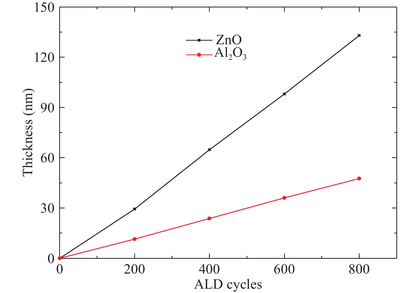
Fig. 1.
(Color online) Thicknesses of ZnO and Al2O3 films as a function of ALD cycle.
SEMICONDUCTOR MATERIALS
Li Chen1, 2, 3, Xinliang Chen1, 2, 3, , Zhongxin Zhou1, 2, 3, Sheng Guo1, 2, 3, Ying Zhao1, 2, 3 and Xiaodan Zhang1, 2, 3
Corresponding author: Xinliang Chen, E-mail: cxlruzhou@163.com
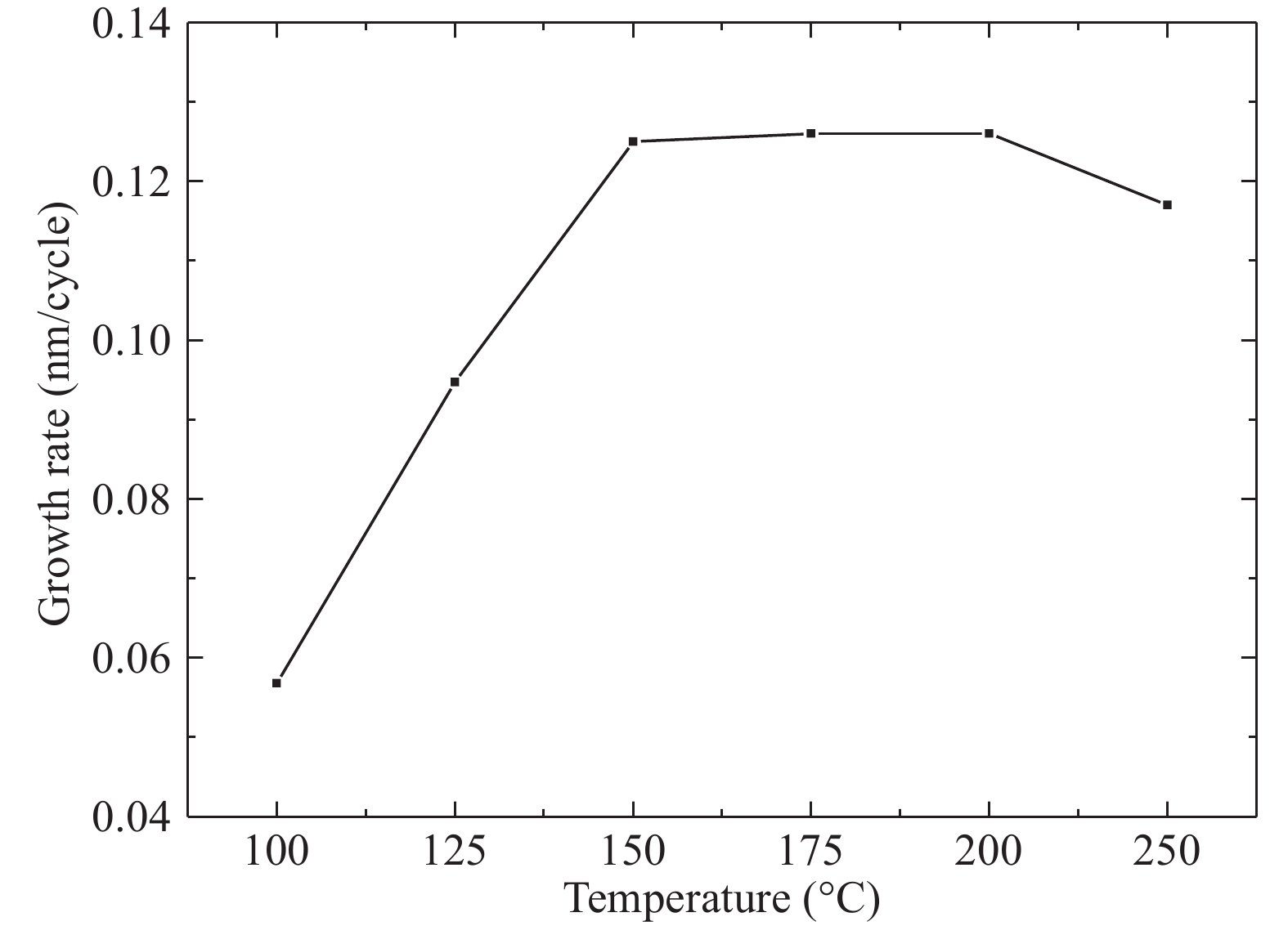
Abstract: Al doped ZnO (AZO) films deposited on glass substrates through the atomic layer deposition (ALD) technique are investigated with various temperatures from 100 to 250 °C and different Zn : Al cycle ratios from 20 : 0 to 20 : 3. Surface morphology, structure, optical and electrical properties of obtained AZO films are studied in detail. The Al composition of the AZO films is varied by controlling the ratio of Zn : Al. We achieve an excellent AZO thin film with a resistivity of 2.14 × 10?3 Ω·cm and high optical transmittance deposited at 150 °C with 20 : 2 Zn : Al cycle ratio. This kind of AZO thin films exhibit great potential for optoelectronics device application.
Key words: AZO films, ALD, Zn : Al cycle ratio, optical and electrical properties
| [1] |
Kim H, Gilmore C M, Gilmore J S, et al. Transparent conducting aluminum-doped zinc oxide thin films for organic light-emitting devices. Appl Phys Lett, 2000, 76: 259 doi: 10.1063/1.125740
|
| [2] |
Nomura K, Ohta H, Takagi A, et al. Room-temperature fabrication of transparent flexible thin-film transistors using amorphous oxide semiconductors. Nature, 2004, 432: 488 doi: 10.1038/nature03090
|
| [3] |
Minami T. Transparent conducting oxide semiconductors for transparent electrodes. Semicond Sci Technol, 2005, 20: 35 doi: 10.1088/0268-1242/20/4/004
|
| [4] |
Du X, George S M. Thickness dependence of sensor response for CO gas sensing by tin oxide films grown using atomic layer deposition. Sens Actuator B, 2008, 135: 152 doi: 10.1016/j.snb.2008.08.015
|
| [5] |
Martinson A B F, Elam J W, Hupp J T, et al. ZnO nanotube based dye-sensitized solar cells. Nano Lett, 2007, 7: 2183 doi: 10.1021/nl070160+
|
| [6] |
Meyer J, Gorrn P, Hamwi S, et al. Indium-free transparent organic light emitting diodes with Al doped ZnO electrodes grown by atomic layer and pulsed laser deposition. Appl Phys Lett, 2008, 93: 073308 doi: 10.1063/1.2975176
|
| [7] |
Lim J, Lee C. Effects of substrate temperature on the microstructure and photoluminescence properties of ZnO thin films prepared by atomic layer deposition. Thin Solid Films, 2007, 515: 3335 doi: 10.1016/j.tsf.2006.09.007
|
| [8] |
Ellmer K, Klein A, Rech B. Transparent conductive zinc oxide. Berlin: Springer, 2008
|
| [9] |
Granqvist C G. Transparent conductors as solar energy materials: a panoramic review. Sol Energy Mater Sol Cells, 2007, 91: 1529 doi: 10.1016/j.solmat.2007.04.031
|
| [10] |
Godlewski M, Guziewicz E, Luka G, et al. ZnO layers grown by atomic layer deposition: a new material for transparent conductive oxide. Thin Solid Films, 2009, 518: 1145 doi: 10.1016/j.tsf.2009.04.066
|
| [11] |
Duenow J N, Gessert T A, Wood D M, et al. Transparent conducting zinc oxide thin films doped with aluminum and molybdenum. J Vac Sci Technol A, 2007, 25: 955
|
| [12] |
Minami T, Nanto H, Takata S. Highly conductive and transparent Aluminum doped zinc oxide thin films prepared by RF magnetron sputtering. J Appl Phys, 1984, 23: 280 doi: 10.1143/JJAP.23.L280
|
| [13] |
Ohyama M, Ohyama H, Yoko T, et al. Sol-gel preparation of transparent and conductive aluminum-doped zinc oxide films with highly preferential crystal orientation. Ceram Soc, 1998, 81: 1622
|
| [14] |
Lau W S, Fonash S J. Highly transparent and conducting zinc oxide films deposited by activated reactive evaporation. J Electron Mater, 1987, 16: 141 doi: 10.1007/BF02655478
|
| [15] |
Shan F K, Liu G X, Lee W J, et al. The role of oxygen vacancies in epitaxial-deposited ZnO thin films. J Appl Phys, 2007, 10: 1053106
|
| [16] |
Steinhauser J, Fay S, Oliveira N, et al. Opto-electronic properties of rough LP-CVD ZnO:B for use as TCO in thin-film silicon solar cells. Appl Phys Lett, 2007, 90: 142107 doi: 10.1063/1.2719158
|
| [17] |
Cho D H, Yang S, Byun C, et al. Transparent Al–Zn–Sn–O thin film transistors prepared at low temperature. Appl Phys Lett, 2008, 93: 142111 doi: 10.1063/1.2998612
|
| [18] |
Jeong S H, Lee J W, Lee S B, et al. Deposition of aluminum-doped zinc oxide films by RF magnetron sputtering and study of their structural, electrical and optical properties. Thin Solid Films, 2003, 435: 78 doi: 10.1016/S0040-6090(03)00376-6
|
| [19] |
Kim D K, Kim H B. Room temperature deposition of Al-doped ZnO thin films on glass by RF magnetron sputtering under different Ar gas pressure. J Alloys Compd, 2011, 509: 421 doi: 10.1016/j.jallcom.2010.09.047
|
| [20] |
Maeng W J, Kim S J, Park J S, et al. Low temperature atomic layer deposited Al-doped ZnO thin films and associated semiconducting properties. J Vac Sci Technol A, 2012, 30: 1210
|
| [21] |
Luka G, Krajewski T A, Witkowski B S, et al. Aluminum-doped zinc oxide films grown by atomic layer deposition for transparent electrode applications. J Mater Sci: Mater Electron, 2011, 22: 1810 doi: 10.1007/s10854-011-0367-0
|
| [22] |
Dasgupta N P, Neubert S, Lee W, et al. Atomic layer deposition of Al-doped ZnO films: effect of grain orientation on conductivity. Chem Mater, 2010, 22: 4769 doi: 10.1021/cm101227h
|
| [23] |
Bosio A, Romeo N, Mazzamuto S, et al. Polycrystalline CdTe thin films for photovoltaic applications. Prog Cryst Growth Charact Mater, 2006, 52: 247 doi: 10.1016/j.pcrysgrow.2006.09.001
|
| [24] |
Huby N, Ferrari S, Guziewicz E, et al. Electrical behavior of zinc oxide layers grown by low temperature atomic layer deposition. Appl Phys Lett, 2007, 92: 023502
|
| [25] |
Guziewicz E, Kowalik I A, Godlewski M, et al. Extremely low temperature growth of ZnO by atomic layer deposition. J Appl Phys, 2008, 103: 033515 doi: 10.1063/1.2836819
|
| [26] |
Luka G, Krajewski T A, Witkowski B S, et al. Aluminum-doped zinc oxide films grown by atomic layer deposition for transparent electrode applications. J Mater Sci: Mater Electron, 2011, 22: 1810 doi: 10.1007/s10854-011-0367-0
|
| [27] |
Ahn C H, Lee S Y, Cho H K. Influence of growth temperature on the electrical and structural characteristics ofconductive Al-doped ZnO thin films grown by atomic layer deposition. Thin Solid Films, 2013, 545: 106 doi: 10.1016/j.tsf.2013.07.045
|
| [28] |
Geng Y, Guo L, Xu S S, et al. Influence of Al doping on the properties of ZnO fhin films grown by atomic layer deposition. J Phys Chem C, 2011, 115: 12317 doi: 10.1021/jp2023567
|
| [29] |
Maeng W J, Kimand S J, Park J S, et al. Low temperature atomic layer deposited Al-doped ZnO thin films and associated semiconducting properties. J Vac Sci Technol B, 2012, 30: 031210 doi: 10.1116/1.4710519
|
| [30] |
Elam J W, George S M. Growth of ZnO/Al2O3 alloy films using atomic layer deposition techniques. Chem Mater, 2003, 15: 1020 doi: 10.1021/cm020607+
|
| [31] |
Groner M D, Fabreguette F H, Elam J W, et al. Low-temperature Al2O3 atomic layer deposition. Chem Mater, 2004, 16: 639 doi: 10.1021/cm0304546
|
| [32] |
Guziewicz E, Kowalik I A, Godlewski M, et al. Extremely low temperature growth of ZnO by atomic layer deposition. J Appl Phys, 2008, 103: 033515 doi: 10.1063/1.2836819
|
| [33] |
Kim S K, Hwang C S, Par S H K, et al. Comparison between ZnO films grown by atomic layer deposition using H2O or O3 as oxidant. Thin Solid Films, 2005, 478: 103 doi: 10.1016/j.tsf.2004.10.015
|
| [34] |
Banerjee P, Lee W J, Bae K R, et al. Structural, electrical, and optical properties of atomic layer deposition Al-doped ZnO films. J Appl Phys, 2010, 108: 043504 doi: 10.1063/1.3466987
|
| [35] |
Dhakal T, Vanhart D, Christian R, et al. Growth morphology and electrical/optical properties of Al-doped ZnO thin films grown by atomic layer deposition. J Vac Sci Technol A, 2012, 30: 021202
|
| [36] |
Luka G, Krajewski T A, Witkowski B S, et al. Aluminum-doped zinc oxide films grown by atomic layer deposition for transparent electrode applications. J Mater Sci: Mater Electron, 2011, 22: 1810 doi: 10.1007/s10854-011-0367-0
|
| [37] |
Lim J, Lee C. Effects of substrate temperature on the microstructure and photoluminescence properties of ZnO thin films prepared by atomic layer deposition. Thin Solid Films, 2007, 515: 3335 doi: 10.1016/j.tsf.2006.09.007
|
| [38] |
Hultqvist A, Aitola K, Sveinbjornsson K, et al. Atomic layer deposition of electron selective SnOx and ZnO films on mixed halide perovskite: compatibility and performance. ACS Appl Mater Interfaces, 2017, 9(35): 29707 doi: 10.1021/acsami.7b07627
|
| [39] |
Liu H, Liu Y, Xiong P, et al. Aluminum-doped zinc oxide transparent electrode prepared by atomic layer deposition for organic light emitting devices. IEEE Trans Nanotechnol, 2017, 16: 634 doi: 10.1109/TNANO.2017.2700408
|
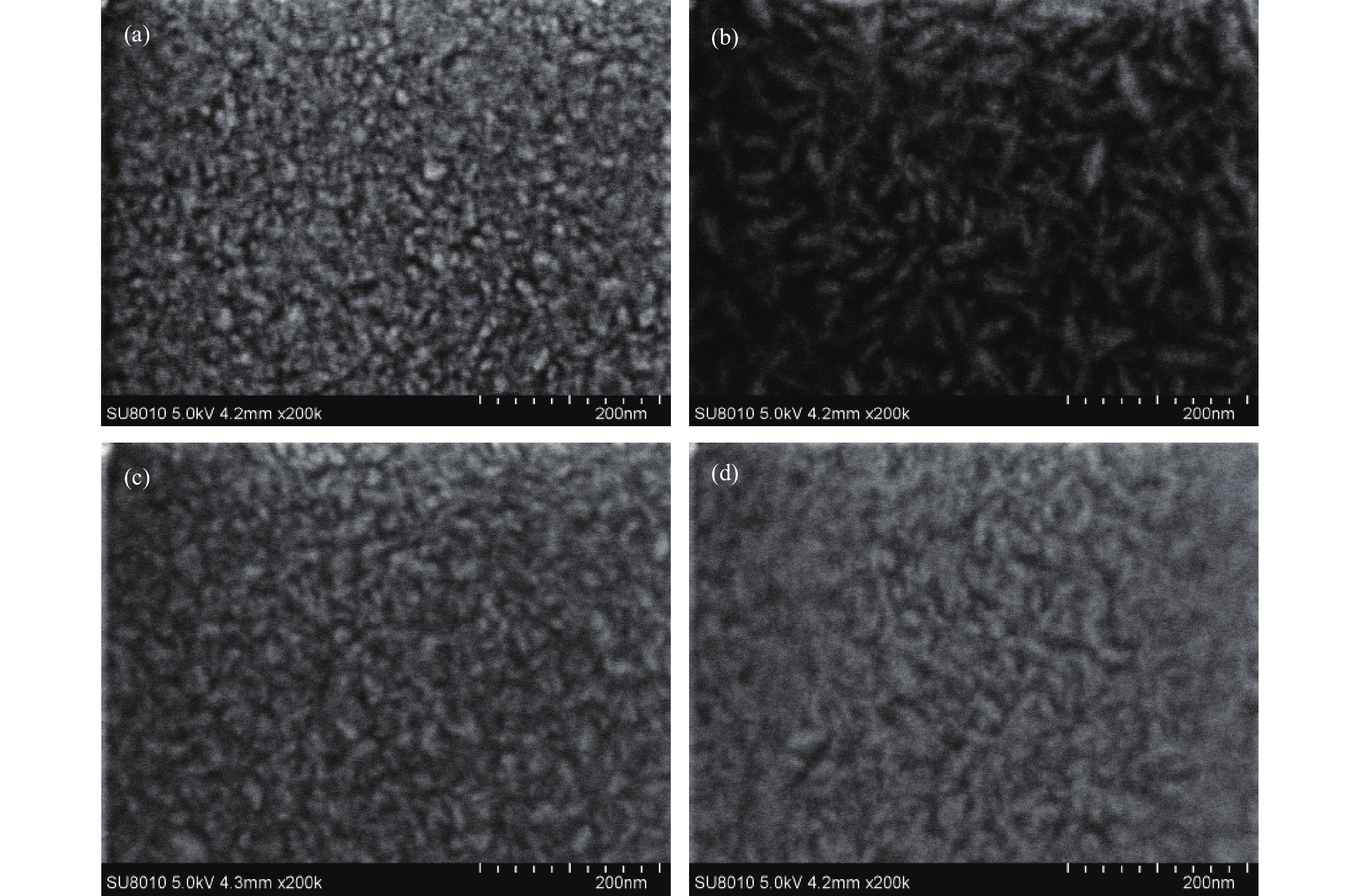
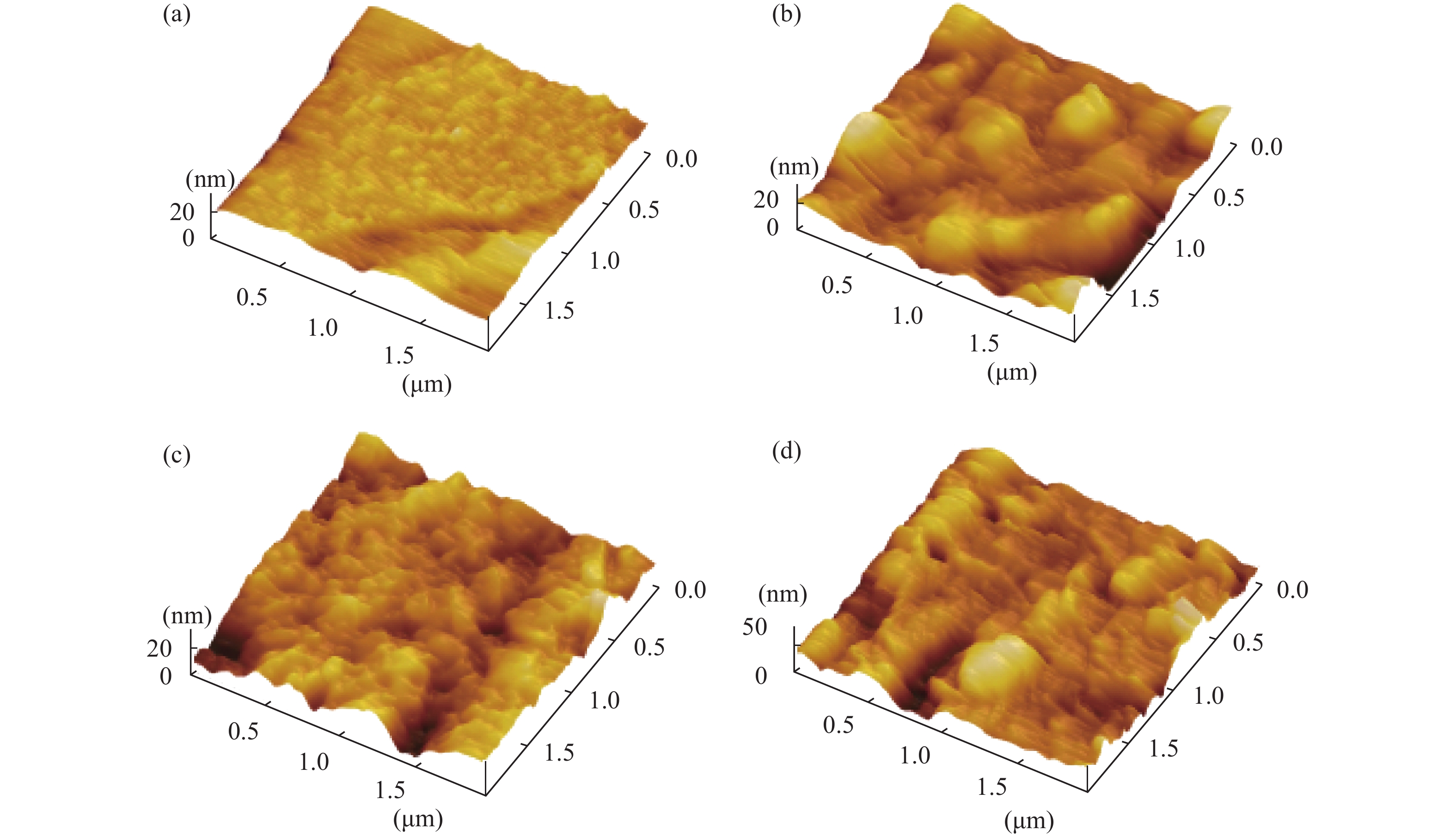
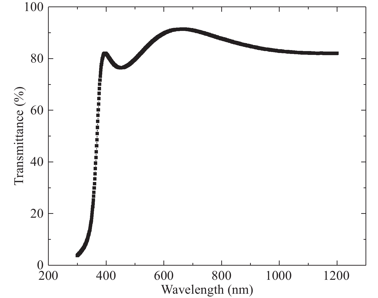
Table 1. Electrical properties of AZO thin films deposited at different temperatures.
| Temperature (°C) | Resistivity (Ω·cm) | Mobility (cm2/(V·s)) | Concentration (cm?3) | ||
| 100 | 8 × 101 | 0.26 | 1.67 × 10¹⁷ | ||
| 150 | 2.14 × 10?3 | 8.54 | 3.4 × 10²⁰ | ||
| 200 | 3.86 × 10?3 | 15.5 | 8.2 × 10¹⁹ | ||
| 250 | 4.23 × 10?3 | 9.48 | 1.84 × 10²⁰ |
 DownLoad: CSV
Table 2. Electrical properties of AZO thin films deposited at different Zn:Al cycle ratios.
| Zn : Al ratio | Resistivity (Ω·cm) | Mobility (cm2/(V·s)) | Concentration (cm?3) | ||
| 20 : 0 | 7.07 × 101 | 13 | 6.8 × 10¹⁵ | ||
| 20 : 1 | 7.09 × 10?2 | 2.13 | 4.1 × 10¹⁹ | ||
| 20 : 2 | 2.14 × 10?3 | 8.54 | 3.4 × 10²⁰ | ||
| 20 : 3 | 2.54 | 0.623 | 3.9 × 10¹⁹ |
DownLoad: CSV
| [1] |
Kim H, Gilmore C M, Gilmore J S, et al. Transparent conducting aluminum-doped zinc oxide thin films for organic light-emitting devices. Appl Phys Lett, 2000, 76: 259 doi: 10.1063/1.125740
|
| [2] |
Nomura K, Ohta H, Takagi A, et al. Room-temperature fabrication of transparent flexible thin-film transistors using amorphous oxide semiconductors. Nature, 2004, 432: 488 doi: 10.1038/nature03090
|
| [3] |
Minami T. Transparent conducting oxide semiconductors for transparent electrodes. Semicond Sci Technol, 2005, 20: 35 doi: 10.1088/0268-1242/20/4/004
|
| [4] |
Du X, George S M. Thickness dependence of sensor response for CO gas sensing by tin oxide films grown using atomic layer deposition. Sens Actuator B, 2008, 135: 152 doi: 10.1016/j.snb.2008.08.015
|
| [5] |
Martinson A B F, Elam J W, Hupp J T, et al. ZnO nanotube based dye-sensitized solar cells. Nano Lett, 2007, 7: 2183 doi: 10.1021/nl070160+
|
| [6] |
Meyer J, Gorrn P, Hamwi S, et al. Indium-free transparent organic light emitting diodes with Al doped ZnO electrodes grown by atomic layer and pulsed laser deposition. Appl Phys Lett, 2008, 93: 073308 doi: 10.1063/1.2975176
|
| [7] |
Lim J, Lee C. Effects of substrate temperature on the microstructure and photoluminescence properties of ZnO thin films prepared by atomic layer deposition. Thin Solid Films, 2007, 515: 3335 doi: 10.1016/j.tsf.2006.09.007
|
| [8] |
Ellmer K, Klein A, Rech B. Transparent conductive zinc oxide. Berlin: Springer, 2008
|
| [9] |
Granqvist C G. Transparent conductors as solar energy materials: a panoramic review. Sol Energy Mater Sol Cells, 2007, 91: 1529 doi: 10.1016/j.solmat.2007.04.031
|
| [10] |
Godlewski M, Guziewicz E, Luka G, et al. ZnO layers grown by atomic layer deposition: a new material for transparent conductive oxide. Thin Solid Films, 2009, 518: 1145 doi: 10.1016/j.tsf.2009.04.066
|
| [11] |
Duenow J N, Gessert T A, Wood D M, et al. Transparent conducting zinc oxide thin films doped with aluminum and molybdenum. J Vac Sci Technol A, 2007, 25: 955
|
| [12] |
Minami T, Nanto H, Takata S. Highly conductive and transparent Aluminum doped zinc oxide thin films prepared by RF magnetron sputtering. J Appl Phys, 1984, 23: 280 doi: 10.1143/JJAP.23.L280
|
| [13] |
Ohyama M, Ohyama H, Yoko T, et al. Sol-gel preparation of transparent and conductive aluminum-doped zinc oxide films with highly preferential crystal orientation. Ceram Soc, 1998, 81: 1622
|
| [14] |
Lau W S, Fonash S J. Highly transparent and conducting zinc oxide films deposited by activated reactive evaporation. J Electron Mater, 1987, 16: 141 doi: 10.1007/BF02655478
|
| [15] |
Shan F K, Liu G X, Lee W J, et al. The role of oxygen vacancies in epitaxial-deposited ZnO thin films. J Appl Phys, 2007, 10: 1053106
|
| [16] |
Steinhauser J, Fay S, Oliveira N, et al. Opto-electronic properties of rough LP-CVD ZnO:B for use as TCO in thin-film silicon solar cells. Appl Phys Lett, 2007, 90: 142107 doi: 10.1063/1.2719158
|
| [17] |
Cho D H, Yang S, Byun C, et al. Transparent Al–Zn–Sn–O thin film transistors prepared at low temperature. Appl Phys Lett, 2008, 93: 142111 doi: 10.1063/1.2998612
|
| [18] |
Jeong S H, Lee J W, Lee S B, et al. Deposition of aluminum-doped zinc oxide films by RF magnetron sputtering and study of their structural, electrical and optical properties. Thin Solid Films, 2003, 435: 78 doi: 10.1016/S0040-6090(03)00376-6
|
| [19] |
Kim D K, Kim H B. Room temperature deposition of Al-doped ZnO thin films on glass by RF magnetron sputtering under different Ar gas pressure. J Alloys Compd, 2011, 509: 421 doi: 10.1016/j.jallcom.2010.09.047
|
| [20] |
Maeng W J, Kim S J, Park J S, et al. Low temperature atomic layer deposited Al-doped ZnO thin films and associated semiconducting properties. J Vac Sci Technol A, 2012, 30: 1210
|
| [21] |
Luka G, Krajewski T A, Witkowski B S, et al. Aluminum-doped zinc oxide films grown by atomic layer deposition for transparent electrode applications. J Mater Sci: Mater Electron, 2011, 22: 1810 doi: 10.1007/s10854-011-0367-0
|
| [22] |
Dasgupta N P, Neubert S, Lee W, et al. Atomic layer deposition of Al-doped ZnO films: effect of grain orientation on conductivity. Chem Mater, 2010, 22: 4769 doi: 10.1021/cm101227h
|
| [23] |
Bosio A, Romeo N, Mazzamuto S, et al. Polycrystalline CdTe thin films for photovoltaic applications. Prog Cryst Growth Charact Mater, 2006, 52: 247 doi: 10.1016/j.pcrysgrow.2006.09.001
|
| [24] |
Huby N, Ferrari S, Guziewicz E, et al. Electrical behavior of zinc oxide layers grown by low temperature atomic layer deposition. Appl Phys Lett, 2007, 92: 023502
|
| [25] |
Guziewicz E, Kowalik I A, Godlewski M, et al. Extremely low temperature growth of ZnO by atomic layer deposition. J Appl Phys, 2008, 103: 033515 doi: 10.1063/1.2836819
|
| [26] |
Luka G, Krajewski T A, Witkowski B S, et al. Aluminum-doped zinc oxide films grown by atomic layer deposition for transparent electrode applications. J Mater Sci: Mater Electron, 2011, 22: 1810 doi: 10.1007/s10854-011-0367-0
|
| [27] |
Ahn C H, Lee S Y, Cho H K. Influence of growth temperature on the electrical and structural characteristics ofconductive Al-doped ZnO thin films grown by atomic layer deposition. Thin Solid Films, 2013, 545: 106 doi: 10.1016/j.tsf.2013.07.045
|
| [28] |
Geng Y, Guo L, Xu S S, et al. Influence of Al doping on the properties of ZnO fhin films grown by atomic layer deposition. J Phys Chem C, 2011, 115: 12317 doi: 10.1021/jp2023567
|
| [29] |
Maeng W J, Kimand S J, Park J S, et al. Low temperature atomic layer deposited Al-doped ZnO thin films and associated semiconducting properties. J Vac Sci Technol B, 2012, 30: 031210 doi: 10.1116/1.4710519
|
| [30] |
Elam J W, George S M. Growth of ZnO/Al2O3 alloy films using atomic layer deposition techniques. Chem Mater, 2003, 15: 1020 doi: 10.1021/cm020607+
|
| [31] |
Groner M D, Fabreguette F H, Elam J W, et al. Low-temperature Al2O3 atomic layer deposition. Chem Mater, 2004, 16: 639 doi: 10.1021/cm0304546
|
| [32] |
Guziewicz E, Kowalik I A, Godlewski M, et al. Extremely low temperature growth of ZnO by atomic layer deposition. J Appl Phys, 2008, 103: 033515 doi: 10.1063/1.2836819
|
| [33] |
Kim S K, Hwang C S, Par S H K, et al. Comparison between ZnO films grown by atomic layer deposition using H2O or O3 as oxidant. Thin Solid Films, 2005, 478: 103 doi: 10.1016/j.tsf.2004.10.015
|
| [34] |
Banerjee P, Lee W J, Bae K R, et al. Structural, electrical, and optical properties of atomic layer deposition Al-doped ZnO films. J Appl Phys, 2010, 108: 043504 doi: 10.1063/1.3466987
|
| [35] |
Dhakal T, Vanhart D, Christian R, et al. Growth morphology and electrical/optical properties of Al-doped ZnO thin films grown by atomic layer deposition. J Vac Sci Technol A, 2012, 30: 021202
|
| [36] |
Luka G, Krajewski T A, Witkowski B S, et al. Aluminum-doped zinc oxide films grown by atomic layer deposition for transparent electrode applications. J Mater Sci: Mater Electron, 2011, 22: 1810 doi: 10.1007/s10854-011-0367-0
|
| [37] |
Lim J, Lee C. Effects of substrate temperature on the microstructure and photoluminescence properties of ZnO thin films prepared by atomic layer deposition. Thin Solid Films, 2007, 515: 3335 doi: 10.1016/j.tsf.2006.09.007
|
| [38] |
Hultqvist A, Aitola K, Sveinbjornsson K, et al. Atomic layer deposition of electron selective SnOx and ZnO films on mixed halide perovskite: compatibility and performance. ACS Appl Mater Interfaces, 2017, 9(35): 29707 doi: 10.1021/acsami.7b07627
|
| [39] |
Liu H, Liu Y, Xiong P, et al. Aluminum-doped zinc oxide transparent electrode prepared by atomic layer deposition for organic light emitting devices. IEEE Trans Nanotechnol, 2017, 16: 634 doi: 10.1109/TNANO.2017.2700408
|


Article views: 4051 Times PDF downloads: 55 Times Cited by: 0 Times
Received: 05 June 2017 Revised: 18 September 2017 Online: Accepted Manuscript: 15 November 2017Uncorrected proof: 24 January 2018Published: 01 March 2018
| Citation: |
Li Chen, Xinliang Chen, Zhongxin Zhou, Sheng Guo, Ying Zhao, Xiaodan Zhang. Studies on morphology, electrical and optical characteristics of Al-doped ZnO thin films grown by atomic layer deposition[J]. Journal of Semiconductors, 2018, 39(3): 033004. doi: 10.1088/1674-4926/39/3/033004
****
L Chen, X L Chen, Z X Zhou, S Guo, Y Zhao, X D Zhang. Studies on morphology, electrical and optical characteristics of Al-doped ZnO thin films grown by atomic layer deposition[J]. J. Semicond., 2018, 39(3): 033004. doi: 10.1088/1674-4926/39/3/033004.

|
Project supported by the State Key Development Program for Basic Research of China (Nos. 2011CBA00706, 2011CBA00707) and the Tianjin Applied Basic Research Project and Cutting-Edge Technology Research Plan (No. 13JCZDJC26900).
| [1] |
Kim H, Gilmore C M, Gilmore J S, et al. Transparent conducting aluminum-doped zinc oxide thin films for organic light-emitting devices. Appl Phys Lett, 2000, 76: 259 doi: 10.1063/1.125740
|
| [2] |
Nomura K, Ohta H, Takagi A, et al. Room-temperature fabrication of transparent flexible thin-film transistors using amorphous oxide semiconductors. Nature, 2004, 432: 488 doi: 10.1038/nature03090
|
| [3] |
Minami T. Transparent conducting oxide semiconductors for transparent electrodes. Semicond Sci Technol, 2005, 20: 35 doi: 10.1088/0268-1242/20/4/004
|
| [4] |
Du X, George S M. Thickness dependence of sensor response for CO gas sensing by tin oxide films grown using atomic layer deposition. Sens Actuator B, 2008, 135: 152 doi: 10.1016/j.snb.2008.08.015
|
| [5] |
Martinson A B F, Elam J W, Hupp J T, et al. ZnO nanotube based dye-sensitized solar cells. Nano Lett, 2007, 7: 2183 doi: 10.1021/nl070160+
|
| [6] |
Meyer J, Gorrn P, Hamwi S, et al. Indium-free transparent organic light emitting diodes with Al doped ZnO electrodes grown by atomic layer and pulsed laser deposition. Appl Phys Lett, 2008, 93: 073308 doi: 10.1063/1.2975176
|
| [7] |
Lim J, Lee C. Effects of substrate temperature on the microstructure and photoluminescence properties of ZnO thin films prepared by atomic layer deposition. Thin Solid Films, 2007, 515: 3335 doi: 10.1016/j.tsf.2006.09.007
|
| [8] |
Ellmer K, Klein A, Rech B. Transparent conductive zinc oxide. Berlin: Springer, 2008
|
| [9] |
Granqvist C G. Transparent conductors as solar energy materials: a panoramic review. Sol Energy Mater Sol Cells, 2007, 91: 1529 doi: 10.1016/j.solmat.2007.04.031
|
| [10] |
Godlewski M, Guziewicz E, Luka G, et al. ZnO layers grown by atomic layer deposition: a new material for transparent conductive oxide. Thin Solid Films, 2009, 518: 1145 doi: 10.1016/j.tsf.2009.04.066
|
| [11] |
Duenow J N, Gessert T A, Wood D M, et al. Transparent conducting zinc oxide thin films doped with aluminum and molybdenum. J Vac Sci Technol A, 2007, 25: 955
|
| [12] |
Minami T, Nanto H, Takata S. Highly conductive and transparent Aluminum doped zinc oxide thin films prepared by RF magnetron sputtering. J Appl Phys, 1984, 23: 280 doi: 10.1143/JJAP.23.L280
|
| [13] |
Ohyama M, Ohyama H, Yoko T, et al. Sol-gel preparation of transparent and conductive aluminum-doped zinc oxide films with highly preferential crystal orientation. Ceram Soc, 1998, 81: 1622
|
| [14] |
Lau W S, Fonash S J. Highly transparent and conducting zinc oxide films deposited by activated reactive evaporation. J Electron Mater, 1987, 16: 141 doi: 10.1007/BF02655478
|
| [15] |
Shan F K, Liu G X, Lee W J, et al. The role of oxygen vacancies in epitaxial-deposited ZnO thin films. J Appl Phys, 2007, 10: 1053106
|
| [16] |
Steinhauser J, Fay S, Oliveira N, et al. Opto-electronic properties of rough LP-CVD ZnO:B for use as TCO in thin-film silicon solar cells. Appl Phys Lett, 2007, 90: 142107 doi: 10.1063/1.2719158
|
| [17] |
Cho D H, Yang S, Byun C, et al. Transparent Al–Zn–Sn–O thin film transistors prepared at low temperature. Appl Phys Lett, 2008, 93: 142111 doi: 10.1063/1.2998612
|
| [18] |
Jeong S H, Lee J W, Lee S B, et al. Deposition of aluminum-doped zinc oxide films by RF magnetron sputtering and study of their structural, electrical and optical properties. Thin Solid Films, 2003, 435: 78 doi: 10.1016/S0040-6090(03)00376-6
|
| [19] |
Kim D K, Kim H B. Room temperature deposition of Al-doped ZnO thin films on glass by RF magnetron sputtering under different Ar gas pressure. J Alloys Compd, 2011, 509: 421 doi: 10.1016/j.jallcom.2010.09.047
|
| [20] |
Maeng W J, Kim S J, Park J S, et al. Low temperature atomic layer deposited Al-doped ZnO thin films and associated semiconducting properties. J Vac Sci Technol A, 2012, 30: 1210
|
| [21] |
Luka G, Krajewski T A, Witkowski B S, et al. Aluminum-doped zinc oxide films grown by atomic layer deposition for transparent electrode applications. J Mater Sci: Mater Electron, 2011, 22: 1810 doi: 10.1007/s10854-011-0367-0
|
| [22] |
Dasgupta N P, Neubert S, Lee W, et al. Atomic layer deposition of Al-doped ZnO films: effect of grain orientation on conductivity. Chem Mater, 2010, 22: 4769 doi: 10.1021/cm101227h
|
| [23] |
Bosio A, Romeo N, Mazzamuto S, et al. Polycrystalline CdTe thin films for photovoltaic applications. Prog Cryst Growth Charact Mater, 2006, 52: 247 doi: 10.1016/j.pcrysgrow.2006.09.001
|
| [24] |
Huby N, Ferrari S, Guziewicz E, et al. Electrical behavior of zinc oxide layers grown by low temperature atomic layer deposition. Appl Phys Lett, 2007, 92: 023502
|
| [25] |
Guziewicz E, Kowalik I A, Godlewski M, et al. Extremely low temperature growth of ZnO by atomic layer deposition. J Appl Phys, 2008, 103: 033515 doi: 10.1063/1.2836819
|
| [26] |
Luka G, Krajewski T A, Witkowski B S, et al. Aluminum-doped zinc oxide films grown by atomic layer deposition for transparent electrode applications. J Mater Sci: Mater Electron, 2011, 22: 1810 doi: 10.1007/s10854-011-0367-0
|
| [27] |
Ahn C H, Lee S Y, Cho H K. Influence of growth temperature on the electrical and structural characteristics ofconductive Al-doped ZnO thin films grown by atomic layer deposition. Thin Solid Films, 2013, 545: 106 doi: 10.1016/j.tsf.2013.07.045
|
| [28] |
Geng Y, Guo L, Xu S S, et al. Influence of Al doping on the properties of ZnO fhin films grown by atomic layer deposition. J Phys Chem C, 2011, 115: 12317 doi: 10.1021/jp2023567
|
| [29] |
Maeng W J, Kimand S J, Park J S, et al. Low temperature atomic layer deposited Al-doped ZnO thin films and associated semiconducting properties. J Vac Sci Technol B, 2012, 30: 031210 doi: 10.1116/1.4710519
|
| [30] |
Elam J W, George S M. Growth of ZnO/Al2O3 alloy films using atomic layer deposition techniques. Chem Mater, 2003, 15: 1020 doi: 10.1021/cm020607+
|
| [31] |
Groner M D, Fabreguette F H, Elam J W, et al. Low-temperature Al2O3 atomic layer deposition. Chem Mater, 2004, 16: 639 doi: 10.1021/cm0304546
|
| [32] |
Guziewicz E, Kowalik I A, Godlewski M, et al. Extremely low temperature growth of ZnO by atomic layer deposition. J Appl Phys, 2008, 103: 033515 doi: 10.1063/1.2836819
|
| [33] |
Kim S K, Hwang C S, Par S H K, et al. Comparison between ZnO films grown by atomic layer deposition using H2O or O3 as oxidant. Thin Solid Films, 2005, 478: 103 doi: 10.1016/j.tsf.2004.10.015
|
| [34] |
Banerjee P, Lee W J, Bae K R, et al. Structural, electrical, and optical properties of atomic layer deposition Al-doped ZnO films. J Appl Phys, 2010, 108: 043504 doi: 10.1063/1.3466987
|
| [35] |
Dhakal T, Vanhart D, Christian R, et al. Growth morphology and electrical/optical properties of Al-doped ZnO thin films grown by atomic layer deposition. J Vac Sci Technol A, 2012, 30: 021202
|
| [36] |
Luka G, Krajewski T A, Witkowski B S, et al. Aluminum-doped zinc oxide films grown by atomic layer deposition for transparent electrode applications. J Mater Sci: Mater Electron, 2011, 22: 1810 doi: 10.1007/s10854-011-0367-0
|
| [37] |
Lim J, Lee C. Effects of substrate temperature on the microstructure and photoluminescence properties of ZnO thin films prepared by atomic layer deposition. Thin Solid Films, 2007, 515: 3335 doi: 10.1016/j.tsf.2006.09.007
|
| [38] |
Hultqvist A, Aitola K, Sveinbjornsson K, et al. Atomic layer deposition of electron selective SnOx and ZnO films on mixed halide perovskite: compatibility and performance. ACS Appl Mater Interfaces, 2017, 9(35): 29707 doi: 10.1021/acsami.7b07627
|
| [39] |
Liu H, Liu Y, Xiong P, et al. Aluminum-doped zinc oxide transparent electrode prepared by atomic layer deposition for organic light emitting devices. IEEE Trans Nanotechnol, 2017, 16: 634 doi: 10.1109/TNANO.2017.2700408
|

 WeChat ID
Journal of Semiconductors © 2017 All Rights Reserved 京ICP備05085259號(hào)-2