


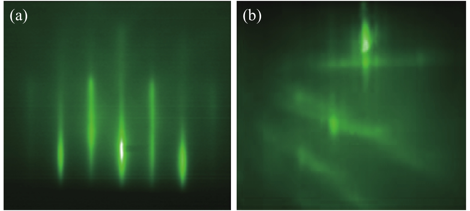
Fig. 1.
(Color online) InAs1–xSbx layer RHEED pattern (a) (× 1) pattern and (b) (× 3) pattern.
SEMICONDUCTOR MATERIALS
D. Benyahia1, , ?. Kubiszyn2, K. Michalczewski1, A. K?b?owski2, P. Martyniuk1, J. Piotrowski2 and A. Rogalski1
Corresponding author: D. Benyahia, Email: djalelbeny@gmail.com
Abstract: Undoped and Be-doped InAs1–xSbx (0 ≤ x ≤ 0.71) epitaxial layers were successfully grown on lattice mismatched semi-insulating GaAs (001) substrate with 2° offcut towards <110>. The effect of the InAs buffer layer on the quality of the grown layers was investigated. Moreover, the influence of Sb/In flux ratio on the Sb fraction was examined. Furthermore, we have studied the defects distribution along the depth of the InAsSb epilayers. In addition, the p-type doping of the grown layers was explored. The InAsSb layers were assessed by X-ray diffraction, Nomarski microscopy, high resolution optical microscopy and Hall effect measurement. The InAs buffer layer was found to be beneficial for the growth of high quality InAsSb layers. The X-ray analysis revealed a full width at half maximum (FWHM) of 571 arcsec for InAs 0.87Sb0.13. It is worth noting here that the Hall concentration (mobility) as low (high) as 5 × 1016 cm?3 (25000 cm2V?1s?1) at room temperature, has been acquired.
Key words: MBE, InAsSb, Hall effect, GaAs, X-ray diffraction
| [1] |
Wooley J C, Warner J. Optical energy-gap variation in InAs-InSb alloys. Can J Phys, 1964, 42: 1879 doi: 10.1139/p64-176
|
| [2] |
Bethea C G, Yen M Y, Levine B F, et al. Long wavelength InAs1–xSbx/GaAs detectors prepared by molecular beam epitaxy. Appl Phys Lett, 1987, 51: 1431 doi: 10.1063/1.98647
|
| [3] |
Dobbelaere W, De Boeck J, Borghs G. Growth and optical characterization of InAs1–xSbx (0 ≤ x ≤ 1) on GaAs and GaAs-coated Si by molecular beam epitaxy. Appl Phys Lett, 1989, 55: 1856 doi: 10.1063/1.102187
|
| [4] |
Dobbelaere W, De Boeck J, Bruynseraede C, et al. InAsSb light emitting diodes and their applications to infrared gas senors. Electron Let, 1993, 29: 890 doi: 10.1049/el:19930594
|
| [5] |
Biefeld R M. The metal–organic chemical vapor deposition and properties of III–V antimony-based semiconductor materials. Mater Sci Eng, 2002, R 36: 105
|
| [6] |
Yen M Y, People R, Wecht K W. Long wavelength (3–5 and 8–12 μm) photoluminescence of InAs1–xSbx grown on (100) GaAs by molecular beam epitaxy. J Appl Phys, 1988, 64: 952 doi: 10.1063/1.341904
|
| [7] |
Gao H, Wang W, Jiang Z, et al. The growth parameter influence on the crystal quality of InAsSb grown on GaAs by molecular beam epitaxy. J Cryst Growth, 2007, 308: 406 doi: 10.1016/j.jcrysgro.2007.08.018
|
| [8] |
Nakamura S, Jayavel P, Koyama T, et al. Investigations on the effect of InSb and InAsSb step-graded buffer layers in InAs0.5Sb0.5 epilayers grown on GaAs (001). J Cryst Growth, 2007, 300: 497 doi: 10.1016/j.jcrysgro.2006.11.298
|
| [9] |
Yen M Y, Levine B F, Bethea C G, et al. Molecular beam epitaxial growth and optical properties of InAs1–xSbx in 8–12 μm wavelength range. Appl Phys Lett, 1987, 50: 927 doi: 10.1063/1.97982
|
| [10] |
Chyi J I, Kalem S, Kumar N S, et al. Growth of InSb and InAs1–xSbx on GaAs by molecular beam epitaxy. Appl Phys Lett, 1988, 53: 1092 doi: 10.1063/1.100031
|
| [11] |
Tsukamoto S, Bhattacharya P, Chen Y C, et al. Transport properties of InAs1–xSbx (0 ≤ x ≤ 0.55) on InP grown by molecular beam epitaxy. J Appl Phys, 1990, 67: 6819 doi: 10.1063/1.345071
|
| [12] |
Chiang P K, Bedair S M. Growth of InSb and InAs1–xSbx by OM-CVD. J Electrochem Soc, 1984, 131: 2422 doi: 10.1149/1.2115308
|
| [13] |
Chiang P K, Bedair S M. p–n junction in InSb and InAs1–xSbx by metalorganic chemical vapor deposition. Appl Phys Lett, 1985, 46: 383 doi: 10.1063/1.95640
|
| [14] |
Biefeld R M, Hills C R, Lee S R. Strain relief in compositionally graded InAs1–xSbx buffer layers and InAxSb1–x/InSb strained-layer superlattices grown by MOCVD. J Cryst Growth, 1988, 91: 515 doi: 10.1016/0022-0248(88)90119-4
|
| [15] |
Kim J D, Wu D, Wojkowski J, et al. Long-wavelength InAsSb photoconductors operated at near room temperatures (200–300 K). Appl Phys Lett, 1996, 68: 99 doi: 10.1063/1.116784
|
| [16] |
Mao Y, Krier A. Liquid phase epitaxial growth and photoluminescence of InAsSb grown on GaSb substrates from antimony solution. J Cryst Growth, 1993, 133: 108 doi: 10.1016/0022-0248(93)90110-I
|
| [17] |
Gao F, Chen N, Liu L, et al. InAs0.3Sb0.7 films grown on (100) GaSb substrates with a buffer layer by liquid phase epitaxy. J Cryst Growth, 2007, 304: 472 doi: 10.1016/j.jcrysgro.2007.03.011
|
| [18] |
Shanabrook B V, Waterman J R, Davis J L, et al. Large temperature changes induced by molecular beam epitaxial growth on radiatively heated substrates. Appl Phys Lett, 1992, 61: 2338 doi: 10.1063/1.108236
|
| [19] |
Benyahia D, Kubiszyn L, Michalczewski K, et al. Molecular beam epitaxial growth and characterization of InAs layers on GaAs (001) substrate. Opt Quant Elect, 2016, 48: 428 doi: 10.1007/s11082-016-0698-4
|
| [20] |
Marcadet X, Rakovska A, Prevot I, et al. MBE growth of room-temperature InAsSb mid-infrared detectors. J Cryst Growth, 2001, 227: 609
|
| [21] |
Sun Q L, Wang L, Wang W Q, et al. Growth and characterization of InAs1–xsbx with different sb compositions on GaAs substrates. Chin Phys Lett, 2015, 32: 106801 doi: 10.1088/0256-307X/32/10/106801
|
| [22] |
Egan R J, Chin V W L, Tansley T L. Dislocation scattering effects on electron mobility of InAsSb. J Appl Phys, 1994, 75: 2473 doi: 10.1063/1.356244
|
| [23] |
Petriz R L. Theory of an experiment for measuring the mobility and density of carriers in the space-charge region of a semiconductor surface. Phys Rev, 1958, 110: 1254 doi: 10.1103/PhysRev.110.1254
|
| [24] |
Shinde U P. Hall coefficient, mobility and carrier concentration as a function of composition and thickness of Zn–Te thin films. Adv Appl Sci Res, 2015, 6: 215
|
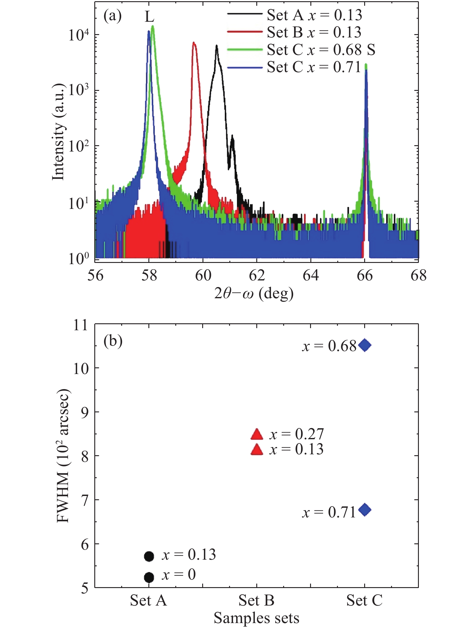
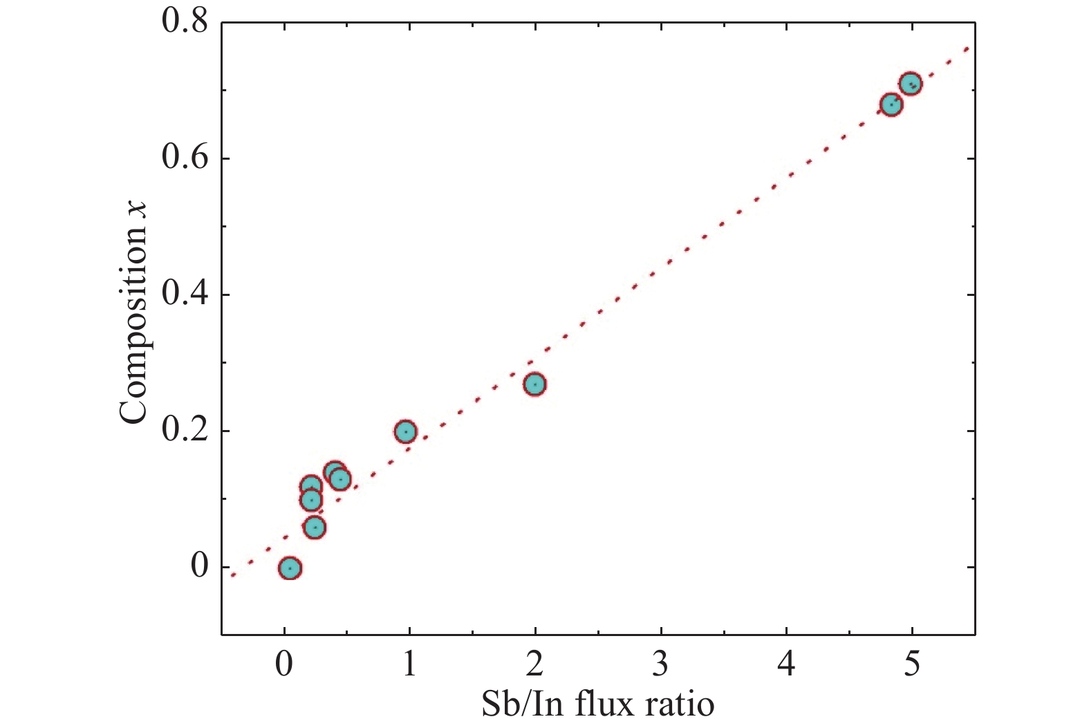
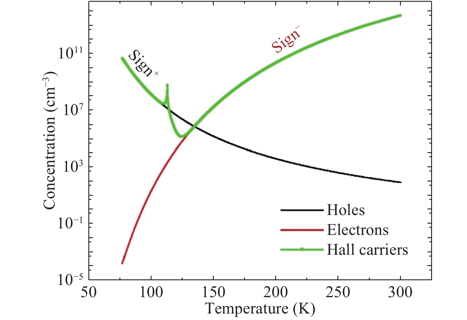
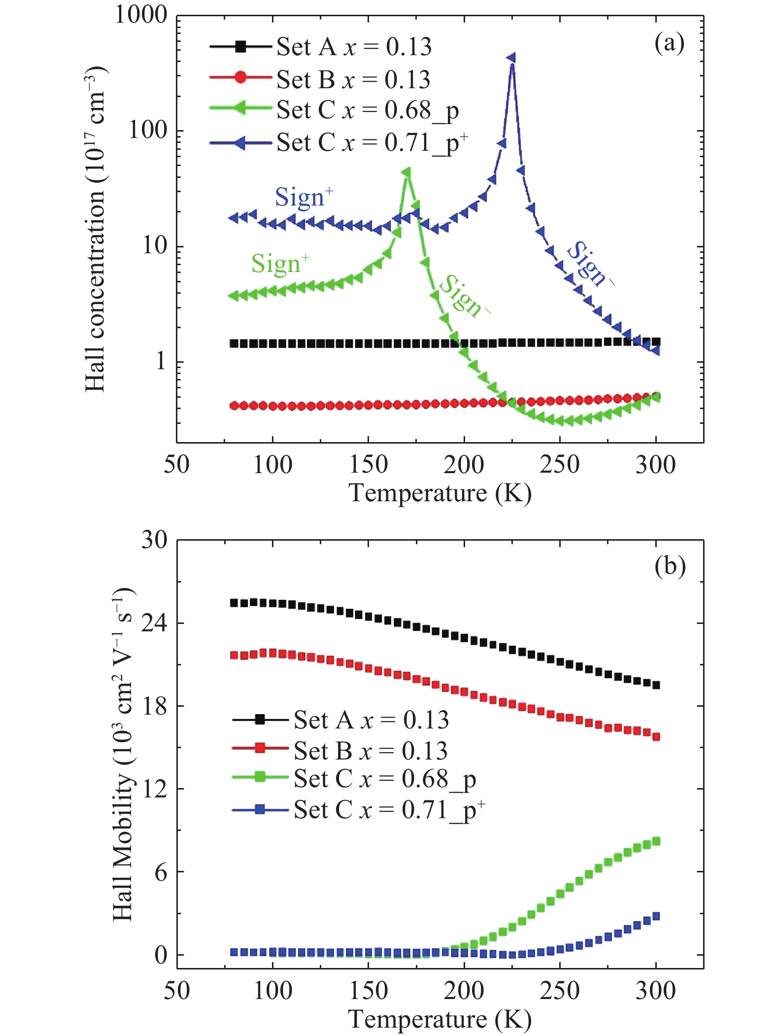
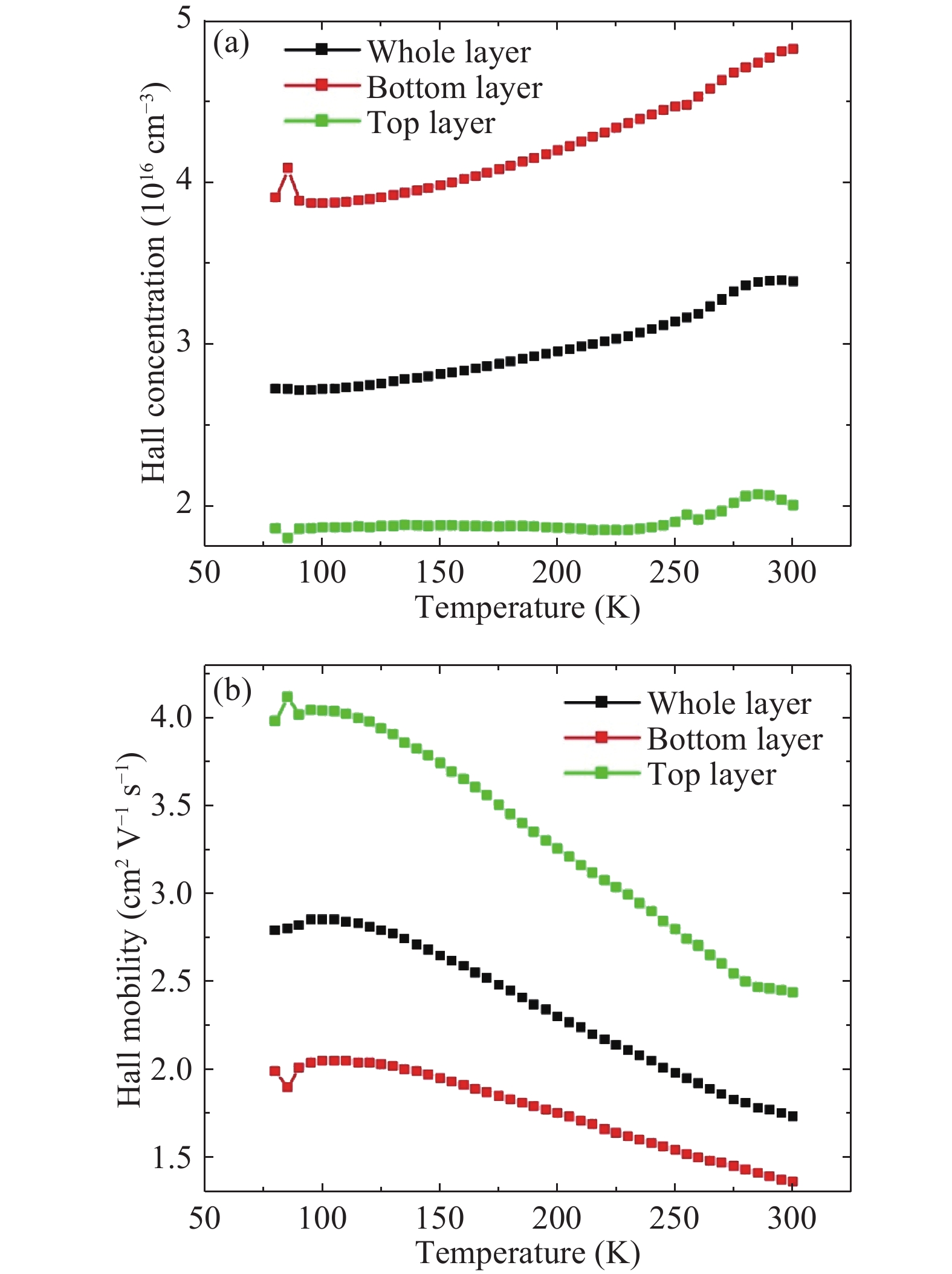
Table 1. InAs1–xSbx samples grown on GaAs (001) substrate.
| Sets | Buffer layer | Doping | Composition x |
| A | InAs | – | 0.13; 0.06; 0 |
| B | – | – | 0.13; 0.27 |
| C | – | Be | 0.68; 0.71 |
 DownLoad: CSV
| [1] |
Wooley J C, Warner J. Optical energy-gap variation in InAs-InSb alloys. Can J Phys, 1964, 42: 1879 doi: 10.1139/p64-176
|
| [2] |
Bethea C G, Yen M Y, Levine B F, et al. Long wavelength InAs1–xSbx/GaAs detectors prepared by molecular beam epitaxy. Appl Phys Lett, 1987, 51: 1431 doi: 10.1063/1.98647
|
| [3] |
Dobbelaere W, De Boeck J, Borghs G. Growth and optical characterization of InAs1–xSbx (0 ≤ x ≤ 1) on GaAs and GaAs-coated Si by molecular beam epitaxy. Appl Phys Lett, 1989, 55: 1856 doi: 10.1063/1.102187
|
| [4] |
Dobbelaere W, De Boeck J, Bruynseraede C, et al. InAsSb light emitting diodes and their applications to infrared gas senors. Electron Let, 1993, 29: 890 doi: 10.1049/el:19930594
|
| [5] |
Biefeld R M. The metal–organic chemical vapor deposition and properties of III–V antimony-based semiconductor materials. Mater Sci Eng, 2002, R 36: 105
|
| [6] |
Yen M Y, People R, Wecht K W. Long wavelength (3–5 and 8–12 μm) photoluminescence of InAs1–xSbx grown on (100) GaAs by molecular beam epitaxy. J Appl Phys, 1988, 64: 952 doi: 10.1063/1.341904
|
| [7] |
Gao H, Wang W, Jiang Z, et al. The growth parameter influence on the crystal quality of InAsSb grown on GaAs by molecular beam epitaxy. J Cryst Growth, 2007, 308: 406 doi: 10.1016/j.jcrysgro.2007.08.018
|
| [8] |
Nakamura S, Jayavel P, Koyama T, et al. Investigations on the effect of InSb and InAsSb step-graded buffer layers in InAs0.5Sb0.5 epilayers grown on GaAs (001). J Cryst Growth, 2007, 300: 497 doi: 10.1016/j.jcrysgro.2006.11.298
|
| [9] |
Yen M Y, Levine B F, Bethea C G, et al. Molecular beam epitaxial growth and optical properties of InAs1–xSbx in 8–12 μm wavelength range. Appl Phys Lett, 1987, 50: 927 doi: 10.1063/1.97982
|
| [10] |
Chyi J I, Kalem S, Kumar N S, et al. Growth of InSb and InAs1–xSbx on GaAs by molecular beam epitaxy. Appl Phys Lett, 1988, 53: 1092 doi: 10.1063/1.100031
|
| [11] |
Tsukamoto S, Bhattacharya P, Chen Y C, et al. Transport properties of InAs1–xSbx (0 ≤ x ≤ 0.55) on InP grown by molecular beam epitaxy. J Appl Phys, 1990, 67: 6819 doi: 10.1063/1.345071
|
| [12] |
Chiang P K, Bedair S M. Growth of InSb and InAs1–xSbx by OM-CVD. J Electrochem Soc, 1984, 131: 2422 doi: 10.1149/1.2115308
|
| [13] |
Chiang P K, Bedair S M. p–n junction in InSb and InAs1–xSbx by metalorganic chemical vapor deposition. Appl Phys Lett, 1985, 46: 383 doi: 10.1063/1.95640
|
| [14] |
Biefeld R M, Hills C R, Lee S R. Strain relief in compositionally graded InAs1–xSbx buffer layers and InAxSb1–x/InSb strained-layer superlattices grown by MOCVD. J Cryst Growth, 1988, 91: 515 doi: 10.1016/0022-0248(88)90119-4
|
| [15] |
Kim J D, Wu D, Wojkowski J, et al. Long-wavelength InAsSb photoconductors operated at near room temperatures (200–300 K). Appl Phys Lett, 1996, 68: 99 doi: 10.1063/1.116784
|
| [16] |
Mao Y, Krier A. Liquid phase epitaxial growth and photoluminescence of InAsSb grown on GaSb substrates from antimony solution. J Cryst Growth, 1993, 133: 108 doi: 10.1016/0022-0248(93)90110-I
|
| [17] |
Gao F, Chen N, Liu L, et al. InAs0.3Sb0.7 films grown on (100) GaSb substrates with a buffer layer by liquid phase epitaxy. J Cryst Growth, 2007, 304: 472 doi: 10.1016/j.jcrysgro.2007.03.011
|
| [18] |
Shanabrook B V, Waterman J R, Davis J L, et al. Large temperature changes induced by molecular beam epitaxial growth on radiatively heated substrates. Appl Phys Lett, 1992, 61: 2338 doi: 10.1063/1.108236
|
| [19] |
Benyahia D, Kubiszyn L, Michalczewski K, et al. Molecular beam epitaxial growth and characterization of InAs layers on GaAs (001) substrate. Opt Quant Elect, 2016, 48: 428 doi: 10.1007/s11082-016-0698-4
|
| [20] |
Marcadet X, Rakovska A, Prevot I, et al. MBE growth of room-temperature InAsSb mid-infrared detectors. J Cryst Growth, 2001, 227: 609
|
| [21] |
Sun Q L, Wang L, Wang W Q, et al. Growth and characterization of InAs1–xsbx with different sb compositions on GaAs substrates. Chin Phys Lett, 2015, 32: 106801 doi: 10.1088/0256-307X/32/10/106801
|
| [22] |
Egan R J, Chin V W L, Tansley T L. Dislocation scattering effects on electron mobility of InAsSb. J Appl Phys, 1994, 75: 2473 doi: 10.1063/1.356244
|
| [23] |
Petriz R L. Theory of an experiment for measuring the mobility and density of carriers in the space-charge region of a semiconductor surface. Phys Rev, 1958, 110: 1254 doi: 10.1103/PhysRev.110.1254
|
| [24] |
Shinde U P. Hall coefficient, mobility and carrier concentration as a function of composition and thickness of Zn–Te thin films. Adv Appl Sci Res, 2015, 6: 215
|


Article views: 4183 Times PDF downloads: 88 Times Cited by: 0 Times
Received: 02 June 2017 Revised: 02 October 2017 Online: Accepted Manuscript: 11 November 2017Uncorrected proof: 24 January 2018Published: 01 March 2018
| Citation: |
D. Benyahia, ?. Kubiszyn, K. Michalczewski, A. K?b?owski, P. Martyniuk, J. Piotrowski, A. Rogalski. Investigation on the InAs1–xSbx epilayers growth on GaAs (001) substrate by molecular beam epitaxy[J]. Journal of Semiconductors, 2018, 39(3): 033003. doi: 10.1088/1674-4926/39/3/033003
****
D. Benyahia, ?. Kubiszyn, K. Michalczewski, A. K?b?owski, P. Martyniuk, J. Piotrowski, A. Rogalski. Investigation on the InAs1–xSbx epilayers growth on GaAs (001) substrate by molecular beam epitaxy[J]. J. Semicond., 2018, 39(3): 033003. doi: 10.1088/1674-4926/39/3/033003.

|
Project supported by the Polish National Science Centre (No. UMO-2015/17/B/ST5/01753).
| [1] |
Wooley J C, Warner J. Optical energy-gap variation in InAs-InSb alloys. Can J Phys, 1964, 42: 1879 doi: 10.1139/p64-176
|
| [2] |
Bethea C G, Yen M Y, Levine B F, et al. Long wavelength InAs1–xSbx/GaAs detectors prepared by molecular beam epitaxy. Appl Phys Lett, 1987, 51: 1431 doi: 10.1063/1.98647
|
| [3] |
Dobbelaere W, De Boeck J, Borghs G. Growth and optical characterization of InAs1–xSbx (0 ≤ x ≤ 1) on GaAs and GaAs-coated Si by molecular beam epitaxy. Appl Phys Lett, 1989, 55: 1856 doi: 10.1063/1.102187
|
| [4] |
Dobbelaere W, De Boeck J, Bruynseraede C, et al. InAsSb light emitting diodes and their applications to infrared gas senors. Electron Let, 1993, 29: 890 doi: 10.1049/el:19930594
|
| [5] |
Biefeld R M. The metal–organic chemical vapor deposition and properties of III–V antimony-based semiconductor materials. Mater Sci Eng, 2002, R 36: 105
|
| [6] |
Yen M Y, People R, Wecht K W. Long wavelength (3–5 and 8–12 μm) photoluminescence of InAs1–xSbx grown on (100) GaAs by molecular beam epitaxy. J Appl Phys, 1988, 64: 952 doi: 10.1063/1.341904
|
| [7] |
Gao H, Wang W, Jiang Z, et al. The growth parameter influence on the crystal quality of InAsSb grown on GaAs by molecular beam epitaxy. J Cryst Growth, 2007, 308: 406 doi: 10.1016/j.jcrysgro.2007.08.018
|
| [8] |
Nakamura S, Jayavel P, Koyama T, et al. Investigations on the effect of InSb and InAsSb step-graded buffer layers in InAs0.5Sb0.5 epilayers grown on GaAs (001). J Cryst Growth, 2007, 300: 497 doi: 10.1016/j.jcrysgro.2006.11.298
|
| [9] |
Yen M Y, Levine B F, Bethea C G, et al. Molecular beam epitaxial growth and optical properties of InAs1–xSbx in 8–12 μm wavelength range. Appl Phys Lett, 1987, 50: 927 doi: 10.1063/1.97982
|
| [10] |
Chyi J I, Kalem S, Kumar N S, et al. Growth of InSb and InAs1–xSbx on GaAs by molecular beam epitaxy. Appl Phys Lett, 1988, 53: 1092 doi: 10.1063/1.100031
|
| [11] |
Tsukamoto S, Bhattacharya P, Chen Y C, et al. Transport properties of InAs1–xSbx (0 ≤ x ≤ 0.55) on InP grown by molecular beam epitaxy. J Appl Phys, 1990, 67: 6819 doi: 10.1063/1.345071
|
| [12] |
Chiang P K, Bedair S M. Growth of InSb and InAs1–xSbx by OM-CVD. J Electrochem Soc, 1984, 131: 2422 doi: 10.1149/1.2115308
|
| [13] |
Chiang P K, Bedair S M. p–n junction in InSb and InAs1–xSbx by metalorganic chemical vapor deposition. Appl Phys Lett, 1985, 46: 383 doi: 10.1063/1.95640
|
| [14] |
Biefeld R M, Hills C R, Lee S R. Strain relief in compositionally graded InAs1–xSbx buffer layers and InAxSb1–x/InSb strained-layer superlattices grown by MOCVD. J Cryst Growth, 1988, 91: 515 doi: 10.1016/0022-0248(88)90119-4
|
| [15] |
Kim J D, Wu D, Wojkowski J, et al. Long-wavelength InAsSb photoconductors operated at near room temperatures (200–300 K). Appl Phys Lett, 1996, 68: 99 doi: 10.1063/1.116784
|
| [16] |
Mao Y, Krier A. Liquid phase epitaxial growth and photoluminescence of InAsSb grown on GaSb substrates from antimony solution. J Cryst Growth, 1993, 133: 108 doi: 10.1016/0022-0248(93)90110-I
|
| [17] |
Gao F, Chen N, Liu L, et al. InAs0.3Sb0.7 films grown on (100) GaSb substrates with a buffer layer by liquid phase epitaxy. J Cryst Growth, 2007, 304: 472 doi: 10.1016/j.jcrysgro.2007.03.011
|
| [18] |
Shanabrook B V, Waterman J R, Davis J L, et al. Large temperature changes induced by molecular beam epitaxial growth on radiatively heated substrates. Appl Phys Lett, 1992, 61: 2338 doi: 10.1063/1.108236
|
| [19] |
Benyahia D, Kubiszyn L, Michalczewski K, et al. Molecular beam epitaxial growth and characterization of InAs layers on GaAs (001) substrate. Opt Quant Elect, 2016, 48: 428 doi: 10.1007/s11082-016-0698-4
|
| [20] |
Marcadet X, Rakovska A, Prevot I, et al. MBE growth of room-temperature InAsSb mid-infrared detectors. J Cryst Growth, 2001, 227: 609
|
| [21] |
Sun Q L, Wang L, Wang W Q, et al. Growth and characterization of InAs1–xsbx with different sb compositions on GaAs substrates. Chin Phys Lett, 2015, 32: 106801 doi: 10.1088/0256-307X/32/10/106801
|
| [22] |
Egan R J, Chin V W L, Tansley T L. Dislocation scattering effects on electron mobility of InAsSb. J Appl Phys, 1994, 75: 2473 doi: 10.1063/1.356244
|
| [23] |
Petriz R L. Theory of an experiment for measuring the mobility and density of carriers in the space-charge region of a semiconductor surface. Phys Rev, 1958, 110: 1254 doi: 10.1103/PhysRev.110.1254
|
| [24] |
Shinde U P. Hall coefficient, mobility and carrier concentration as a function of composition and thickness of Zn–Te thin films. Adv Appl Sci Res, 2015, 6: 215
|

 WeChat ID
Journal of Semiconductors © 2017 All Rights Reserved 京ICP備05085259號-2

