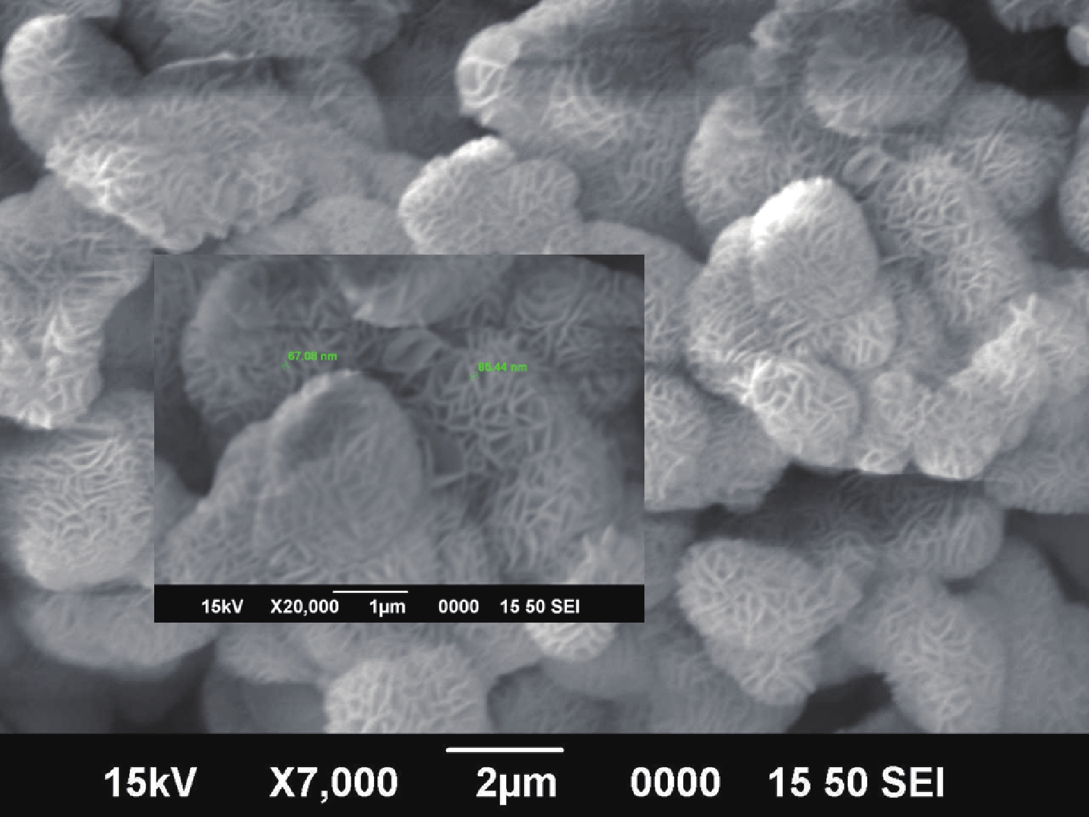
Fig. 1.
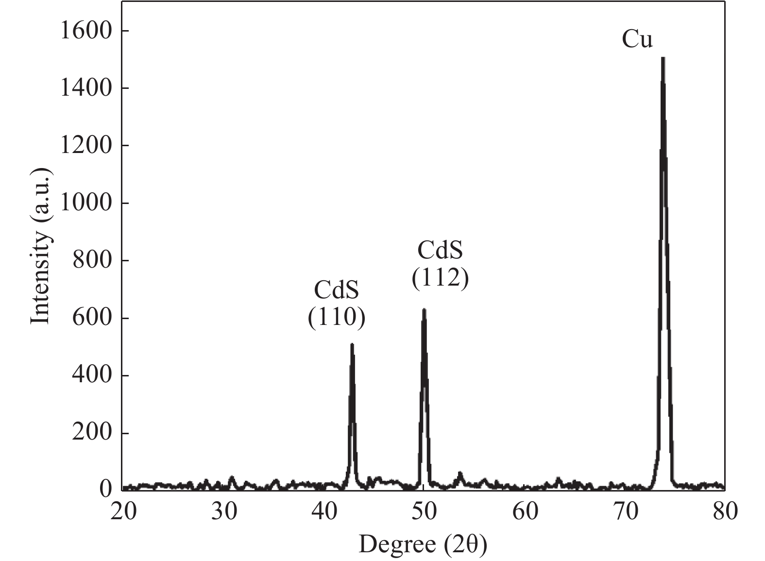
X-ray diffraction spectrum of the Cu/CdS structure.
SEMICONDUCTOR MATERIALS
R. Jayakrishnan, Varun G Nair, Akhil M Anand and Meera Venugopal
Corresponding author: R. Jayakrishnan, Email: rjayakrishnan2002@yahoo.co.in
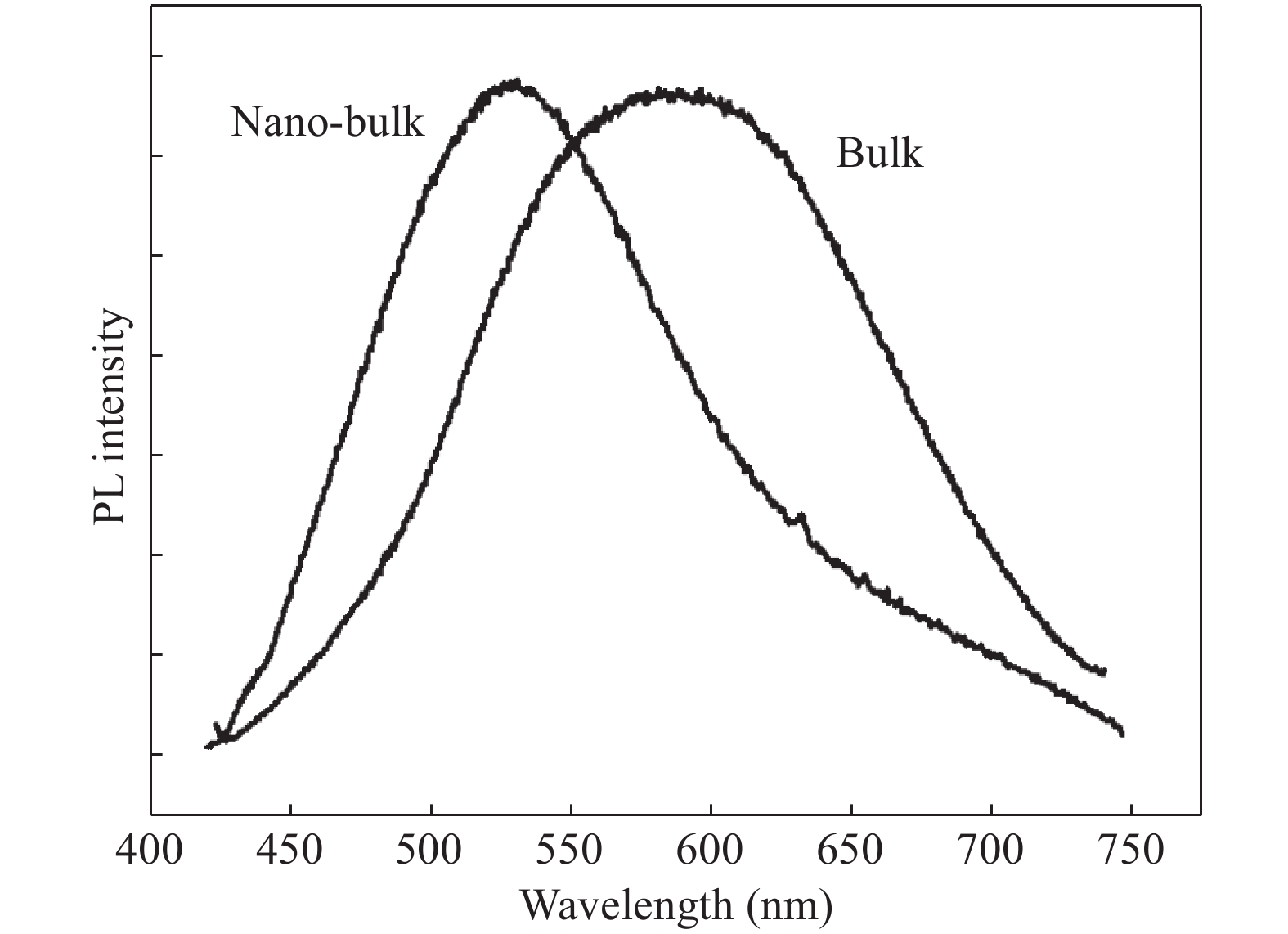
Abstract: Nano-particles of cadmium sulphide were deposited on cleaned copper substrate by an automated sequential ionic layer adsorption reaction (SILAR) system. The grown nano-bulk junction exhibits Schottky diode behavior. The response of the nano-bulk junction was investigated under oxygen and hydrogen atmospheric conditions. The gas response ratio was found to be 198% for Oxygen and 34% for Hydrogen at room temperature. An increase in the operating temperature of the nano-bulk junction resulted in a decrease in their gas response ratio. A logarithmic dependence on the oxygen partial pressure to the junction response was observed, indicating a Temkin isothermal behavior. Work function measurements using a Kelvin probe demonstrate that the exposure to an oxygen atmosphere fails to effectively separate the charges due to the built-in electric field at the interface. Based on the benefits like simple structure, ease of fabrication and response ratio the studied device is a promising candidate for gas detection applications.
Key words: Cu/CdS; nano-bulk junction, hydrogen, work function, gas response ratio
| [1] |
Azulay D, Millo O, Silbert S, et al. Where does photocurrent flow in polycrystalline CdS. Appl Phys Lett, 2005, 86: 212102 doi: 10.1063/1.1923157
|
| [2] |
Grus M, Sikorska A. Characterization of the absorption edge in crystalline CdS:Cu powder by use of photoacoustic and reflection spectroscopy. Physica B, 1999, 266: 139 doi: 10.1016/S0921-4526(98)01290-3
|
| [3] |
Rakhshani A E. Study of Urbach tail, bandgap energy and grain-boundary characteristics in CdS by modulated photocurrent spectroscopy. J Phys: Condens Matter, 2000, 12: 4391 doi: 10.1088/0953-8984/12/19/309
|
| [4] |
Kokaj J, Rakhshani A E. CdS thin film transistor for inverter and operational amplifier circuit. J Phys D, 2004, 37: 1970 doi: 10.1088/0022-3727/37/14/012
|
| [5] |
Kadam A N, Dhabbe R S, Kokate M R, et al. Room temperature synthesis of CdS nanoflakes for photocatalytic properties. J Mater Sci: Mater Electron, 2014, 25: 1887 doi: 10.1007/s10854-014-1816-3
|
| [6] |
Jayakrishnan R. Negative resistance in Cu2O/In2S3 heterostructure. Mater Chem Phys, 2015, 162: 542 doi: 10.1016/j.matchemphys.2015.06.025
|
| [7] |
Giberti A, Gaiardo A, Fabbri B, et al. Metal sulfides as sensing materials for chemoresistive gas sensors. Sens Actuators B, 2016, 223: 827 doi: 10.1016/j.snb.2015.10.007
|
| [8] |
Kim S, Park S, Park S, et al. Acetone sensing of Au and Pd-decorated WO3 nanorod sensors. Sens Actuators B, 2015, 209: 180 doi: 10.1016/j.snb.2014.11.106
|
| [9] |
Dumbrava A, Badea C, Prodan G, et al. Zinc sulphide fine particles obtained at low temperature. Chalcogenide Lett, 2009, 6: 437
|
| [10] |
Wang Y, Herron N. Nanometer-sized semiconductor clusters: materials synthesis, quantum size effects, and photophysical properties. J Phys Chem, 1991, 95: 525 doi: 10.1021/j100155a009
|
| [11] |
Eranna G, Joshi B C, Runthala D P, et al. Oxide materials for development of integrated gas sensors—a comprehensive review. Crit Rev Solid State Mater Sci, 2004, 29: 111 doi: 10.1080/10408430490888977
|
| [12] |
Jayakrishnan R, Kurian A S, Nair V G, et al. Effect of vacuum annealing on the photoconductivity of CuO thin films grown using sequential ionic layer adsorption reaction. Mater Chem Phys, 2016, 180: 149 doi: 10.1016/j.matchemphys.2016.05.055
|
| [13] |
Shafiei M, Sadek A, Yu J, et al. Pt/WO3 nanoplatelet/SiC Schottky diode based hydrogen gas sensor. Sens Lett, 2011, 9: 11 doi: 10.1166/sl.2011.1409
|
| [14] |
Hu Y, Zhou X, Han Q, et al. Sensing properties of CuO–ZnO heterojunction gas sensors. Mater Sci Eng B, 2003, 99: 41 doi: 10.1016/S0921-5107(02)00446-4
|
| [15] |
Yoon D H, Yu J H, Choi G M. CO gas sensing properties of ZnO–CuO composite. Sens Actuator B, 1998, 46: 15 doi: 10.1016/S0925-4005(97)00317-1
|
| [16] |
Zhu C L, Chen Y J, Wang R X, et al. SnO2 surfactant composite films for superior gas sensitivity. Sens Actuator B, 2009, 140: 185 doi: 10.1016/j.snb.2009.04.011
|
| [17] |
Fergus J W. Perovskite oxides for semiconductor-based gas sensors. Sens Actuator B, 2007, 123: 1169 doi: 10.1016/j.snb.2006.10.051
|
| [18] |
Korotcenkov G. Metal oxides for solid-state gas sensors: what determines our choice. Mater Sci Eng B, 2007, 139: 1 doi: 10.1016/j.mseb.2007.01.044
|
| [19] |
Barsan N, Schweizer-Berberich M, Fresenius G W. Fundamental and practical aspects in the design of nanoscaled SnO2 gas sensors: a status report. J Anal Chem, 1999, 365: 287 doi: 10.1007/s002160051490
|
| [20] |
Chopra K L. Thin film phenomena. New York: MC Graw Hill Co., 1969
|
| [21] |
Weaver J M R, Abraham D W. High resolution atomic force microscopy potentiometry. J Vac Sci Technol B, 1991, 9: 1559 doi: 10.1116/1.585423
|
| [22] |
Nonnenmacher M, O’Boyle M P, Wickeramasinghe H K. Kelvin probe force microscopy. Appl Phys Lett, 1991, 58: 2921 doi: 10.1063/1.105227
|
| [23] |
Scherrer P. Bestimmung der Gr??e und der inneren Struktur von Kolloidteilchen mittels R?ntgenstrahlen. Mathematisch-Physikalische Klasse, 1918, 2: 98
|
| [24] |
Rau U, Schock H W. Electronic properties of Cu(In,Ga)Se2 heterojunction solar cells—recent achievements, current understanding, and future challenges. Appl Phys A, 1999, 69: 131 doi: 10.1007/s003390050984
|
| [25] |
Clark V A. The theory of adsorption and catalysis. New York: Academic, 1970
|
| [26] |
Rhoderick E. Metal–semiconductor contacts. IEE Proc I, 1982, 129: 1
|
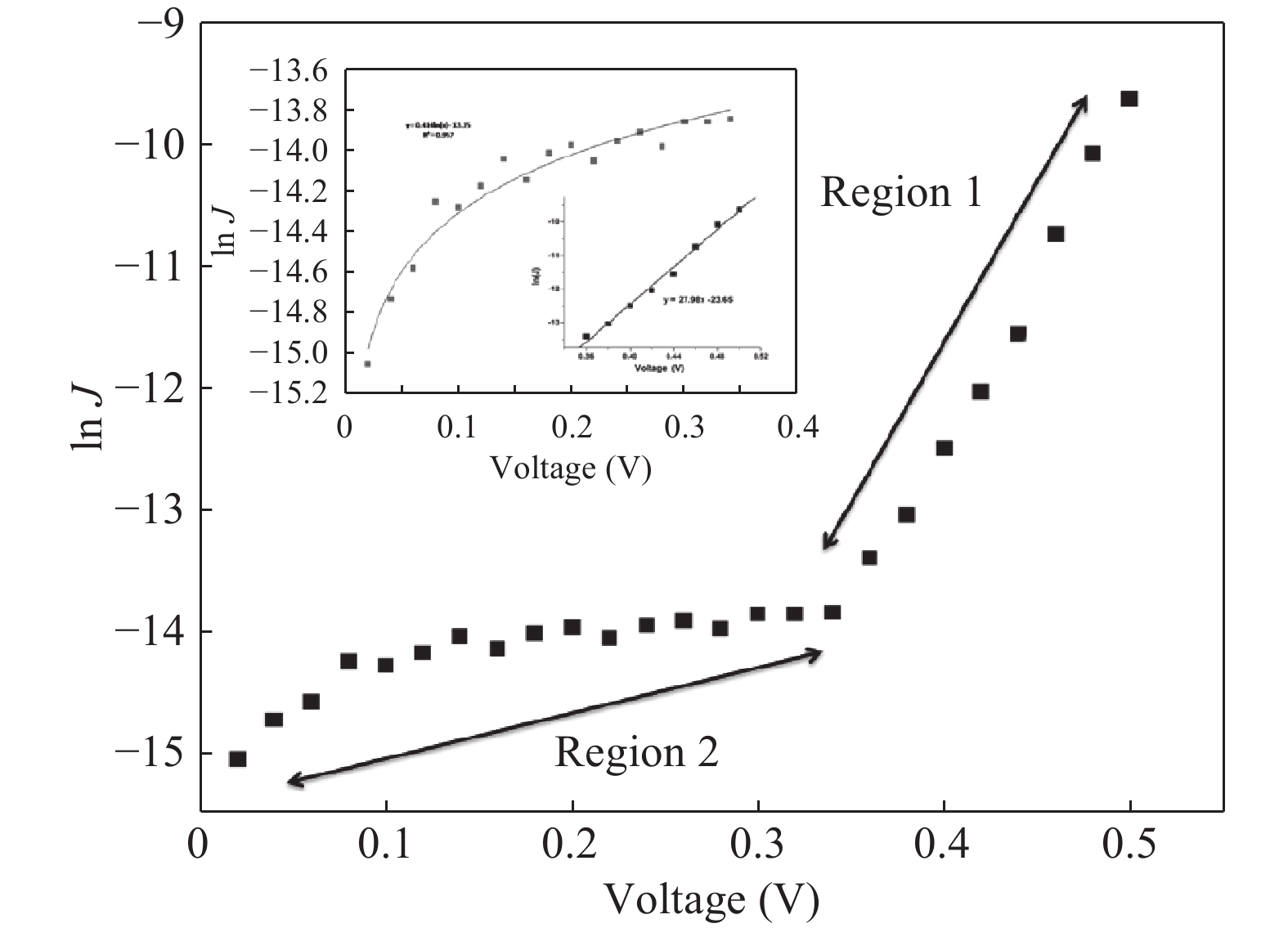
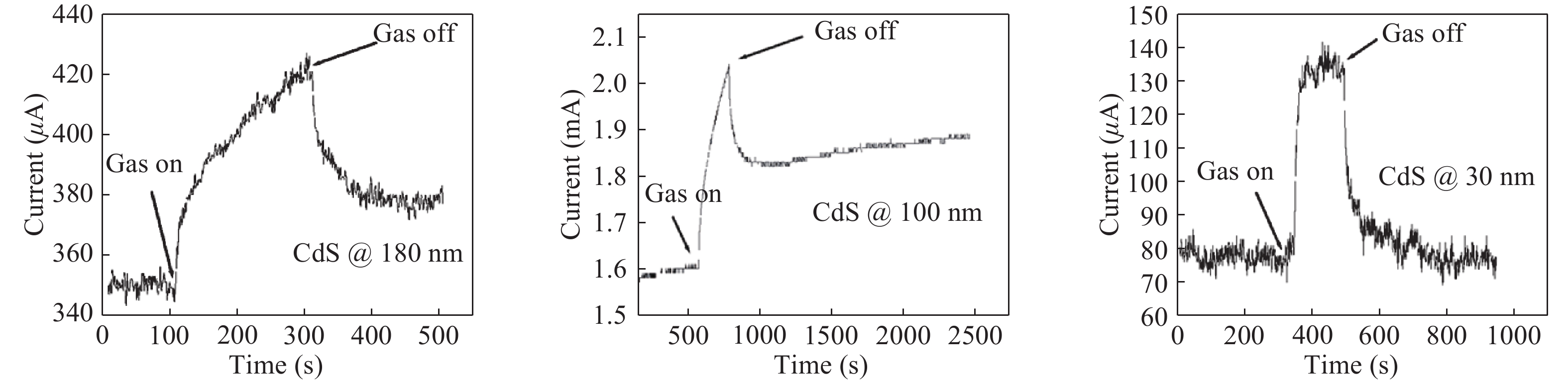
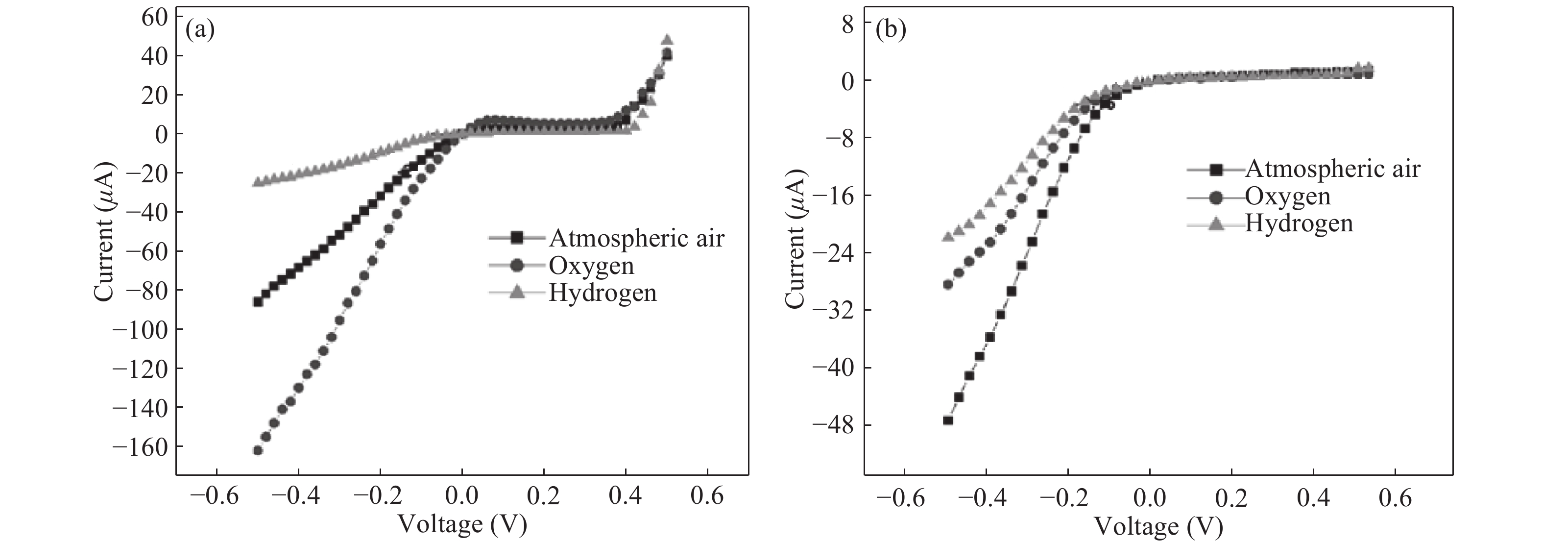
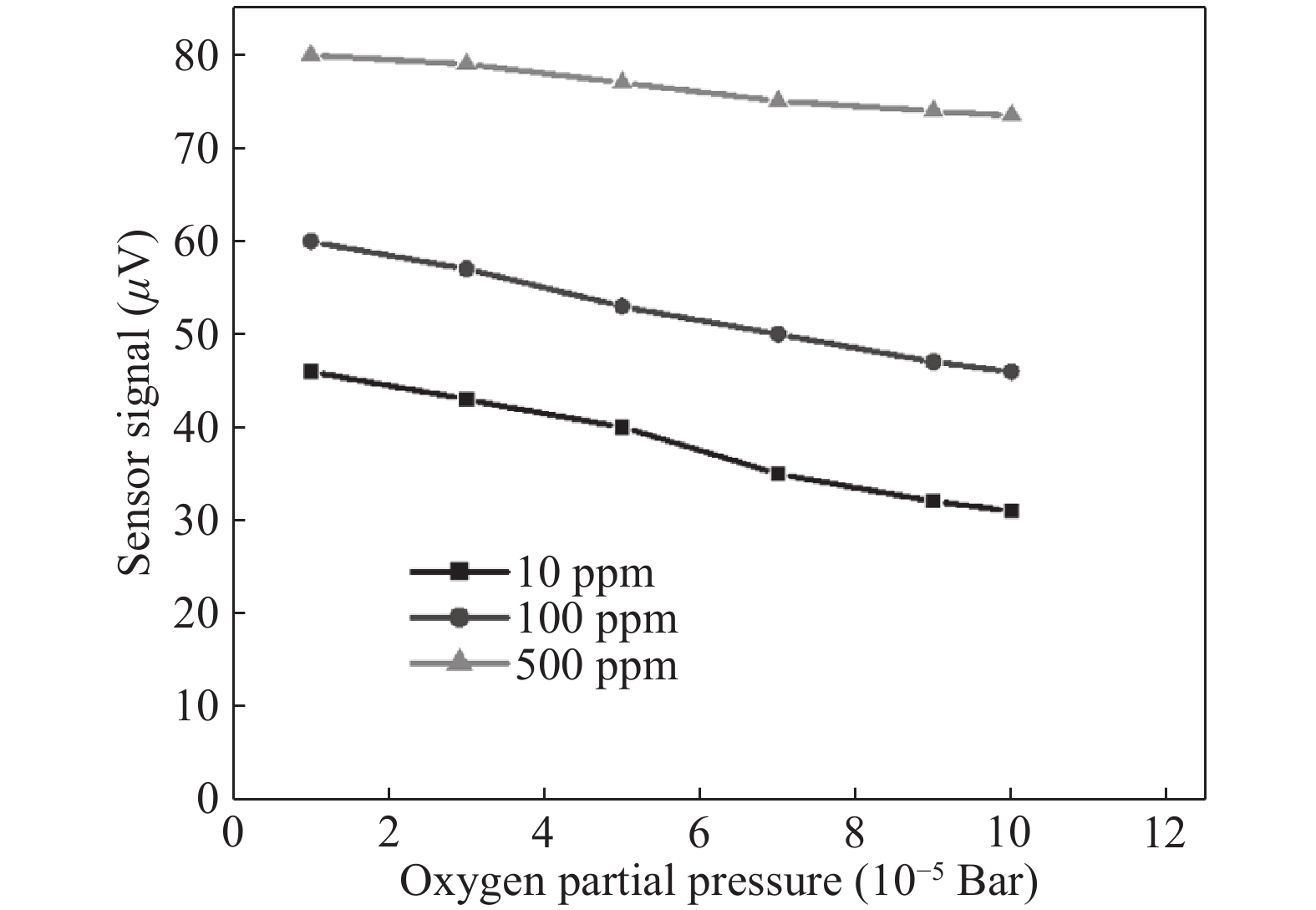
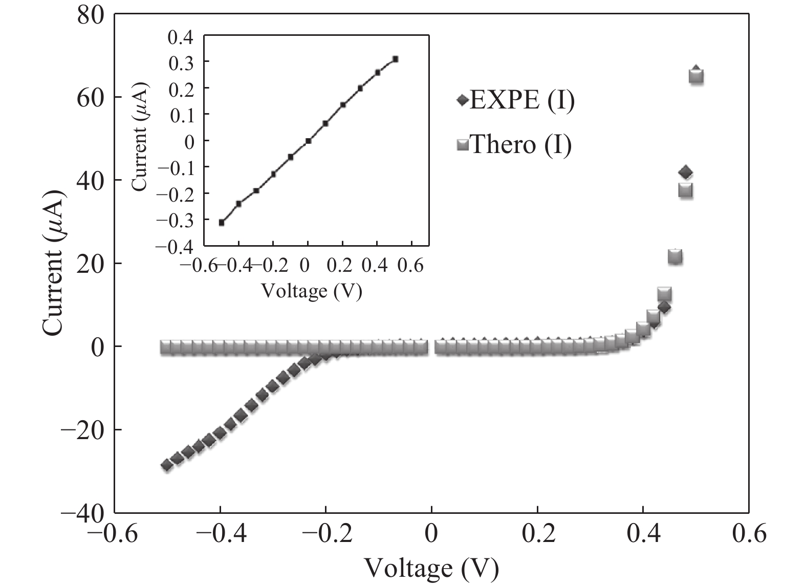
Table 1. Surface potential and work function measured for the nano-bulk junction before and after soaking in oxygen inside a gas chamber.
| Sample | Surface
potential |
Work function calibrated with Au | Surface potential after
soaking in Oxygen |
Work function after
soaking in oxygen calibrated with Au |
||
| (mV) | (eV) | (mV) | (eV) | |||
| Cu substrate | ?145 ± 4 | 5.105 | ||||
| Cu/CdS | ?575 ± 5 | 4.675 | ?544 ± 8 | 4.706 | ||
| Annealed Cu/CdS | ?584 ± 5 | 4.656 | ?584 ± 3 | 4666 |
 DownLoad: CSV
| [1] |
Azulay D, Millo O, Silbert S, et al. Where does photocurrent flow in polycrystalline CdS. Appl Phys Lett, 2005, 86: 212102 doi: 10.1063/1.1923157
|
| [2] |
Grus M, Sikorska A. Characterization of the absorption edge in crystalline CdS:Cu powder by use of photoacoustic and reflection spectroscopy. Physica B, 1999, 266: 139 doi: 10.1016/S0921-4526(98)01290-3
|
| [3] |
Rakhshani A E. Study of Urbach tail, bandgap energy and grain-boundary characteristics in CdS by modulated photocurrent spectroscopy. J Phys: Condens Matter, 2000, 12: 4391 doi: 10.1088/0953-8984/12/19/309
|
| [4] |
Kokaj J, Rakhshani A E. CdS thin film transistor for inverter and operational amplifier circuit. J Phys D, 2004, 37: 1970 doi: 10.1088/0022-3727/37/14/012
|
| [5] |
Kadam A N, Dhabbe R S, Kokate M R, et al. Room temperature synthesis of CdS nanoflakes for photocatalytic properties. J Mater Sci: Mater Electron, 2014, 25: 1887 doi: 10.1007/s10854-014-1816-3
|
| [6] |
Jayakrishnan R. Negative resistance in Cu2O/In2S3 heterostructure. Mater Chem Phys, 2015, 162: 542 doi: 10.1016/j.matchemphys.2015.06.025
|
| [7] |
Giberti A, Gaiardo A, Fabbri B, et al. Metal sulfides as sensing materials for chemoresistive gas sensors. Sens Actuators B, 2016, 223: 827 doi: 10.1016/j.snb.2015.10.007
|
| [8] |
Kim S, Park S, Park S, et al. Acetone sensing of Au and Pd-decorated WO3 nanorod sensors. Sens Actuators B, 2015, 209: 180 doi: 10.1016/j.snb.2014.11.106
|
| [9] |
Dumbrava A, Badea C, Prodan G, et al. Zinc sulphide fine particles obtained at low temperature. Chalcogenide Lett, 2009, 6: 437
|
| [10] |
Wang Y, Herron N. Nanometer-sized semiconductor clusters: materials synthesis, quantum size effects, and photophysical properties. J Phys Chem, 1991, 95: 525 doi: 10.1021/j100155a009
|
| [11] |
Eranna G, Joshi B C, Runthala D P, et al. Oxide materials for development of integrated gas sensors—a comprehensive review. Crit Rev Solid State Mater Sci, 2004, 29: 111 doi: 10.1080/10408430490888977
|
| [12] |
Jayakrishnan R, Kurian A S, Nair V G, et al. Effect of vacuum annealing on the photoconductivity of CuO thin films grown using sequential ionic layer adsorption reaction. Mater Chem Phys, 2016, 180: 149 doi: 10.1016/j.matchemphys.2016.05.055
|
| [13] |
Shafiei M, Sadek A, Yu J, et al. Pt/WO3 nanoplatelet/SiC Schottky diode based hydrogen gas sensor. Sens Lett, 2011, 9: 11 doi: 10.1166/sl.2011.1409
|
| [14] |
Hu Y, Zhou X, Han Q, et al. Sensing properties of CuO–ZnO heterojunction gas sensors. Mater Sci Eng B, 2003, 99: 41 doi: 10.1016/S0921-5107(02)00446-4
|
| [15] |
Yoon D H, Yu J H, Choi G M. CO gas sensing properties of ZnO–CuO composite. Sens Actuator B, 1998, 46: 15 doi: 10.1016/S0925-4005(97)00317-1
|
| [16] |
Zhu C L, Chen Y J, Wang R X, et al. SnO2 surfactant composite films for superior gas sensitivity. Sens Actuator B, 2009, 140: 185 doi: 10.1016/j.snb.2009.04.011
|
| [17] |
Fergus J W. Perovskite oxides for semiconductor-based gas sensors. Sens Actuator B, 2007, 123: 1169 doi: 10.1016/j.snb.2006.10.051
|
| [18] |
Korotcenkov G. Metal oxides for solid-state gas sensors: what determines our choice. Mater Sci Eng B, 2007, 139: 1 doi: 10.1016/j.mseb.2007.01.044
|
| [19] |
Barsan N, Schweizer-Berberich M, Fresenius G W. Fundamental and practical aspects in the design of nanoscaled SnO2 gas sensors: a status report. J Anal Chem, 1999, 365: 287 doi: 10.1007/s002160051490
|
| [20] |
Chopra K L. Thin film phenomena. New York: MC Graw Hill Co., 1969
|
| [21] |
Weaver J M R, Abraham D W. High resolution atomic force microscopy potentiometry. J Vac Sci Technol B, 1991, 9: 1559 doi: 10.1116/1.585423
|
| [22] |
Nonnenmacher M, O’Boyle M P, Wickeramasinghe H K. Kelvin probe force microscopy. Appl Phys Lett, 1991, 58: 2921 doi: 10.1063/1.105227
|
| [23] |
Scherrer P. Bestimmung der Gr??e und der inneren Struktur von Kolloidteilchen mittels R?ntgenstrahlen. Mathematisch-Physikalische Klasse, 1918, 2: 98
|
| [24] |
Rau U, Schock H W. Electronic properties of Cu(In,Ga)Se2 heterojunction solar cells—recent achievements, current understanding, and future challenges. Appl Phys A, 1999, 69: 131 doi: 10.1007/s003390050984
|
| [25] |
Clark V A. The theory of adsorption and catalysis. New York: Academic, 1970
|
| [26] |
Rhoderick E. Metal–semiconductor contacts. IEE Proc I, 1982, 129: 1
|


Article views: 3853 Times PDF downloads: 33 Times Cited by: 0 Times
Received: 28 March 2017 Revised: 12 July 2017 Online: Uncorrected proof: 24 January 2018Published: 01 March 2018
| Citation: |
R. Jayakrishnan, Varun G Nair, Akhil M Anand, Meera Venugopal. Gas selectivity of SILAR grown CdS nano-bulk junction[J]. Journal of Semiconductors, 2018, 39(3): 033002. doi: 10.1088/1674-4926/39/3/033002
****
R Jayakrishnan, V G Nair, A M Anand, M Venugopal, Gas selectivity of SILAR grown CdS nano-bulk junction[J]. J. Semicond., 2018, 39(3): 033002. doi: 10.1088/1674-4926/39/3/033002.

|
| [1] |
Azulay D, Millo O, Silbert S, et al. Where does photocurrent flow in polycrystalline CdS. Appl Phys Lett, 2005, 86: 212102 doi: 10.1063/1.1923157
|
| [2] |
Grus M, Sikorska A. Characterization of the absorption edge in crystalline CdS:Cu powder by use of photoacoustic and reflection spectroscopy. Physica B, 1999, 266: 139 doi: 10.1016/S0921-4526(98)01290-3
|
| [3] |
Rakhshani A E. Study of Urbach tail, bandgap energy and grain-boundary characteristics in CdS by modulated photocurrent spectroscopy. J Phys: Condens Matter, 2000, 12: 4391 doi: 10.1088/0953-8984/12/19/309
|
| [4] |
Kokaj J, Rakhshani A E. CdS thin film transistor for inverter and operational amplifier circuit. J Phys D, 2004, 37: 1970 doi: 10.1088/0022-3727/37/14/012
|
| [5] |
Kadam A N, Dhabbe R S, Kokate M R, et al. Room temperature synthesis of CdS nanoflakes for photocatalytic properties. J Mater Sci: Mater Electron, 2014, 25: 1887 doi: 10.1007/s10854-014-1816-3
|
| [6] |
Jayakrishnan R. Negative resistance in Cu2O/In2S3 heterostructure. Mater Chem Phys, 2015, 162: 542 doi: 10.1016/j.matchemphys.2015.06.025
|
| [7] |
Giberti A, Gaiardo A, Fabbri B, et al. Metal sulfides as sensing materials for chemoresistive gas sensors. Sens Actuators B, 2016, 223: 827 doi: 10.1016/j.snb.2015.10.007
|
| [8] |
Kim S, Park S, Park S, et al. Acetone sensing of Au and Pd-decorated WO3 nanorod sensors. Sens Actuators B, 2015, 209: 180 doi: 10.1016/j.snb.2014.11.106
|
| [9] |
Dumbrava A, Badea C, Prodan G, et al. Zinc sulphide fine particles obtained at low temperature. Chalcogenide Lett, 2009, 6: 437
|
| [10] |
Wang Y, Herron N. Nanometer-sized semiconductor clusters: materials synthesis, quantum size effects, and photophysical properties. J Phys Chem, 1991, 95: 525 doi: 10.1021/j100155a009
|
| [11] |
Eranna G, Joshi B C, Runthala D P, et al. Oxide materials for development of integrated gas sensors—a comprehensive review. Crit Rev Solid State Mater Sci, 2004, 29: 111 doi: 10.1080/10408430490888977
|
| [12] |
Jayakrishnan R, Kurian A S, Nair V G, et al. Effect of vacuum annealing on the photoconductivity of CuO thin films grown using sequential ionic layer adsorption reaction. Mater Chem Phys, 2016, 180: 149 doi: 10.1016/j.matchemphys.2016.05.055
|
| [13] |
Shafiei M, Sadek A, Yu J, et al. Pt/WO3 nanoplatelet/SiC Schottky diode based hydrogen gas sensor. Sens Lett, 2011, 9: 11 doi: 10.1166/sl.2011.1409
|
| [14] |
Hu Y, Zhou X, Han Q, et al. Sensing properties of CuO–ZnO heterojunction gas sensors. Mater Sci Eng B, 2003, 99: 41 doi: 10.1016/S0921-5107(02)00446-4
|
| [15] |
Yoon D H, Yu J H, Choi G M. CO gas sensing properties of ZnO–CuO composite. Sens Actuator B, 1998, 46: 15 doi: 10.1016/S0925-4005(97)00317-1
|
| [16] |
Zhu C L, Chen Y J, Wang R X, et al. SnO2 surfactant composite films for superior gas sensitivity. Sens Actuator B, 2009, 140: 185 doi: 10.1016/j.snb.2009.04.011
|
| [17] |
Fergus J W. Perovskite oxides for semiconductor-based gas sensors. Sens Actuator B, 2007, 123: 1169 doi: 10.1016/j.snb.2006.10.051
|
| [18] |
Korotcenkov G. Metal oxides for solid-state gas sensors: what determines our choice. Mater Sci Eng B, 2007, 139: 1 doi: 10.1016/j.mseb.2007.01.044
|
| [19] |
Barsan N, Schweizer-Berberich M, Fresenius G W. Fundamental and practical aspects in the design of nanoscaled SnO2 gas sensors: a status report. J Anal Chem, 1999, 365: 287 doi: 10.1007/s002160051490
|
| [20] |
Chopra K L. Thin film phenomena. New York: MC Graw Hill Co., 1969
|
| [21] |
Weaver J M R, Abraham D W. High resolution atomic force microscopy potentiometry. J Vac Sci Technol B, 1991, 9: 1559 doi: 10.1116/1.585423
|
| [22] |
Nonnenmacher M, O’Boyle M P, Wickeramasinghe H K. Kelvin probe force microscopy. Appl Phys Lett, 1991, 58: 2921 doi: 10.1063/1.105227
|
| [23] |
Scherrer P. Bestimmung der Gr??e und der inneren Struktur von Kolloidteilchen mittels R?ntgenstrahlen. Mathematisch-Physikalische Klasse, 1918, 2: 98
|
| [24] |
Rau U, Schock H W. Electronic properties of Cu(In,Ga)Se2 heterojunction solar cells—recent achievements, current understanding, and future challenges. Appl Phys A, 1999, 69: 131 doi: 10.1007/s003390050984
|
| [25] |
Clark V A. The theory of adsorption and catalysis. New York: Academic, 1970
|
| [26] |
Rhoderick E. Metal–semiconductor contacts. IEE Proc I, 1982, 129: 1
|

 WeChat ID
Journal of Semiconductors © 2017 All Rights Reserved 京ICP備05085259號(hào)-2