


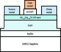
Fig. 1.
(Color online) Schematic cross section of AlGaN/GaN HEMTs with selective area grown (SAG) p-GaN gates.
SEMICONDUCTOR DEVICES
Yuliang Huang, Lian Zhang, Zhe Cheng, Yun Zhang, Yujie Ai, Yongbing Zhao, Hongxi Lu, Junxi Wang and Jinmin Li
Corresponding author: Zhang Yun,yzhang34@semi.ac.cn
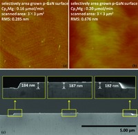
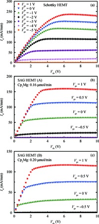
Abstract: We report a selective area growth (SAG) method to define the p-GaN gate of AlGaN/GaN high electron mobility transistors (HEMTs) by metal-organic chemical vapor deposition. Compared with Schottky gate HEMTs, the SAG p-GaN gate HEMTs show more positive threshold voltage (Vth) and better gate control ability. The influence of Cp2Mg flux of SAG p-GaN gate on the AlGaN/GaN HEMTs has also been studied. With the increasing Cp2Mg from 0.16 μmol/min to 0.20 μmol/min, the Vth raises from -67 V to -37 V. The maximum transconductance of the SAG HEMT at a drain voltage of 10 V is 113.9 mS/mm while that value of the Schottky HEMT is 51.6 mS/mm. The SAG method paves a promising way for achieving p-GaN gate normally-off AlGaN/GaN HEMTs without dry etching damage.
Key words: AlGaN/GaN, selective area growth, normally off, HEMT
| [1] |
Ambacher O, Foutz B, Smart J, et al. Two dimensional electron gases induced by spontaneous and piezoelectric polarization in undoped and doped AlGaN/GaN heterostructures. J Appl Phys, 2000, 87(1):334 doi: 10.1063/1.371866
|
| [2] |
Tan Xin, Lü Yuanjie, Gu Guodong, et al. High performance AlGaN/GaN HEMTs with AlN/SiNx passivation. Journal of Semiconductors, 2015, 36(7):074008 doi: 10.1088/1674-4926/36/7/074008
|
| [3] |
Khan M A, Chen Q, Sun C J, et al. Enhancement and depletion mode GaN/AlGaN heterostructure field effect transistors. Appl Phys Lett, 1996, 68(4):514 doi: 10.1063/1.116384
|
| [4] |
Wang Zheli, Zhou Jianjun, Kong Yuechan, et al. Thin-barrier enhancement-mode AlGaN/GaN MIS-HEMT using ALD Al2O3 as gate insulator. Journal of Semiconductors, 2015, 36(9):094004 doi: 10.1088/1674-4926/36/9/094004
|
| [5] |
Cai Y, Zhou Y G, Lau K M, et al. Control of threshold voltage of AlGaN/GaN HEMTs by fluoride-based plasma treatment:from depletion mode to enhancement mode. IEEE Trans Electron Devices, 2006, 53(9):2207 doi: 10.1109/TED.2006.881054
|
| [6] |
Su L Y, Lee F, Huang J J. Enhancement-mode GaN-based highelectron mobility transistors on the Si substrate with a p-type GaN cap layer. IEEE Trans Electron Devices, 2014, 61(2):460 doi: 10.1109/TED.2013.2294337
|
| [7] |
Hwang I, Choi H, Lee J, et al. 1.6 kV, 2.9 mΩ·cm2 normally-off p-GaN HEMT device. Proceedings of the 201224th International Symposium on Power Semiconductor Devices and ICs, 2012:41
|
| [8] |
Hwang I, Kim J, Choi H S, et al. p-GaN gate HEMTs with tungsten gate metal for high threshold voltage and low gate current. IEEE Electron Device Lett, 2013, 34(2):202 doi: 10.1109/LED.2012.2230312
|
| [9] |
Deguchi T, Kikuchi T, Arai M, et al. High on/off current ratio pInGaN/AlGaN/GaN HEMTs. IEEE Electron Device Lett, 2012,33(9):1249 doi: 10.1109/LED.2012.2204854
|
| [10] |
Hilt O, Brunner F, Cho E, et al. Normally-off high-voltage p-GaN gate GaN HFET with carbon-doped buffer. Proceedings of the 23rd International Symposium on Power Semiconductor Devices & IC's, 2011:239
|
| [11] |
Mizutani T, Yamada H, Kishimoto S, et al. Normally off AlGaN/GaN high electron mobility transistors with p-InGaN cap layer. J Appl Phys, 2013, 113(3):034502 doi: 10.1063/1.4775494
|
| [12] |
Lanford W B, Tanaka T, Otoki Y, et al. Recessed-gate enhancement-mode GaN HEMT with high threshold voltage. Electron Lett, 2005, 41(7):449 doi: 10.1049/el:20050161
|
| [13] |
Wakejima A, Ando A, Watanabe A, et al. Normally off AlGaN/GaN HEMT on Si substrate with selectively dry-etched recessed gate and polarization-charge-compensation ?-doped GaN cap layer. Appl Phys Express, 2015, 8(2):026502 doi: 10.7567/APEX.8.026502
|
| [14] |
Lee Y C, Wang C Y, Kao T T, et al. Threshold voltage control of recessed-gate Ⅲ-N HFETs using an electrode-less wet etching technique. CS MANTECH Conference, 2012
|
| [15] |
Yao Y, He Z Y, Yang F, et al. Normally-off GaN recessed-gate MOSFET fabricated by selective area growth technique. Appl Phys Express, 2014, 7(1):016502 doi: 10.7567/APEX.7.016502
|
| [16] |
Lee Y C, Kao T T, Merola J J, et al. A remote-oxygen-plasma surface treatment technique for Ⅲ-nitride heterojunction fieldeffect transistors. IEEE Trans Electron Devices, 2014, 61(2):493 doi: 10.1109/TED.2013.2295828
|
| [17] |
Tsuyukuchi N, Nagamarsu K, Hirosi Y, et al. Low-leakagecurrent enhancement-mode AlGaN/GaN heterostructure fieldeffect transistor using p-type gate contact. Jpn J Appl Phys, Part 2, 2006, 45(8-11):L319 doi: 10.1143/JJAP.45.L319/pdf
|
| [18] |
Fujii T, Tsuyukuchi N, Hirose Y, et al. Fabrication of enhancement-mode AlxGa1-xN/GaN junction heterostructure field-effect transistors with p-type GaN gate contact. Physica Status Solidi (c), 2007, 4(7):2708 doi: 10.1002/(ISSN)1610-1642
|
| [19] |
Fujii T, Tsuyukuchi N, Iwaya M, et al. High on/off ratio in enhancement-mode AlxGa1-xN/GaN junction heterostructure field-effect transistors with p-type GaN gate contact. Jpn J Appl Phys, 2006, 45(37-41):L1048 http://cn.bing.com/academic/profile?id=1989037470&encoded=0&v=paper_preview&mkt=zh-cn
|
| [20] |
Hao Y. Nitride wide band gap semiconductor materials and electronic devices. Beijing:Science Press, 2013
|
| [21] |
Uemoto Y, Hikita M, Ueno H, et al. Gate injection transistor (GIT)-a normally-off AlGaN/GaN power transistor using conductivity modulation. IEEE Trans Electron Devices, 2007, 54(12):3393 doi: 10.1109/TED.2007.908601
|


Article views: 4554 Times PDF downloads: 156 Times Cited by: 0 Times
Received: 06 May 2016 Revised: 24 May 2016 Online: Published: 01 November 2016
| Citation: |
Yuliang Huang, Lian Zhang, Zhe Cheng, Yun Zhang, Yujie Ai, Yongbing Zhao, Hongxi Lu, Junxi Wang, Jinmin Li. AlGaN/GaN high electron mobility transistors with selective area grown p-GaN gates[J]. Journal of Semiconductors, 2016, 37(11): 114002. doi: 10.1088/1674-4926/37/11/114002
****
Y L Huang, L Zhang, Z Cheng, Y Zhang, Y J Ai, Y B Zhao, H X Lu, J X Wang, J M Li. AlGaN/GaN high electron mobility transistors with selective area grown p-GaN gates[J]. J. Semicond., 2016, 37(11): 114002. doi: 10.1088/1674-4926/37/11/114002.

|
National High Technology Program of China No. 2014AA032606
National Natural Sciences Foundation of China Nos. 61376090, 61306008
Project supported by the National Natural Sciences Foundation of China (Nos. 61376090, 61306008) and the National High Technology Program of China (No. 2014AA032606).
| [1] |
Ambacher O, Foutz B, Smart J, et al. Two dimensional electron gases induced by spontaneous and piezoelectric polarization in undoped and doped AlGaN/GaN heterostructures. J Appl Phys, 2000, 87(1):334 doi: 10.1063/1.371866
|
| [2] |
Tan Xin, Lü Yuanjie, Gu Guodong, et al. High performance AlGaN/GaN HEMTs with AlN/SiNx passivation. Journal of Semiconductors, 2015, 36(7):074008 doi: 10.1088/1674-4926/36/7/074008
|
| [3] |
Khan M A, Chen Q, Sun C J, et al. Enhancement and depletion mode GaN/AlGaN heterostructure field effect transistors. Appl Phys Lett, 1996, 68(4):514 doi: 10.1063/1.116384
|
| [4] |
Wang Zheli, Zhou Jianjun, Kong Yuechan, et al. Thin-barrier enhancement-mode AlGaN/GaN MIS-HEMT using ALD Al2O3 as gate insulator. Journal of Semiconductors, 2015, 36(9):094004 doi: 10.1088/1674-4926/36/9/094004
|
| [5] |
Cai Y, Zhou Y G, Lau K M, et al. Control of threshold voltage of AlGaN/GaN HEMTs by fluoride-based plasma treatment:from depletion mode to enhancement mode. IEEE Trans Electron Devices, 2006, 53(9):2207 doi: 10.1109/TED.2006.881054
|
| [6] |
Su L Y, Lee F, Huang J J. Enhancement-mode GaN-based highelectron mobility transistors on the Si substrate with a p-type GaN cap layer. IEEE Trans Electron Devices, 2014, 61(2):460 doi: 10.1109/TED.2013.2294337
|
| [7] |
Hwang I, Choi H, Lee J, et al. 1.6 kV, 2.9 mΩ·cm2 normally-off p-GaN HEMT device. Proceedings of the 201224th International Symposium on Power Semiconductor Devices and ICs, 2012:41
|
| [8] |
Hwang I, Kim J, Choi H S, et al. p-GaN gate HEMTs with tungsten gate metal for high threshold voltage and low gate current. IEEE Electron Device Lett, 2013, 34(2):202 doi: 10.1109/LED.2012.2230312
|
| [9] |
Deguchi T, Kikuchi T, Arai M, et al. High on/off current ratio pInGaN/AlGaN/GaN HEMTs. IEEE Electron Device Lett, 2012,33(9):1249 doi: 10.1109/LED.2012.2204854
|
| [10] |
Hilt O, Brunner F, Cho E, et al. Normally-off high-voltage p-GaN gate GaN HFET with carbon-doped buffer. Proceedings of the 23rd International Symposium on Power Semiconductor Devices & IC's, 2011:239
|
| [11] |
Mizutani T, Yamada H, Kishimoto S, et al. Normally off AlGaN/GaN high electron mobility transistors with p-InGaN cap layer. J Appl Phys, 2013, 113(3):034502 doi: 10.1063/1.4775494
|
| [12] |
Lanford W B, Tanaka T, Otoki Y, et al. Recessed-gate enhancement-mode GaN HEMT with high threshold voltage. Electron Lett, 2005, 41(7):449 doi: 10.1049/el:20050161
|
| [13] |
Wakejima A, Ando A, Watanabe A, et al. Normally off AlGaN/GaN HEMT on Si substrate with selectively dry-etched recessed gate and polarization-charge-compensation ?-doped GaN cap layer. Appl Phys Express, 2015, 8(2):026502 doi: 10.7567/APEX.8.026502
|
| [14] |
Lee Y C, Wang C Y, Kao T T, et al. Threshold voltage control of recessed-gate Ⅲ-N HFETs using an electrode-less wet etching technique. CS MANTECH Conference, 2012
|
| [15] |
Yao Y, He Z Y, Yang F, et al. Normally-off GaN recessed-gate MOSFET fabricated by selective area growth technique. Appl Phys Express, 2014, 7(1):016502 doi: 10.7567/APEX.7.016502
|
| [16] |
Lee Y C, Kao T T, Merola J J, et al. A remote-oxygen-plasma surface treatment technique for Ⅲ-nitride heterojunction fieldeffect transistors. IEEE Trans Electron Devices, 2014, 61(2):493 doi: 10.1109/TED.2013.2295828
|
| [17] |
Tsuyukuchi N, Nagamarsu K, Hirosi Y, et al. Low-leakagecurrent enhancement-mode AlGaN/GaN heterostructure fieldeffect transistor using p-type gate contact. Jpn J Appl Phys, Part 2, 2006, 45(8-11):L319 doi: 10.1143/JJAP.45.L319/pdf
|
| [18] |
Fujii T, Tsuyukuchi N, Hirose Y, et al. Fabrication of enhancement-mode AlxGa1-xN/GaN junction heterostructure field-effect transistors with p-type GaN gate contact. Physica Status Solidi (c), 2007, 4(7):2708 doi: 10.1002/(ISSN)1610-1642
|
| [19] |
Fujii T, Tsuyukuchi N, Iwaya M, et al. High on/off ratio in enhancement-mode AlxGa1-xN/GaN junction heterostructure field-effect transistors with p-type GaN gate contact. Jpn J Appl Phys, 2006, 45(37-41):L1048 http://cn.bing.com/academic/profile?id=1989037470&encoded=0&v=paper_preview&mkt=zh-cn
|
| [20] |
Hao Y. Nitride wide band gap semiconductor materials and electronic devices. Beijing:Science Press, 2013
|
| [21] |
Uemoto Y, Hikita M, Ueno H, et al. Gate injection transistor (GIT)-a normally-off AlGaN/GaN power transistor using conductivity modulation. IEEE Trans Electron Devices, 2007, 54(12):3393 doi: 10.1109/TED.2007.908601
|

 WeChat ID
Journal of Semiconductors © 2017 All Rights Reserved 京ICP備05085259號-2
 DownLoad:

