


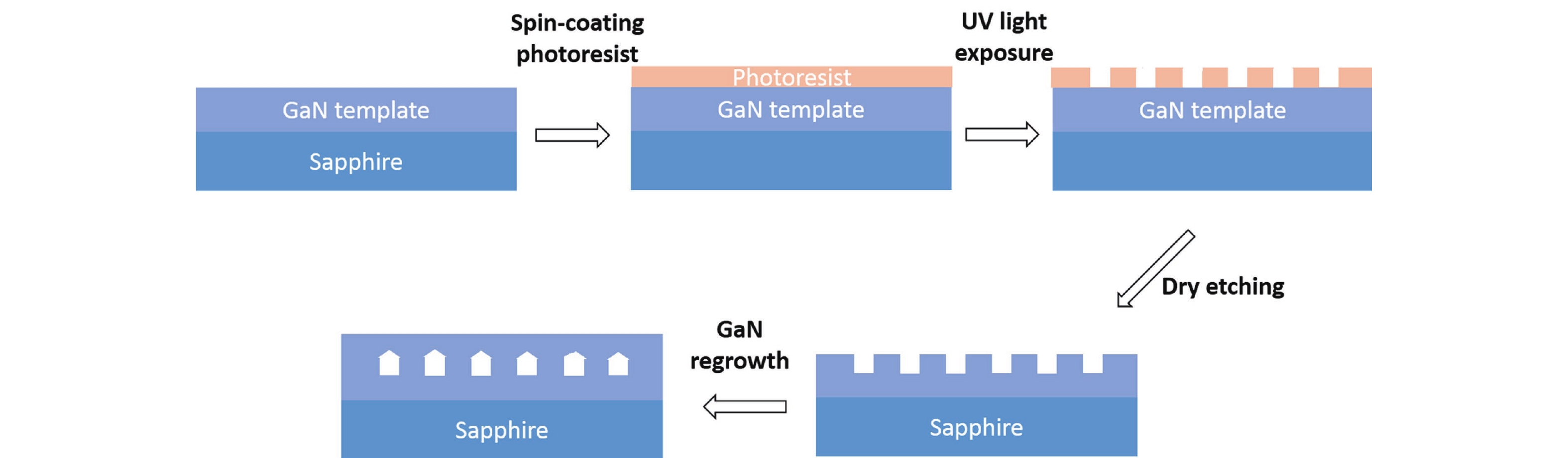
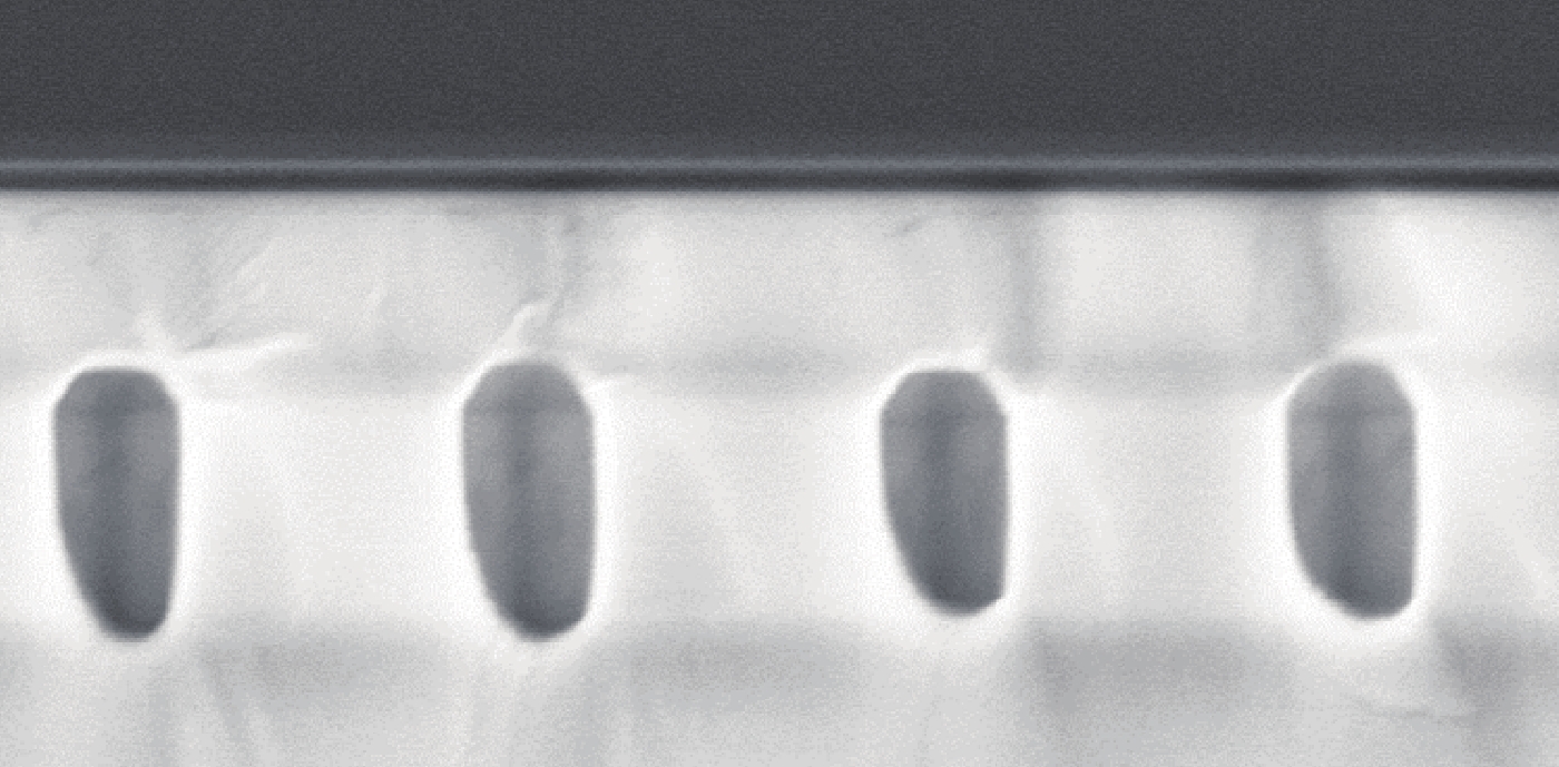
Fig. 1.
(Color online) Schematic of the fabrication process flow to realize Ph-C sample.
ARTICLES
Yunqi Li1, Xinwei Wang2, Ning Zhang2, , Xuecheng Wei2 and Junxi Wang2
Corresponding author: Ning Zhang, zhangn@semi.ac.cn
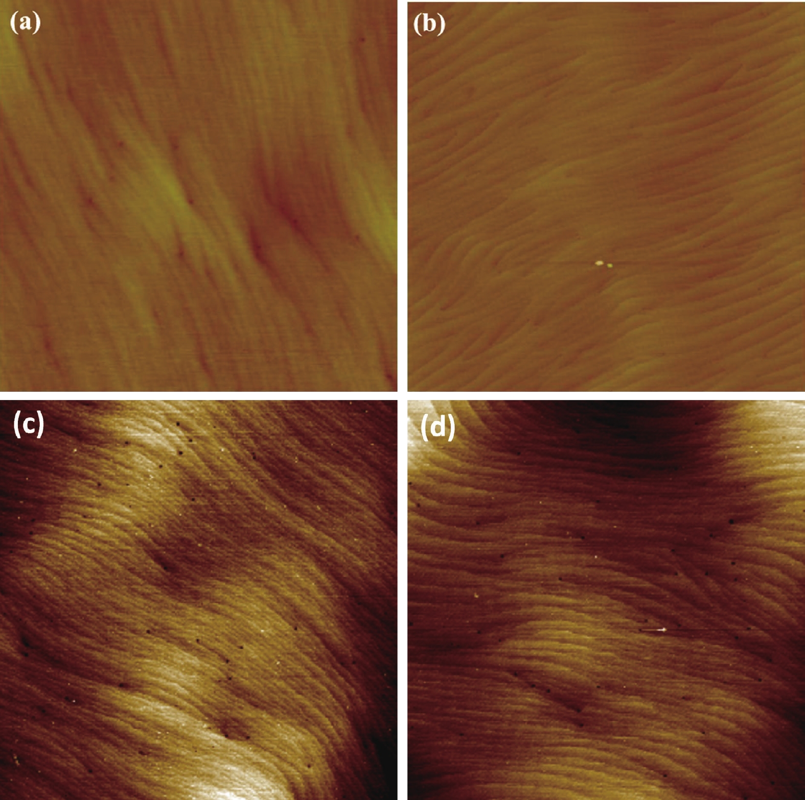
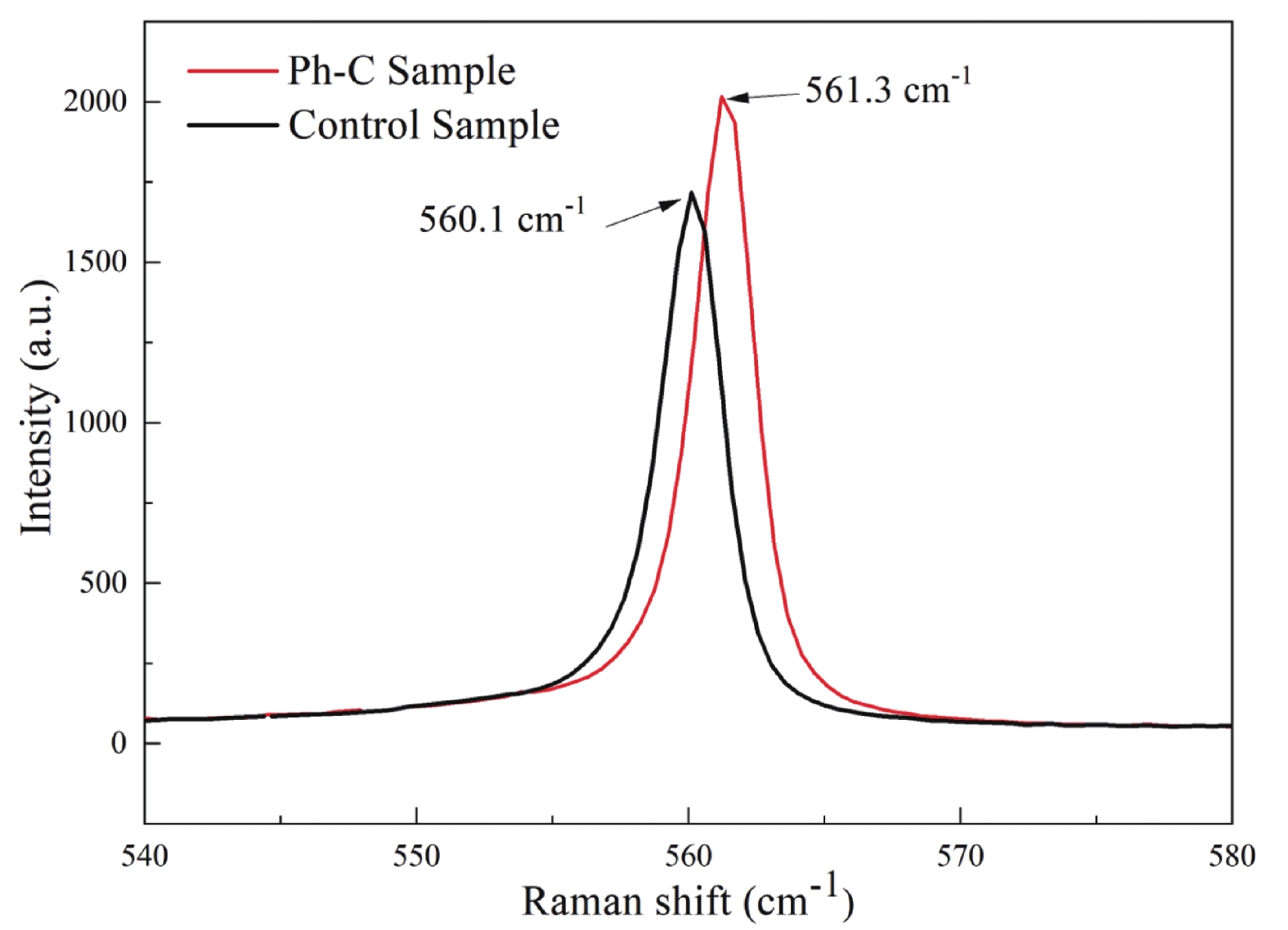
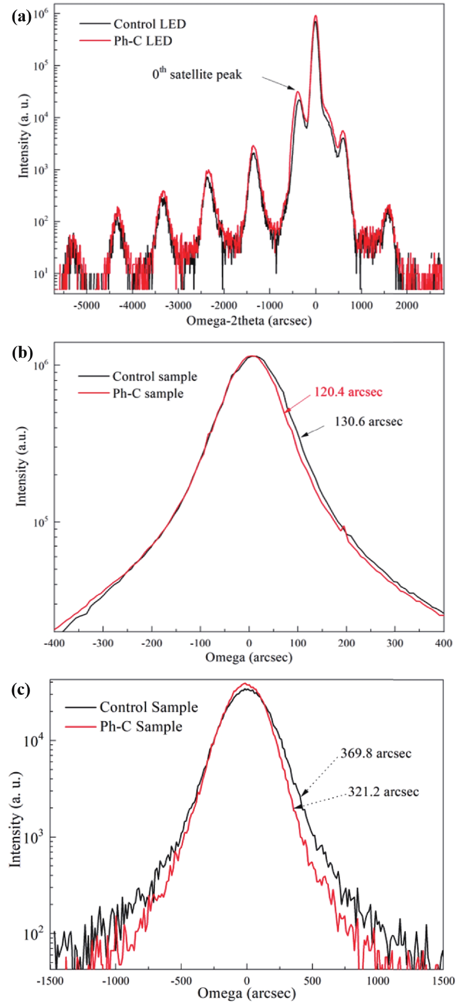
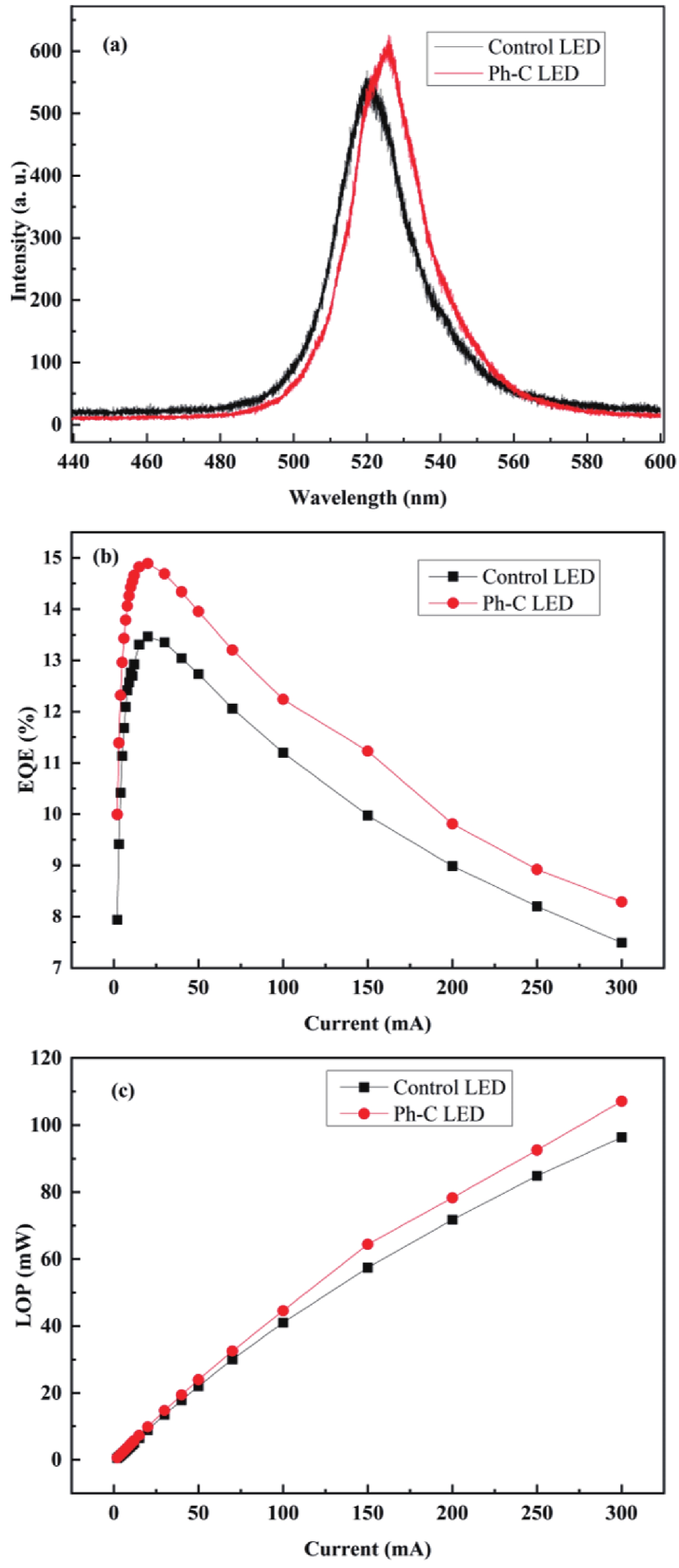
Abstract: We report on the effect of inserted photonic crystalline (Ph-C) in the GaN epitaxial layer on the incorporation of the indium component for the InGaN-based green LED. The adoption of Ph-C in the GaN layer shifted the Raman peak value of E2 mode of GaN to lower frequency and resulted in a tensive stress relief. The stress relief can be attributed to strained lattices restoring in the matrix of Ph-C and the GaN pseudo-epitaxy over the air-void of the Ph-C. Moreover, the HRXRD rocking curves and AFM results show that the insertion of Ph-C also improves the crystal quality. With the inserted Ph-C, the indium component in the multiple quantum wells of the green LED (Ph-C LED) was enhanced. This resulted in a 6-nm red-shift of the peak wavelength. Furthermore, the LOP of the Ph-C LED was enhanced by 10.65% under an injection current of 20 mA.
Key words: epitaxial growth, nanocrystalline materials, semiconductors, Raman, stress relief, X-ray techniques
| [1] |
Strite S. GaN, AlN, and InN: A review. J Vac Sci Technol B, 1992, 10, 1237 doi: 10.1116/1.585897
|
| [2] |
Kisielowski C, Krüger J, Ruvimov S, et al. Strain-related phenomena in GaN thin films. Phys Rev B, 1996, 54, 17745 doi: 10.1103/PhysRevB.54.17745
|
| [3] |
Kozawa T, Kachi T, Kano H, et al. Thermal stress in GaN epitaxial layers grown on sapphire substrates. J Appl Phys, 1995, 77, 4389 doi: 10.1063/1.359465
|
| [4] |
Chen C H, Liao M H, Chang L C, et al. Relaxation of residual stress in bent GaN film on sapphire substrate by laser treatment with an optimized surface structure design. IEEE Trans Electron Devices, 2013, 60, 767 doi: 10.1109/TED.2012.2230330
|
| [5] |
Napierala J, Martin D, Grandjean N, et al. Stress control in GaN/sapphire templates for the fabrication of crack-free thick layers. J Cryst Growth, 2006, 289, 445 doi: 10.1016/j.jcrysgro.2005.11.103
|
| [6] |
Ishikawa H, Zhao G Y, Nakada N, et al. GaN on Si substrate with AlGaN/AlN intermediate layer. Jpn J Appl Phys, 1999, 38, L492 doi: 10.1143/JJAP.38.L492
|
| [7] |
Dadgar A, Bl?sing J, Diez A, et al. Metalorganic chemical vapor phase epitaxy of crack-free GaN on Si (111) exceeding 1 μm in thickness. Jpn J Appl Phys, 2000, 39, L1183 doi: 10.1143/JJAP.39.L1183
|
| [8] |
Feltin E, Beaumont B, Laügt M, et al. Stress control in GaN grown on silicon (111) by metalorganic vapor phase epitaxy. Appl Phys Lett, 2001, 79, 3230 doi: 10.1063/1.1415043
|
| [9] |
Kandaswamy P K, Bougerol C, Jalabert D, et al. Strain relaxation in short-period polar GaN/AlN superlattices. J Appl Phys, 2009, 106, 013526 doi: 10.1063/1.3168431
|
| [10] |
Wang M T, Liao K Y, Li Y L. Growth mechanism and strain variation of GaN material grown on patterned sapphire substrates with various pattern designs. IEEE Photonics Technol Lett, 2011, 23, 962 doi: 10.1109/LPT.2011.2147778
|
| [11] |
Lee J H, Oh J T, Kim Y C, et al. Stress reduction and enhanced extraction efficiency of GaN-based LED grown on cone-shape-patterned sapphire. IEEE Photonics Technol Lett, 2008, 20, 1563 doi: 10.1109/LPT.2008.928844
|
| [12] |
Tseng W J, Gonzalez M, Dillemans L, et al. Strain relaxation in GaN nanopillars. Appl Phys Lett, 2012, 101, 253102 doi: 10.1063/1.4772481
|
| [13] |
Park A H, Seo T H, Chandramohan S, et al. Efficient stress-relaxation in InGaN/GaN light-emitting diodes using carbon nanotubes. Nanoscale, 2015, 7, 15099 doi: 10.1039/C5NR04239A
|
| [14] |
Cheng K, Leys M, Degroote S, et al. Formation of V-grooves on the (Al, Ga)N surface as means of tensile stress relaxation. J Cryst Growth, 2012, 353, 88 doi: 10.1016/j.jcrysgro.2012.05.002
|
| [15] |
Hossain M A, Islam M R. A theoretical calculation of misfit dislocation and strain relaxation in step-graded In xGa1– xN/GaN layers. Adv Mater Res, 2011, 403–408, 456 doi: 10.4028/www.scientific.net/AMR.403-408.456
|
| [16] |
Fu X T, Ma T D, Wang S M, et al. Strain relaxation of GaN heterostructure induced by high-energy electron irradiation. Chin J Rare Met, 2012, 36, 450 doi: 10.3969/j.issn.0258-7076.2012.03.022
|
| [17] |
Young E C, Speck J S. Heteroepitaxial lattice mismatch stress relaxation in nonpolar and semipolar GaN by dislocation glide. ECS Trans, 2013, 50, 797 doi: 10.1149/05009.0797ecst
|
| [18] |
Liu L, Wang L, Li D, et al. Influence of indium composition in the prestrained InGaN interlayer on the strain relaxation of InGaN/ GaN multiple quantum wells in laser diode structures. J Appl Phys, 2011, 109, 073106 doi: 10.1063/1.3569848
|
| [19] |
Won D, Weng X J, Redwing J M. Effect of indium surfactant on stress relaxation by V-defect formation in GaN epilayers grown by metalorganic chemical vapor deposition. J Appl Phys, 2010, 108, 093511 doi: 10.1063/1.3487955
|
| [20] |
Zhang N, Liu Z, Wei T B, et al. Effect of the graded electron blocking layer on the emission properties of GaN-based green light-emitting diodes. Appl Phys Lett, 2012, 100, 053504 doi: 10.1063/1.3681797
|
| [21] |
Du C X, Wei T B, Zheng H Y, et al. Size-controllable nanopyramids photonic crystal selectively grown on p-GaN for enhanced light-extraction of light-emitting diodes. Opt Express, 2013, 21, 25373 doi: 10.1364/OE.21.025373
|
| [22] |
Zhang N, Liu Z, Si Z, et al. Reduction of efficiency droop and modification of polarization fields of InGaN-based green light-emitting diodes via Mg-doping in the barriers. Chin Phys Lett, 2013, 30, 087101 doi: 10.1088/0256-307X/30/8/087101
|
| [23] |
Minj A, Cavalcoli D, Cavallini A, et al. Strain distribution and defect analysis in III-nitrides by dynamical AFM analysis. Nanotechnology, 2013, 24, 145701 doi: 10.1088/0957-4484/24/14/145701
|
| [24] |
Davydov V Y, Kitaev Y E, Goncharuk I N, et al. Phonon dispersion and Raman scattering in hexagonal GaN and AlN. Phys Rev B, 1998, 58, 12899 doi: 10.1103/PhysRevB.58.12899
|
| [25] |
Wagner J M, Bechstedt F. Phonon deformation potentials of α-GaN and-AlN: An ab initio calculation. Appl Phys Lett, 2000, 77, 346 doi: 10.1063/1.127009
|
| [26] |
Jain S C, Willander M, Maes H. Stresses and strains in epilayers, stripes and quantum structures of III-V compound semiconductors. Semicond Sci Technol, 1996, 11, 641 doi: 10.1088/0268-1242/11/5/004
|
| [27] |
Morales F M, González D, Lozano J G, et al. Determination of the composition of In xGa1? xN from strain measurements. Acta Mater, 2009, 57, 5681 doi: 10.1016/j.actamat.2009.07.063
|
| [28] |
Moram M A, Vickers M E. X-ray diffraction of III-nitrides. Rep Prog Phys, 2009, 72, 036502 doi: 10.1088/0034-4885/72/3/036502
|


Article views: 2398 Times PDF downloads: 123 Times Cited by: 0 Times
Received: 24 January 2022 Revised: 04 March 2022 Online: Accepted Manuscript: 17 March 2022Uncorrected proof: 17 March 2022Published: 01 July 2022
| Citation: |
Yunqi Li, Xinwei Wang, Ning Zhang, Xuecheng Wei, Junxi Wang. Improving the incorporation of indium component for InGaN-based green LED through inserting photonic crystalline in the GaN layer[J]. Journal of Semiconductors, 2022, 43(7): 072801. doi: 10.1088/1674-4926/43/7/072801
****
Y Q Li, X W Wang, N Zhang, X C Wei, J X Wang. Improving the incorporation of indium component for InGaN-based green LED through inserting photonic crystalline in the GaN layer[J]. J. Semicond, 2022, 43(7): 072801. doi: 10.1088/1674-4926/43/7/072801

|
| [1] |
Strite S. GaN, AlN, and InN: A review. J Vac Sci Technol B, 1992, 10, 1237 doi: 10.1116/1.585897
|
| [2] |
Kisielowski C, Krüger J, Ruvimov S, et al. Strain-related phenomena in GaN thin films. Phys Rev B, 1996, 54, 17745 doi: 10.1103/PhysRevB.54.17745
|
| [3] |
Kozawa T, Kachi T, Kano H, et al. Thermal stress in GaN epitaxial layers grown on sapphire substrates. J Appl Phys, 1995, 77, 4389 doi: 10.1063/1.359465
|
| [4] |
Chen C H, Liao M H, Chang L C, et al. Relaxation of residual stress in bent GaN film on sapphire substrate by laser treatment with an optimized surface structure design. IEEE Trans Electron Devices, 2013, 60, 767 doi: 10.1109/TED.2012.2230330
|
| [5] |
Napierala J, Martin D, Grandjean N, et al. Stress control in GaN/sapphire templates for the fabrication of crack-free thick layers. J Cryst Growth, 2006, 289, 445 doi: 10.1016/j.jcrysgro.2005.11.103
|
| [6] |
Ishikawa H, Zhao G Y, Nakada N, et al. GaN on Si substrate with AlGaN/AlN intermediate layer. Jpn J Appl Phys, 1999, 38, L492 doi: 10.1143/JJAP.38.L492
|
| [7] |
Dadgar A, Bl?sing J, Diez A, et al. Metalorganic chemical vapor phase epitaxy of crack-free GaN on Si (111) exceeding 1 μm in thickness. Jpn J Appl Phys, 2000, 39, L1183 doi: 10.1143/JJAP.39.L1183
|
| [8] |
Feltin E, Beaumont B, Laügt M, et al. Stress control in GaN grown on silicon (111) by metalorganic vapor phase epitaxy. Appl Phys Lett, 2001, 79, 3230 doi: 10.1063/1.1415043
|
| [9] |
Kandaswamy P K, Bougerol C, Jalabert D, et al. Strain relaxation in short-period polar GaN/AlN superlattices. J Appl Phys, 2009, 106, 013526 doi: 10.1063/1.3168431
|
| [10] |
Wang M T, Liao K Y, Li Y L. Growth mechanism and strain variation of GaN material grown on patterned sapphire substrates with various pattern designs. IEEE Photonics Technol Lett, 2011, 23, 962 doi: 10.1109/LPT.2011.2147778
|
| [11] |
Lee J H, Oh J T, Kim Y C, et al. Stress reduction and enhanced extraction efficiency of GaN-based LED grown on cone-shape-patterned sapphire. IEEE Photonics Technol Lett, 2008, 20, 1563 doi: 10.1109/LPT.2008.928844
|
| [12] |
Tseng W J, Gonzalez M, Dillemans L, et al. Strain relaxation in GaN nanopillars. Appl Phys Lett, 2012, 101, 253102 doi: 10.1063/1.4772481
|
| [13] |
Park A H, Seo T H, Chandramohan S, et al. Efficient stress-relaxation in InGaN/GaN light-emitting diodes using carbon nanotubes. Nanoscale, 2015, 7, 15099 doi: 10.1039/C5NR04239A
|
| [14] |
Cheng K, Leys M, Degroote S, et al. Formation of V-grooves on the (Al, Ga)N surface as means of tensile stress relaxation. J Cryst Growth, 2012, 353, 88 doi: 10.1016/j.jcrysgro.2012.05.002
|
| [15] |
Hossain M A, Islam M R. A theoretical calculation of misfit dislocation and strain relaxation in step-graded In xGa1– xN/GaN layers. Adv Mater Res, 2011, 403–408, 456 doi: 10.4028/www.scientific.net/AMR.403-408.456
|
| [16] |
Fu X T, Ma T D, Wang S M, et al. Strain relaxation of GaN heterostructure induced by high-energy electron irradiation. Chin J Rare Met, 2012, 36, 450 doi: 10.3969/j.issn.0258-7076.2012.03.022
|
| [17] |
Young E C, Speck J S. Heteroepitaxial lattice mismatch stress relaxation in nonpolar and semipolar GaN by dislocation glide. ECS Trans, 2013, 50, 797 doi: 10.1149/05009.0797ecst
|
| [18] |
Liu L, Wang L, Li D, et al. Influence of indium composition in the prestrained InGaN interlayer on the strain relaxation of InGaN/ GaN multiple quantum wells in laser diode structures. J Appl Phys, 2011, 109, 073106 doi: 10.1063/1.3569848
|
| [19] |
Won D, Weng X J, Redwing J M. Effect of indium surfactant on stress relaxation by V-defect formation in GaN epilayers grown by metalorganic chemical vapor deposition. J Appl Phys, 2010, 108, 093511 doi: 10.1063/1.3487955
|
| [20] |
Zhang N, Liu Z, Wei T B, et al. Effect of the graded electron blocking layer on the emission properties of GaN-based green light-emitting diodes. Appl Phys Lett, 2012, 100, 053504 doi: 10.1063/1.3681797
|
| [21] |
Du C X, Wei T B, Zheng H Y, et al. Size-controllable nanopyramids photonic crystal selectively grown on p-GaN for enhanced light-extraction of light-emitting diodes. Opt Express, 2013, 21, 25373 doi: 10.1364/OE.21.025373
|
| [22] |
Zhang N, Liu Z, Si Z, et al. Reduction of efficiency droop and modification of polarization fields of InGaN-based green light-emitting diodes via Mg-doping in the barriers. Chin Phys Lett, 2013, 30, 087101 doi: 10.1088/0256-307X/30/8/087101
|
| [23] |
Minj A, Cavalcoli D, Cavallini A, et al. Strain distribution and defect analysis in III-nitrides by dynamical AFM analysis. Nanotechnology, 2013, 24, 145701 doi: 10.1088/0957-4484/24/14/145701
|
| [24] |
Davydov V Y, Kitaev Y E, Goncharuk I N, et al. Phonon dispersion and Raman scattering in hexagonal GaN and AlN. Phys Rev B, 1998, 58, 12899 doi: 10.1103/PhysRevB.58.12899
|
| [25] |
Wagner J M, Bechstedt F. Phonon deformation potentials of α-GaN and-AlN: An ab initio calculation. Appl Phys Lett, 2000, 77, 346 doi: 10.1063/1.127009
|
| [26] |
Jain S C, Willander M, Maes H. Stresses and strains in epilayers, stripes and quantum structures of III-V compound semiconductors. Semicond Sci Technol, 1996, 11, 641 doi: 10.1088/0268-1242/11/5/004
|
| [27] |
Morales F M, González D, Lozano J G, et al. Determination of the composition of In xGa1? xN from strain measurements. Acta Mater, 2009, 57, 5681 doi: 10.1016/j.actamat.2009.07.063
|
| [28] |
Moram M A, Vickers M E. X-ray diffraction of III-nitrides. Rep Prog Phys, 2009, 72, 036502 doi: 10.1088/0034-4885/72/3/036502
|

 WeChat ID
Journal of Semiconductors © 2017 All Rights Reserved 京ICP備05085259號-2
 DownLoad:

