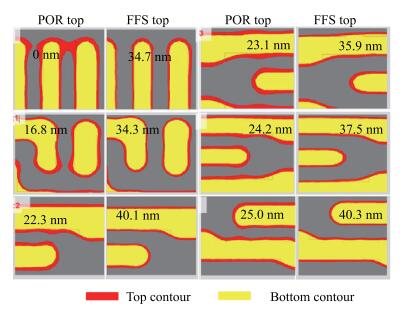
Fig. 1.
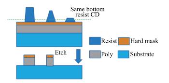
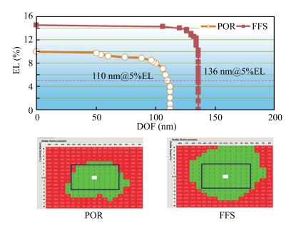
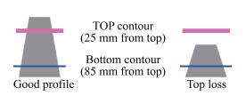
At 2x node, resist top loss and sidewall angle variation.
SEMICONDUCTOR DEVICES
Jun Zhu1, Wei Zhang1, Chinte Kuo1, Qing Wang2, , Fang Wei2, Chenming Zhang2, Han Chen2, Daquan He2 and D. Hsu Stephen3
Corresponding author: Qing Wang, Email: qangever@126.com
Abstract: As technology node shrinks, aggressive design rules for contact and other back end of line (BEOL) layers continue to drive the need for more effective full chip patterning optimization. Resist top loss is one of the major challenges for 28 nm and below technology nodes, which can lead to post-etch hotspots that are difficult to predict and eventually degrade the process window significantly. To tackle this problem, we used an advanced programmable illuminator (FlexRay) and Tachyon SMO (Source Mask Optimization) platform to make resist-aware source optimization possible, and it is proved to greatly improve the imaging contrast, enhance focus and exposure latitude, and minimize resist top loss thus improving the yield.
Key words: integrated circuits, OPC, source optimization, lithography, resist top loss
| [1] |
Hsu S, Chen L, Liu H Y, et al. An innovative source-mask co-optimization (SMO) method for extending low k1 imaging. Proc SPIE, 2008, 7140(12): 714010 https://www.researchgate.net/publication/229001493_An_Innovative_Source-Mask_co-Optimization_SMO_Method_for_Extending_Low_k1_Imaging
|
| [2] |
Hsu S, Chen L, Liu H, et al. Source-mask cooptimization: optimize design for imaging and impact of source complexity on lithography performance. Proc SPIE, 2009, 7520(7): 712008 https://www.researchgate.net/publication/252623150_Source-mask_co-optimization_Optimize_design_for_imaging_and_impact_of_source_complexity_on_lithography_performance?ev=auth_pub
|
| [3] |
Zhang D Q, Chua G S, Foong Y M, et al. Source mask optimization methodology (SMO) & application to real full chip optical proximity correction. Proc SPIE, 2012, 8326: 83261V-11 doi: 10.1117/12.916614
|
| [4] |
Chen A, Foong Y M, Khoh A, et al. Resist profile aware source mask optimization. Proc SPIE, 2014, 9053(1): 43
|
| [5] |
Wang Z H, Liu W, Wang L, et al. Key process study in nanoimprint lithography. J Semicond, 2012, 33(10): 106002 doi: 10.1088/1674-4926/33/10/106002
|
| [6] |
Setten E V, Oorschot D, Manet C W, et al. EUV mask stack optimization for enhanced imaging performance. Proc SPIE, 2010, 7823(10): 782312
|
| [7] |
Zhou K J, Wang P J, Wen L. Design of power balance SRAM for DPA-resistance. J Semicond, 2016, 37(4): 045002 doi: 10.1088/1674-4926/37/4/045002
|
| [8] |
Yu J C, Yu P, Chao H Y. Fast source optimization involving quadratic line-contour objectives for the resist image. Opt Express, 2012, 20(7): 8161 doi: 10.1364/OE.20.008161
|
| [9] |
Xie C L, Chen Y, Shi Z. A novel OPC method to reduce mask volume with yield-aware dissection. J Semicond, 2013, 34(10): 106002 doi: 10.1088/1674-4926/34/10/106002
|
| [10] |
Yu M Y, Li T, Yang J Q, et al. A 1 V 186-μW 50-MS/s 10-bit subrange SAR ADC in 130-nm CMOS process. J Semicond, 2016, 37(7): 075005 doi: 10.1088/1674-4926/37/7/075005
|
| [11] |
Song Z, Ma X, Gao J, et al. Inverse lithography source optimization via compressive sensing. Opt Express, 2014, 22(12): 14180 doi: 10.1364/OE.22.014180
|
| [12] |
Zhong S, Zhu Z M. A 0.1-1.5 GHz, low jitter, area efficient PLL in 55-nm CMOS process. J Semicond, 2016, 37(5): 055004 doi: 10.1088/1674-4926/37/5/055004
|
| [13] |
Pang L, Xiao G, Tolani V, et al. Inverse lithography technology (ILT) enabled source mask optimization (SMO). ECS Trans, 2009, 18(1): 299 http://d.wanfangdata.com.cn/Conference/WFHYXW355775
|
| [14] |
Koops H W P, Kretz J, Weber M. Combined lithographies for the reduction of stitching errors in lithography. J Vac Sci Technol B, 1994, 12(6): 3265 doi: 10.1116/1.587609
|
| [15] |
Li J, Shen Y, Lam E Y. Hotspot-aware fast source and mask optimization. Opt Express, 2012, 20(19): 21792 doi: 10.1364/OE.20.021792
|
| [16] |
Granik Y. Source optimization for image fidelity and throughput. J Microlithography Microfabric Microsyst, 2007, 3(4): 509
|
| [17] |
Clerc F, Farrusseng D, Mirodatos C. A versatile open-source optimization platform for experimental design. Chemometrics & Intelligent Laboratory Systems, 2008, 93(2): 167 https://www.researchgate.net/publication/223350594_OptiCat_A_versatile_open-source_optimization_platform_for_experimental_design
|
| [18] |
Erdmann A, Farkas R, Fuehner T, et al. Mask and source optimization for lithographic imaging systems. Proc SPIE, 2003: 5182
|


Article views: 6039 Times PDF downloads: 87 Times Cited by: 0 Times
Received: 18 December 2016 Revised: 10 January 2017 Online: Published: 01 July 2017
| Citation: |
Jun Zhu, Wei Zhang, Chinte Kuo, Qing Wang, Fang Wei, Chenming Zhang, Han Chen, Daquan He, D. Hsu Stephen. Application of resist-profile-aware source optimization in 28 nm full chip optical proximity correction[J]. Journal of Semiconductors, 2017, 38(7): 074007. doi: 10.1088/1674-4926/38/7/074007
****
J Zhu, W Zhang, C N T Kuo, Q Wang, F Wei, C M Zhang, H Chen, D Q He, D H Stephen. Application of resist-profile-aware source optimization in 28 nm full chip optical proximity correction[J]. J. Semicond., 2017, 38(7): 074007. doi:? 10.1088/1674-4926/38/7/074007.

|
| [1] |
Hsu S, Chen L, Liu H Y, et al. An innovative source-mask co-optimization (SMO) method for extending low k1 imaging. Proc SPIE, 2008, 7140(12): 714010 https://www.researchgate.net/publication/229001493_An_Innovative_Source-Mask_co-Optimization_SMO_Method_for_Extending_Low_k1_Imaging
|
| [2] |
Hsu S, Chen L, Liu H, et al. Source-mask cooptimization: optimize design for imaging and impact of source complexity on lithography performance. Proc SPIE, 2009, 7520(7): 712008 https://www.researchgate.net/publication/252623150_Source-mask_co-optimization_Optimize_design_for_imaging_and_impact_of_source_complexity_on_lithography_performance?ev=auth_pub
|
| [3] |
Zhang D Q, Chua G S, Foong Y M, et al. Source mask optimization methodology (SMO) & application to real full chip optical proximity correction. Proc SPIE, 2012, 8326: 83261V-11 doi: 10.1117/12.916614
|
| [4] |
Chen A, Foong Y M, Khoh A, et al. Resist profile aware source mask optimization. Proc SPIE, 2014, 9053(1): 43
|
| [5] |
Wang Z H, Liu W, Wang L, et al. Key process study in nanoimprint lithography. J Semicond, 2012, 33(10): 106002 doi: 10.1088/1674-4926/33/10/106002
|
| [6] |
Setten E V, Oorschot D, Manet C W, et al. EUV mask stack optimization for enhanced imaging performance. Proc SPIE, 2010, 7823(10): 782312
|
| [7] |
Zhou K J, Wang P J, Wen L. Design of power balance SRAM for DPA-resistance. J Semicond, 2016, 37(4): 045002 doi: 10.1088/1674-4926/37/4/045002
|
| [8] |
Yu J C, Yu P, Chao H Y. Fast source optimization involving quadratic line-contour objectives for the resist image. Opt Express, 2012, 20(7): 8161 doi: 10.1364/OE.20.008161
|
| [9] |
Xie C L, Chen Y, Shi Z. A novel OPC method to reduce mask volume with yield-aware dissection. J Semicond, 2013, 34(10): 106002 doi: 10.1088/1674-4926/34/10/106002
|
| [10] |
Yu M Y, Li T, Yang J Q, et al. A 1 V 186-μW 50-MS/s 10-bit subrange SAR ADC in 130-nm CMOS process. J Semicond, 2016, 37(7): 075005 doi: 10.1088/1674-4926/37/7/075005
|
| [11] |
Song Z, Ma X, Gao J, et al. Inverse lithography source optimization via compressive sensing. Opt Express, 2014, 22(12): 14180 doi: 10.1364/OE.22.014180
|
| [12] |
Zhong S, Zhu Z M. A 0.1-1.5 GHz, low jitter, area efficient PLL in 55-nm CMOS process. J Semicond, 2016, 37(5): 055004 doi: 10.1088/1674-4926/37/5/055004
|
| [13] |
Pang L, Xiao G, Tolani V, et al. Inverse lithography technology (ILT) enabled source mask optimization (SMO). ECS Trans, 2009, 18(1): 299 http://d.wanfangdata.com.cn/Conference/WFHYXW355775
|
| [14] |
Koops H W P, Kretz J, Weber M. Combined lithographies for the reduction of stitching errors in lithography. J Vac Sci Technol B, 1994, 12(6): 3265 doi: 10.1116/1.587609
|
| [15] |
Li J, Shen Y, Lam E Y. Hotspot-aware fast source and mask optimization. Opt Express, 2012, 20(19): 21792 doi: 10.1364/OE.20.021792
|
| [16] |
Granik Y. Source optimization for image fidelity and throughput. J Microlithography Microfabric Microsyst, 2007, 3(4): 509
|
| [17] |
Clerc F, Farrusseng D, Mirodatos C. A versatile open-source optimization platform for experimental design. Chemometrics & Intelligent Laboratory Systems, 2008, 93(2): 167 https://www.researchgate.net/publication/223350594_OptiCat_A_versatile_open-source_optimization_platform_for_experimental_design
|
| [18] |
Erdmann A, Farkas R, Fuehner T, et al. Mask and source optimization for lithographic imaging systems. Proc SPIE, 2003: 5182
|

 WeChat ID
Journal of Semiconductors © 2017 All Rights Reserved 京ICP備05085259號-2
 DownLoad: