


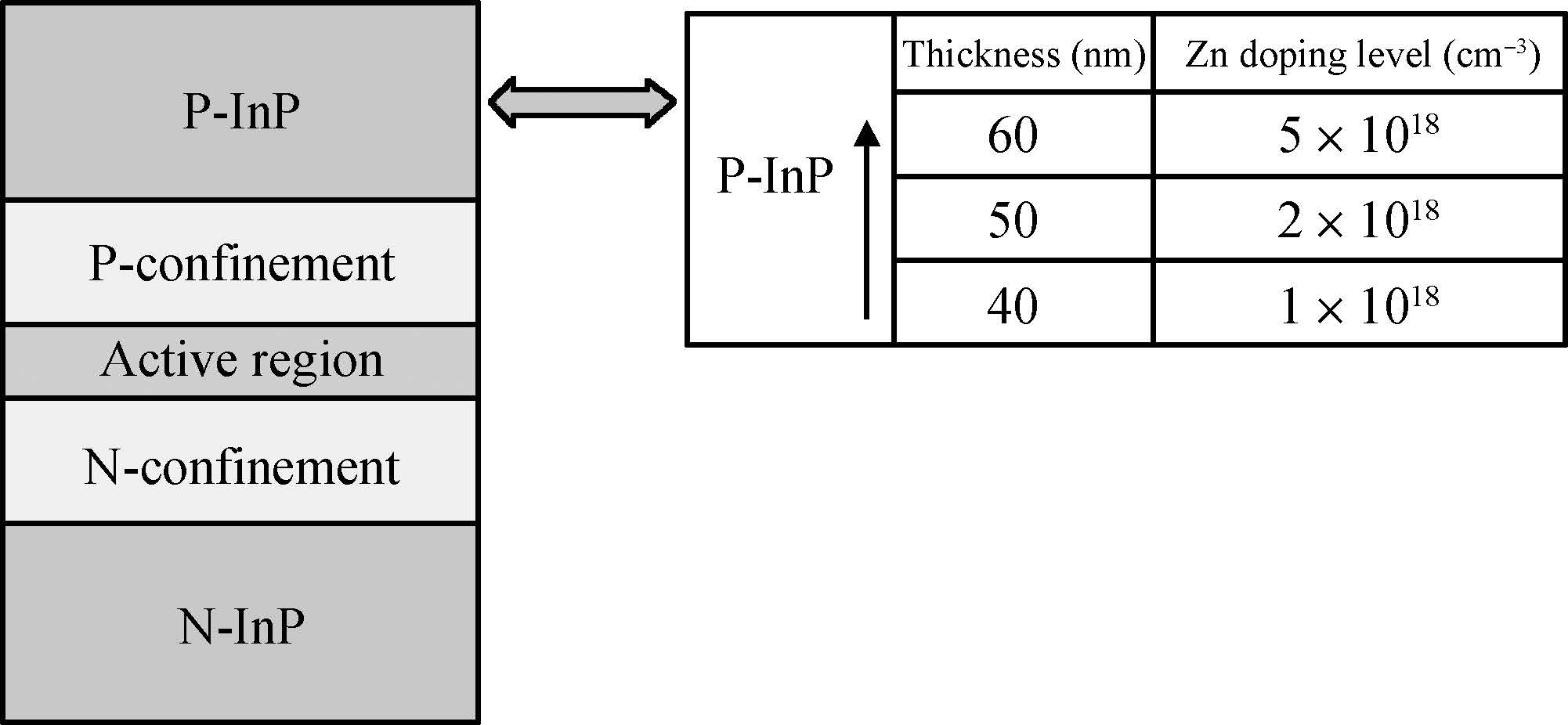
Fig. 1.
Schematic diagram of the 1.55 $\mu $m MQW laser epitaxial structure.
SEMICONDUCTOR DEVICES
Qing Ke, Shaoyang Tan, Songtao Liu, Dan Lu, Ruikang Zhang, Wei Wang and Chen Ji
Corresponding author: Ke Qing, keqing12@semi.ac.cn
Abstract: A comprehensive design optimization of 1.55-μm high power InGaAsP/InP board area lasers is performed aiming at increasing the internal quantum efficiency (ηi) while maintaining the low internal loss (αi) of the device, thereby achieving high power operation. Four different waveguide structures of broad area lasers were fabricated and characterized in depth. Through theoretical analysis and experiment verifications, we show that laser structures with stepped waveguide and thin upper separate confinement layer will result in high ηi and overall slope efficiency. A continuous wave (CW) single side output power of 160 mW was obtained for an uncoated laser with a 50-μm active area width and 1 mm cavity length.
Key words: high power, laser, InP, internal loss, internal quantum efficiency
| [1] | |
| [2] | |
| [3] | |
| [4] | |
| [5] | |
| [6] | |
| [7] | |
| [8] | |
| [9] | |
| [10] | |
| [11] | |
| [12] |
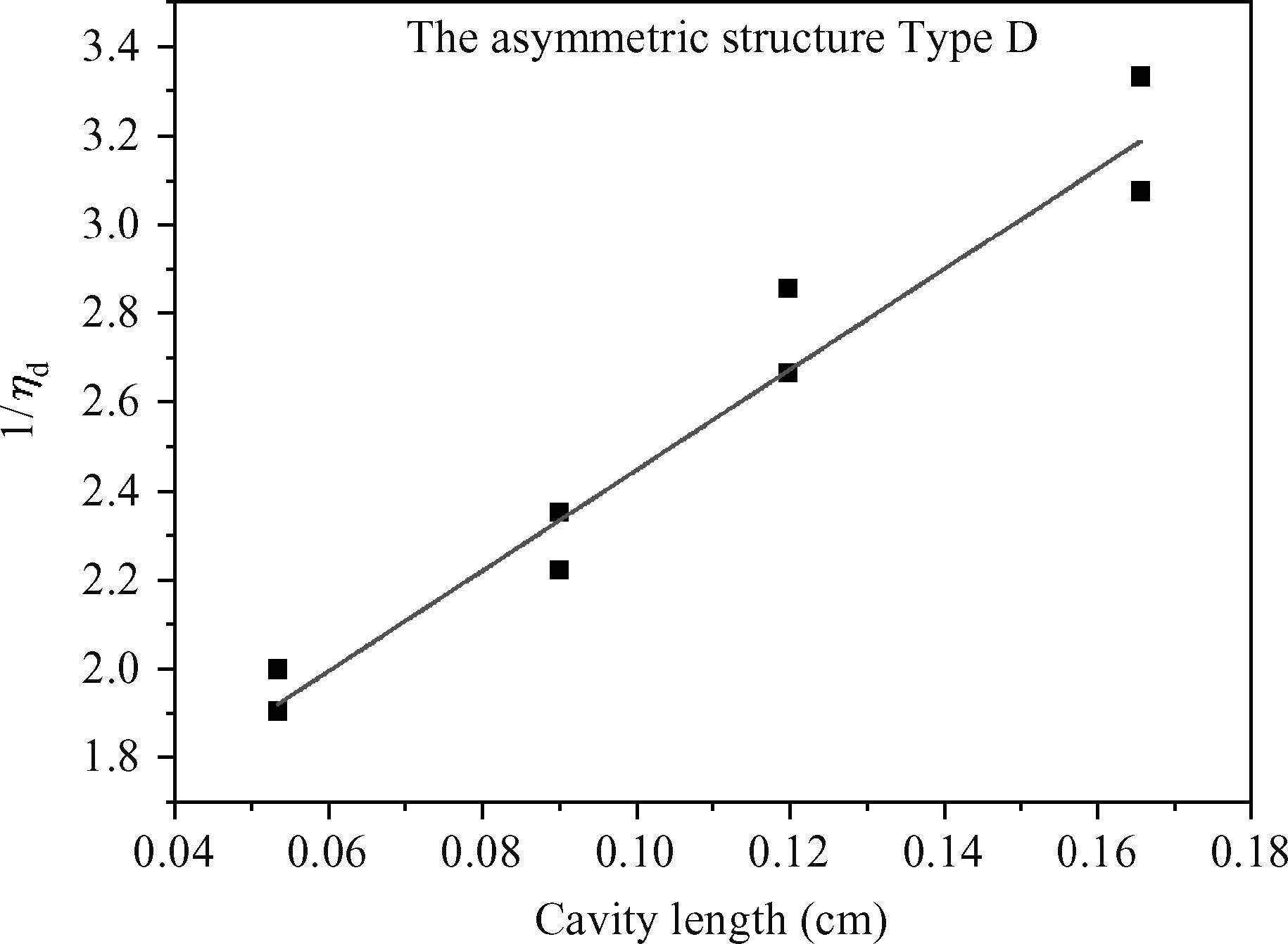
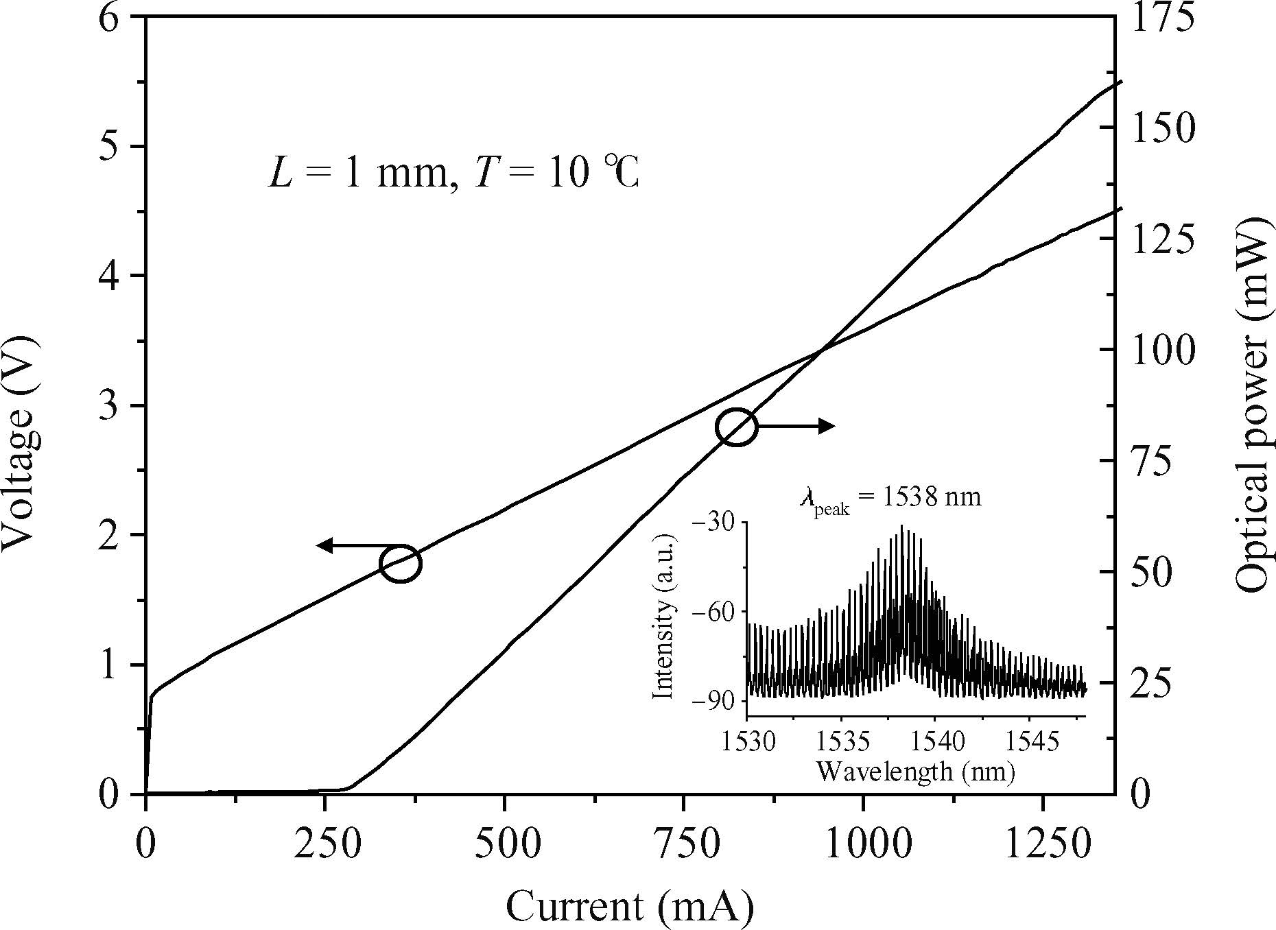
Table 1. Active region design parameters,experimental $\alpha_{\rm i}$ and $\eta_{\rm i}$ values,calculated $\alpha_{\rm i}$,and two side slope efficiency at $L=$ 1 mm (Types A-D).
 DownLoad: CSV
| [1] | |
| [2] | |
| [3] | |
| [4] | |
| [5] | |
| [6] | |
| [7] | |
| [8] | |
| [9] | |
| [10] | |
| [11] | |
| [12] |


Article views: 5477 Times PDF downloads: 234 Times Cited by: 0 Times
Received: 09 February 2015 Revised: Online: Published: 01 September 2015
| Citation: |
Qing Ke, Shaoyang Tan, Songtao Liu, Dan Lu, Ruikang Zhang, Wei Wang, Chen Ji. Fabrication and optimization of 1.55-μm InGaAsP/InP high-power semiconductor diode laser[J]. Journal of Semiconductors, 2015, 36(9): 094010. doi: 10.1088/1674-4926/36/9/094010
****
Q Ke, S Y Tan, S T Liu, D Lu, R K Zhang, W Wang, C Ji. Fabrication and optimization of 1.55-μm InGaAsP/InP high-power semiconductor diode laser[J]. J. Semicond., 2015, 36(9): 094010. doi: 10.1088/1674-4926/36/9/094010.

|
Project supported by the National Natural Science Foundation of China (Nos. 61274046, 61201103) and the National High Technology Research and Development Program of China (No. 2013AA014202).
| [1] | |
| [2] | |
| [3] | |
| [4] | |
| [5] | |
| [6] | |
| [7] | |
| [8] | |
| [9] | |
| [10] | |
| [11] | |
| [12] |

 WeChat ID
Journal of Semiconductors © 2017 All Rights Reserved 京ICP備05085259號-2

