


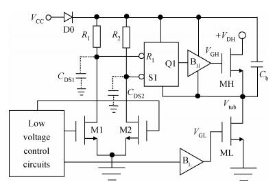
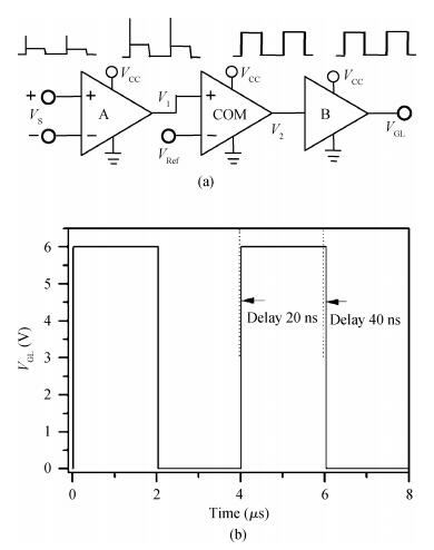
Fig. 1.
The schematic circuit diagram of a half-bridge HVIC
SEMICONDUCTOR DEVICES
Corresponding author: Kong Moufu, Email:kongmoufu@163.com
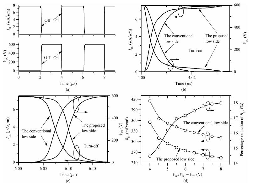
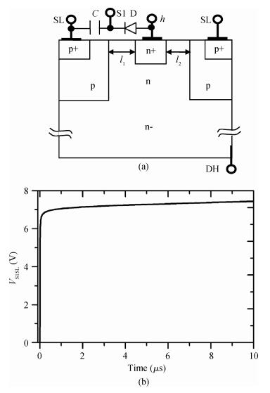
Abstract: Novel high-voltage, high-side and low-side power devices, whose control circuits are referred to as the tub, are proposed and investigated to reduce chip area and improve the reliability of high-voltage integrated circuits. By using the tub circuit to control a branch circuit consisting of a PMOS and a resistor, a pulse signal is generated to control the low-side n-LDMOS after being processed by a low-voltage circuit. Thus, the high-voltage level-shifting circuit is not needed any more, and the parasitic effect of the conventional level-shifting circuit is eliminated. Moreover, the specific on-resistance of the proposed low-side device is reduced by more than 14.3% compared with the conventional one. In the meantime, integrated low-voltage power supplies for the low-voltage circuit and the tub circuit are also proposed. Simulations are performed with MEDICI and SPICE, and the results show that the expectant functions are achieved well.
Key words: power devices, LDMOS, pulse signal, low-voltage power supply
| [1] |
He J, Zhang Xing. Analytical model of surface field distribution and breakdown voltage for RESURF LDMOS transistor. Chinese Journal of Semiconductors, 2001, 22(9):1102 http://en.cnki.com.cn/Article_en/CJFDTOTAL-BDTX200109001.htm
|
| [2] |
Chen Xingbi. Lateral low-side and high-side high-voltage devices. US Patent, No. 6998681, 2006
|
| [3] |
Kim J J, Kim M H, Kim S L, et al. The new high voltage level up shifter for HVIC. IEEE 33rd Annual Power Electronics Specialists Conference, 2002, 2:626 http://ieeexplore.ieee.org/document/1022523/
|
| [4] |
Terashima T, Shimizu K, Hine S. A new level-shifting technique by divided RESURF structure. International Symposium on Power Semiconductor Devices and IC's, ISPSD, 1997:57 http://ieeexplore.ieee.org/document/601431/authors
|
| [5] |
Hossain Z. Determination of manufacturing RESURF process window for a robust 700 V double RESURF LDMOS transistor. Proceedings of the 20th International Symposium on Power Semiconductor Devices & IC's, 2008:133 http://ieeexplore.ieee.org/document/4538916/authors
|
| [6] |
Jeon C K, Kim J J, Choi Y S, et al. Analysis of LDMOS structure with inclined p-bottom region. Power Semiconductor Devices and ICs, Proceedings of the 14th International Symposium, 2002:293 http://ieeexplore.ieee.org/document/1016229/keywords
|
| [7] |
Shimizu K, Terashima T. The 2nd generation divided RESURF structure for high voltage ICs. 20th International Symposium on Power Semiconductor Devices and IC's (ISPSD), 2008:311 http://ieeexplore.ieee.org/document/4538961/
|
| [8] |
Chen Xingbi. Surface voltage sustaining structure for semiconductor devices. US Patent, No. 5726469, 1998
|
| [9] |
Chen X B, Zhang B, Li Z J. Theory of optimum design of reverse-biased p-n junctions using resistive field plates and variation lateral doping. Solid-State Electron, 1992, 35(9):1365 doi: 10.1016/0038-1101(92)90173-A
|
| [10] |
Chen X, Fan X. Optimum VLD makes SPIC better and cheaper. 6th International Conference on Solid-State and Integrated-Circuit Technology, 2001, 1:104 http://ieeexplore.ieee.org/document/981433/
|
| [11] |
Du Wenfang, Chen Xingbi. A study of second saturation effect of OPTVLD NMOS. 9th IEEE International Conference on ASIC, 2011:551 http://ieeexplore.ieee.org/abstract/document/6157264/
|
| [12] |
Kong M F, Chen X B. High voltage low side and high side power devices based on VLD technique. IEEE 11th International Conference on Solid-State and Integrated Circuit Technology (ICSICT), 2012:1 http://ieeexplore.ieee.org/document/6466709/
|
| [13] |
Rossberg M, Vogler B, Herzer R. 600 V SOI gate driver IC with advanced level shifter concepts for medium and high power applications. European Conference on Power Electronics and Applications, 2007:1
|
| [14] |
Liu Jizhi, Chen Xingbi. A new level-shifting structure with multiply metal rings by divided RESURF technique. Journal of Semiconductors, 2009, 30(4):044005 doi: 10.1088/1674-4926/30/4/044005
|
| [15] |
Marari B, Bertotti F, Vignola G A, et al. Smart power ICs:technologies and applications. Springer Verlag, Berlin, Heidelberg, New York, 1995:361
|
| [16] |
Chen X B. Method of producing a low-voltage power supply in a power integrated circuit. US Patent, No. 7701006, 2010
|


Article views: 3470 Times PDF downloads: 28 Times Cited by: 0 Times
Received: 21 March 2013 Revised: 03 May 2013 Online: Published: 01 September 2013
| Citation: |
Moufu Kong, Xingbi Chen. Novel high-voltage, high-side and low-side power devices with a single control signal[J]. Journal of Semiconductors, 2013, 34(9): 094009. doi: 10.1088/1674-4926/34/9/094009
****
M F Kong, X B Chen. Novel high-voltage, high-side and low-side power devices with a single control signal[J]. J. Semicond., 2013, 34(9): 094009. doi: 10.1088/1674-4926/34/9/094009.

|
Project supported by the 2011 Ph.D. Programs Foundation of the Ministry of Education of China (No. 20110185110003)
the 2011 Ph.D. Programs Foundation of the Ministry of Education of China 20110185110003
| [1] |
He J, Zhang Xing. Analytical model of surface field distribution and breakdown voltage for RESURF LDMOS transistor. Chinese Journal of Semiconductors, 2001, 22(9):1102 http://en.cnki.com.cn/Article_en/CJFDTOTAL-BDTX200109001.htm
|
| [2] |
Chen Xingbi. Lateral low-side and high-side high-voltage devices. US Patent, No. 6998681, 2006
|
| [3] |
Kim J J, Kim M H, Kim S L, et al. The new high voltage level up shifter for HVIC. IEEE 33rd Annual Power Electronics Specialists Conference, 2002, 2:626 http://ieeexplore.ieee.org/document/1022523/
|
| [4] |
Terashima T, Shimizu K, Hine S. A new level-shifting technique by divided RESURF structure. International Symposium on Power Semiconductor Devices and IC's, ISPSD, 1997:57 http://ieeexplore.ieee.org/document/601431/authors
|
| [5] |
Hossain Z. Determination of manufacturing RESURF process window for a robust 700 V double RESURF LDMOS transistor. Proceedings of the 20th International Symposium on Power Semiconductor Devices & IC's, 2008:133 http://ieeexplore.ieee.org/document/4538916/authors
|
| [6] |
Jeon C K, Kim J J, Choi Y S, et al. Analysis of LDMOS structure with inclined p-bottom region. Power Semiconductor Devices and ICs, Proceedings of the 14th International Symposium, 2002:293 http://ieeexplore.ieee.org/document/1016229/keywords
|
| [7] |
Shimizu K, Terashima T. The 2nd generation divided RESURF structure for high voltage ICs. 20th International Symposium on Power Semiconductor Devices and IC's (ISPSD), 2008:311 http://ieeexplore.ieee.org/document/4538961/
|
| [8] |
Chen Xingbi. Surface voltage sustaining structure for semiconductor devices. US Patent, No. 5726469, 1998
|
| [9] |
Chen X B, Zhang B, Li Z J. Theory of optimum design of reverse-biased p-n junctions using resistive field plates and variation lateral doping. Solid-State Electron, 1992, 35(9):1365 doi: 10.1016/0038-1101(92)90173-A
|
| [10] |
Chen X, Fan X. Optimum VLD makes SPIC better and cheaper. 6th International Conference on Solid-State and Integrated-Circuit Technology, 2001, 1:104 http://ieeexplore.ieee.org/document/981433/
|
| [11] |
Du Wenfang, Chen Xingbi. A study of second saturation effect of OPTVLD NMOS. 9th IEEE International Conference on ASIC, 2011:551 http://ieeexplore.ieee.org/abstract/document/6157264/
|
| [12] |
Kong M F, Chen X B. High voltage low side and high side power devices based on VLD technique. IEEE 11th International Conference on Solid-State and Integrated Circuit Technology (ICSICT), 2012:1 http://ieeexplore.ieee.org/document/6466709/
|
| [13] |
Rossberg M, Vogler B, Herzer R. 600 V SOI gate driver IC with advanced level shifter concepts for medium and high power applications. European Conference on Power Electronics and Applications, 2007:1
|
| [14] |
Liu Jizhi, Chen Xingbi. A new level-shifting structure with multiply metal rings by divided RESURF technique. Journal of Semiconductors, 2009, 30(4):044005 doi: 10.1088/1674-4926/30/4/044005
|
| [15] |
Marari B, Bertotti F, Vignola G A, et al. Smart power ICs:technologies and applications. Springer Verlag, Berlin, Heidelberg, New York, 1995:361
|
| [16] |
Chen X B. Method of producing a low-voltage power supply in a power integrated circuit. US Patent, No. 7701006, 2010
|

 WeChat ID
Journal of Semiconductors © 2017 All Rights Reserved 京ICP備05085259號-2
 DownLoad:

