


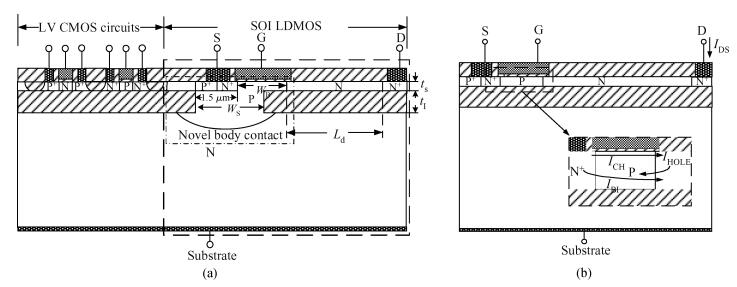
Fig. 1.
Schematic cross sections of (a) the proposed SOI LDMOS in a PIC and (b) the FB SOI LDMOS, with various current components marked
SEMICONDUCTOR DEVICES
Yongheng Jiang, Xiaorong Luo, Yanfei Li, Pei Wang, Ye Fan, Kun Zhou, Qi Wang, Xiarong Hu and Bo Zhang
Corresponding author: Luo Xiaorong, Email:xrluo@uestc.edu.cn
Abstract: A novel CMOS-compatible thin film SOI LDMOS with a novel body contact structure is proposed. It has a Si window and a P-body extended to the substrate through the Si window, thus, the P-body touches the P+ region to form the body contact. Compared with the conventional floating body SOI LDMOS (FB SOI LDMOS) structure, the new structure increases the off-state BV by 54%, decreases the specific on resistance by 20%, improves the output characteristics significantly, and suppresses the self-heating effect. Furthermore, the advantages of the low leakage current and low output capacitance of SOI devices do not degrade.
Key words: thin film SOI LDMOS, body contact, floating body effect, parasitic BJT effect
| [1] |
Colinge J P. Silicon-on-insulator technology:materials to VLSI, 2nd ed. Netherlands:Kluwer Academic Publisher, 1997:123
|
| [2] |
Xue S B, Huang R, Huang D T, et al. Impact of the displacement damage in channel and source/drain regions on the DC characteristics degradation in deep-submicron MOSFETs after heavy ion irradiation. Chin Phys B, 2010, 19(11):117307 doi: 10.1088/1674-1056/19/11/117307
|
| [3] |
Choi J Y, Fossum J G. Analysis and control of floating-body bipolar effects in fully depleted submicrometer SOI MOSFET's. IEEE Trans Electron Devices, 1991, 38(6):1384 doi: 10.1109/16.81630
|
| [4] |
Eric P Ver P, Cuong T N, Simon W S, et al. Parasitic bipolar gain in fully depleted n-channel SOI MOSFET's. IEEE Trans Electron Devices, 1994, 41(6):970 doi: 10.1109/16.293310
|
| [5] |
Chen C E D, Mishel M, Sundaresan R, et al. Single-transistor latch in SOI MOSFET's. IEEE Electron Device Lett, 1988, 9(12):636 doi: 10.1109/55.20420
|
| [6] |
Liu Y L, Liu X Y, Han Z S, et al. Simulation of a novel Schottky body-contacted structure suppressing floating body effect in partially-depleted SOI nMOSFET's. Chinese Journal of Semiconductors, 2002, 23(10):1019
|
| [7] |
Cheng X H, Yang W W, Song Z R, et al. A novel LDMOS structure in thin film patterned-SOI technology with a silicon window beneath p well. Chinese Journal of Semiconductors, 2004, 25(12):1581
|
| [8] |
Sleight J, Mistry K. A compact Schottky body contact technology for SOI transistors. International Electron Devices Meeting, Washington, DC, USA, 1997:419
|
| [9] |
Min B W, Wu L K D, Caffo D, et al. Reduction of hysterestic propagation delay with less performance degradation by novel body contact in PD SOI application. IEEE International SOI Conference, Williamsburg, USA, 2002:169
|
| [10] |
Zhou J H, Gao M H, Pang S K, et al. Body-contact self-bias effect in partially depleted SOI-CMOS and alternatives to suppress floating body effect. Journal of Semiconductors, 2011, 32(2):024003 doi: 10.1088/1674-4926/32/2/024003
|
| [11] |
Liu Y L, Liu X Y, Han Z S, et al. Floating body effect in partially depleted SOI nMOSFET with asymmetric structure and Ge-implantation. Chinese Journal of Semiconductors, 2002, 23(11):1154
|
| [12] |
Cai X W, Hai C H. Study of body contact of partial depleted SOI NMOS devices. 8th International Conference on Solid-State and Integrated Circuit Technology, Shanghai, China, 2006:212
|
| [13] |
Hai C H, Han Z S, Zhao L X, et al. Study of improved performance of SOI devices and circuits. Chinese Journal of Semiconductors, 2006, 27:322
|
| [14] |
Daghighi A, Osman M A. Three-dimensional simulation of body contact structures in PD SOI MOSFETs. Proceedings of the 15th Biennial University/Government/Industry Microelectronics Symposium, Boise, USA, 2003:288
|
| [15] |
Merchant S, Arnold E, Baumgart S, et al. Realization of high breakdown voltage (> 700 V) in thin SOI devices. Proceedings of the 3rd International Symposium on Power Semiconductor Devices and ICs, Baltimore, USA, 1991:31
|
| [16] |
Baliga B J. Power semiconductor devices. Boston:MA PWS, 1996:155
|
| [17] |
Bi J S, Song L M, Hai C H, et al. Back-gate effect of SOI LDMOSFETs. Journal of Semiconductors, 2008, 29(11):2148 http://www.hi0543.cn/bdtxben/ch/reader/view_abstract.aspx?file_no=08032508&flag=1
|


Article views: 3357 Times PDF downloads: 23 Times Cited by: 0 Times
Received: 22 January 2013 Revised: 15 April 2013 Online: Published: 01 September 2013
| Citation: |
Yongheng Jiang, Xiaorong Luo, Yanfei Li, Pei Wang, Ye Fan, Kun Zhou, Qi Wang, Xiarong Hu, Bo Zhang. Eliminating the floating-body effects in a novel CMOS-compatible thin-SOI LDMOS[J]. Journal of Semiconductors, 2013, 34(9): 094005. doi: 10.1088/1674-4926/34/9/094005
****
Y H Jiang, X R Luo, Y F Li, P Wang, Y Fan, K Zhou, Q Wang, X R Hu, B Zhang. Eliminating the floating-body effects in a novel CMOS-compatible thin-SOI LDMOS[J]. J. Semicond., 2013, 34(9): 094005. doi: 10.1088/1674-4926/34/9/094005.

|
the National Natural Science Foundation of China 61176069
Project supported by the National Natural Science Foundation of China (Nos. 61176069, 60976060, 51308020304)
the National Natural Science Foundation of China 51308020304
the National Natural Science Foundation of China 60976060
| [1] |
Colinge J P. Silicon-on-insulator technology:materials to VLSI, 2nd ed. Netherlands:Kluwer Academic Publisher, 1997:123
|
| [2] |
Xue S B, Huang R, Huang D T, et al. Impact of the displacement damage in channel and source/drain regions on the DC characteristics degradation in deep-submicron MOSFETs after heavy ion irradiation. Chin Phys B, 2010, 19(11):117307 doi: 10.1088/1674-1056/19/11/117307
|
| [3] |
Choi J Y, Fossum J G. Analysis and control of floating-body bipolar effects in fully depleted submicrometer SOI MOSFET's. IEEE Trans Electron Devices, 1991, 38(6):1384 doi: 10.1109/16.81630
|
| [4] |
Eric P Ver P, Cuong T N, Simon W S, et al. Parasitic bipolar gain in fully depleted n-channel SOI MOSFET's. IEEE Trans Electron Devices, 1994, 41(6):970 doi: 10.1109/16.293310
|
| [5] |
Chen C E D, Mishel M, Sundaresan R, et al. Single-transistor latch in SOI MOSFET's. IEEE Electron Device Lett, 1988, 9(12):636 doi: 10.1109/55.20420
|
| [6] |
Liu Y L, Liu X Y, Han Z S, et al. Simulation of a novel Schottky body-contacted structure suppressing floating body effect in partially-depleted SOI nMOSFET's. Chinese Journal of Semiconductors, 2002, 23(10):1019
|
| [7] |
Cheng X H, Yang W W, Song Z R, et al. A novel LDMOS structure in thin film patterned-SOI technology with a silicon window beneath p well. Chinese Journal of Semiconductors, 2004, 25(12):1581
|
| [8] |
Sleight J, Mistry K. A compact Schottky body contact technology for SOI transistors. International Electron Devices Meeting, Washington, DC, USA, 1997:419
|
| [9] |
Min B W, Wu L K D, Caffo D, et al. Reduction of hysterestic propagation delay with less performance degradation by novel body contact in PD SOI application. IEEE International SOI Conference, Williamsburg, USA, 2002:169
|
| [10] |
Zhou J H, Gao M H, Pang S K, et al. Body-contact self-bias effect in partially depleted SOI-CMOS and alternatives to suppress floating body effect. Journal of Semiconductors, 2011, 32(2):024003 doi: 10.1088/1674-4926/32/2/024003
|
| [11] |
Liu Y L, Liu X Y, Han Z S, et al. Floating body effect in partially depleted SOI nMOSFET with asymmetric structure and Ge-implantation. Chinese Journal of Semiconductors, 2002, 23(11):1154
|
| [12] |
Cai X W, Hai C H. Study of body contact of partial depleted SOI NMOS devices. 8th International Conference on Solid-State and Integrated Circuit Technology, Shanghai, China, 2006:212
|
| [13] |
Hai C H, Han Z S, Zhao L X, et al. Study of improved performance of SOI devices and circuits. Chinese Journal of Semiconductors, 2006, 27:322
|
| [14] |
Daghighi A, Osman M A. Three-dimensional simulation of body contact structures in PD SOI MOSFETs. Proceedings of the 15th Biennial University/Government/Industry Microelectronics Symposium, Boise, USA, 2003:288
|
| [15] |
Merchant S, Arnold E, Baumgart S, et al. Realization of high breakdown voltage (> 700 V) in thin SOI devices. Proceedings of the 3rd International Symposium on Power Semiconductor Devices and ICs, Baltimore, USA, 1991:31
|
| [16] |
Baliga B J. Power semiconductor devices. Boston:MA PWS, 1996:155
|
| [17] |
Bi J S, Song L M, Hai C H, et al. Back-gate effect of SOI LDMOSFETs. Journal of Semiconductors, 2008, 29(11):2148 http://www.hi0543.cn/bdtxben/ch/reader/view_abstract.aspx?file_no=08032508&flag=1
|

 WeChat ID
Journal of Semiconductors © 2017 All Rights Reserved 京ICP備05085259號-2
 DownLoad:


