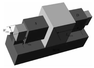
Fig. 1.
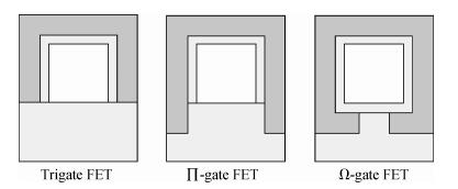
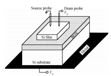
Structure of the traditional pseudo-MOS
SEMICONDUCTOR DEVICES
Shiyao Liu1, , Wei He1, Jianmin Cao1 and Siwen Huang1
Corresponding author: Liu Shiyao, Email:lewis_yao@163.com
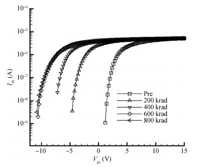
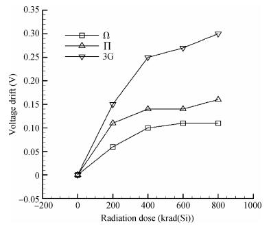
Abstract: This paper investigates the total ionizing dose response of different non-planar triple-gate transistor structures with different fin widths. By exposing the pseudo-MOS transistor to different amounts of radiation, different interface trap densities and trapped-oxide charges can be obtained. Using these parameters together with Altal 3D simulation software, the total dose radiation response of various non-planar triple-gate devices can be simulated. The behaviors of three kinds of non-planar devices are compared.
Key words: silicon-on-insulator, total ionizing dose effects, pseudo-MOS, non-planar triple-gate transistors
| [1] |
Rashkeev S N, Cirba C R, Fleetwood D M, et al. Physical model for enhanced interface-trap formation at low dose rates. IEEE Trans Nucl Sci, 2002, 49(6):26505 http://ieeexplore.ieee.org/document/1134199/authors
|
| [2] |
Chen X J, Barnaby H J, Vermeire B, et al. Mechanisms of enhanced radiation induced degradation due to excess molecular hydrogen in bipolar oxides. IEEE Trans Nucl Sci, 2007, 54(6):1993
|
| [3] |
Hjalmarson H P, Pease R L, Witczak S C, et al. Mechanisms for radiation dose-rate sensitivity of bipolar transistors. IEEE Trans Nucl Sci, 2003, 50(6):1901 doi: 10.1109/TNS.2003.821803
|
| [4] |
Wang T Q, Wei X D, Li H J, et al. Calculation of X-ray attenuation and energy deposition. Atomic Energy Science and Technology, 2007, 41(4):399(in Chinese)
|
| [5] |
Scofield J H, Fleetwood D M. Physical basis for nondestructive tests of MOS radiation hardness. IEEE Trans Nucl Sci, 1991, 38(6):1567 doi: 10.1109/23.124147
|
| [6] |
Yoshino A, Ma T P, Okumura K. Front-and back-interface trap densities and subthreshold swings of fully depleted mode metal-oxide-semiconductor transistors fabricated on separation-by-implanted-oxygen substrates. Jpn J Appl Phys, 1998, 37(7):3933
|
| [7] |
Gaillardin M, Paillet P, Ferlet-Cavrois V, et al. High tolerance to total ionizing dose of Ω -shaped gate field-effect transistors. Appl Phys Lett, 2006, 88(22):223511 doi: 10.1063/1.2206097
|
| [8] |
Gaillardin M, Paillet P, Ferlet-Cavrois V, et al. Total ionizing dose effects on triple-gate FETs. IEEE Trans Nucl Sci, 2006, 53(6):3158 doi: 10.1109/TNS.2006.884351
|
| [9] |
Daugé F, Pretet J, Cristoloveanu S, et al. Coupling effects and channels separation in FinFETs. Solid-State Electron, 2004, 48(4):535 doi: 10.1016/j.sse.2003.09.033
|
| [10] |
Ritzenthaler R, Cristoloveanu S, Faynot O, et al. Lateral coupling and immunity to substrate effect in FET devices. Solid State Electron, 2006, 50(3):558
|


Article views: 3248 Times PDF downloads: 14 Times Cited by: 0 Times
Received: 25 December 2012 Revised: 23 April 2013 Online: Published: 01 September 2013
| Citation: |
Shiyao Liu, Wei He, Jianmin Cao, Siwen Huang. The total ionizing dose effects of non-planar triple-gate transistors[J]. Journal of Semiconductors, 2013, 34(9): 094004. doi: 10.1088/1674-4926/34/9/094004
****
S Y Liu, W He, J M Cao, S W Huang. The total ionizing dose effects of non-planar triple-gate transistors[J]. J. Semicond., 2013, 34(9): 094004. doi: 10.1088/1674-4926/34/9/094004.

|
Project supported by the National Science Foundation for Young Scholars of China (No. 11105092) and the Shenzhen Science and Technology Development Funds (Nos. JC201005280565A, JC201005280558A, GJHS20120621142118853)
the Shenzhen Science and Technology Development Funds JC201005280565A
the National Science Foundation for Young Scholars of China 11105092
the Shenzhen Science and Technology Development Funds GJHS20120621142118853
the Shenzhen Science and Technology Development Funds JC201005280558A
| [1] |
Rashkeev S N, Cirba C R, Fleetwood D M, et al. Physical model for enhanced interface-trap formation at low dose rates. IEEE Trans Nucl Sci, 2002, 49(6):26505 http://ieeexplore.ieee.org/document/1134199/authors
|
| [2] |
Chen X J, Barnaby H J, Vermeire B, et al. Mechanisms of enhanced radiation induced degradation due to excess molecular hydrogen in bipolar oxides. IEEE Trans Nucl Sci, 2007, 54(6):1993
|
| [3] |
Hjalmarson H P, Pease R L, Witczak S C, et al. Mechanisms for radiation dose-rate sensitivity of bipolar transistors. IEEE Trans Nucl Sci, 2003, 50(6):1901 doi: 10.1109/TNS.2003.821803
|
| [4] |
Wang T Q, Wei X D, Li H J, et al. Calculation of X-ray attenuation and energy deposition. Atomic Energy Science and Technology, 2007, 41(4):399(in Chinese)
|
| [5] |
Scofield J H, Fleetwood D M. Physical basis for nondestructive tests of MOS radiation hardness. IEEE Trans Nucl Sci, 1991, 38(6):1567 doi: 10.1109/23.124147
|
| [6] |
Yoshino A, Ma T P, Okumura K. Front-and back-interface trap densities and subthreshold swings of fully depleted mode metal-oxide-semiconductor transistors fabricated on separation-by-implanted-oxygen substrates. Jpn J Appl Phys, 1998, 37(7):3933
|
| [7] |
Gaillardin M, Paillet P, Ferlet-Cavrois V, et al. High tolerance to total ionizing dose of Ω -shaped gate field-effect transistors. Appl Phys Lett, 2006, 88(22):223511 doi: 10.1063/1.2206097
|
| [8] |
Gaillardin M, Paillet P, Ferlet-Cavrois V, et al. Total ionizing dose effects on triple-gate FETs. IEEE Trans Nucl Sci, 2006, 53(6):3158 doi: 10.1109/TNS.2006.884351
|
| [9] |
Daugé F, Pretet J, Cristoloveanu S, et al. Coupling effects and channels separation in FinFETs. Solid-State Electron, 2004, 48(4):535 doi: 10.1016/j.sse.2003.09.033
|
| [10] |
Ritzenthaler R, Cristoloveanu S, Faynot O, et al. Lateral coupling and immunity to substrate effect in FET devices. Solid State Electron, 2006, 50(3):558
|

 WeChat ID
Journal of Semiconductors © 2017 All Rights Reserved 京ICP備05085259號-2
 DownLoad: