| [1] |
Xiang B, Zou T Y, Wang Y, et al. Photovoltage-coupled dual-gate InGaZnO thin-film transistors operated at the subthreshold region for low-power photodetection. ACS Appl Electron Mater, 2020, 2(6): 1745 doi: 10.1021/acsaelm.0c00308 |
| [2] |
Oommen R, Ganapathi Mavuri D S, Jose K, et al. Tunable memory behavior in light stimulated artificial synapse based on ZnO thin film transistors. J Phys D: Appl Phys, 2024, 57(46): 465102 doi: 10.1088/1361-6463/ad6dff |
| [3] |
Guo Y B, Zhu L Q. Recent progress in optoelectronic neuromorphic devices. Chin Phys B, 2020, 29(7): 078502 doi: 10.1088/1674-1056/ab99b6 |
| [4] |
Zhu X J, Lu W D. Optogenetics-inspired tunable synaptic functions in memristors. ACS Nano, 2018, 12(2): 1242 doi: 10.1021/acsnano.7b07317 |
| [5] |
Zhou L, Mao J Y, Ren Y, et al. Biological spiking synapse constructed from solution processed bimetal core-shell nanoparticle based composites. Small, 2018, 14(28): e1800288 doi: 10.1002/smll.201800288 |
| [6] |
Shi Z W, Wang W S, Ai L, et al. Non-associative learning behavior in mixed proton and electron conductor hybrid pseudo-diode. J Mater Sci Technol, 2023, 160: 204 doi: 10.1016/j.jmst.2023.02.061 |
| [7] |
Zhu J D, Yang Y C, Jia R D, et al. Ion gated synaptic transistors based on 2D van der waals crystals with tunable diffusive dynamics. Adv Mater, 2018, 30(21): e1800195 doi: 10.1002/adma.201800195 |
| [8] |
Yang R Q, Tian Y, Hu L X, et al. Dual-input optoelectronic synaptic transistor based on amorphous ZnAlSnO for multi-target neuromorphic simulation. Mater Today Nano, 2024, 26: 100480 doi: 10.1016/j.mtnano.2024.100480 |
| [9] |
Yang R Q, Hu D N, Chen Q J, et al. SnS-facilitated ZnAlSnO-based fully optically modulated artificial synaptic device for image processing. Adv Funct Mater, 2025, 35(4): 2414210 doi: 10.1002/adfm.202414210 |
| [10] |
Yang R Q, Wang Y, Li S Q, et al. All-optically controlled artificial synapse based on full oxides for low-power visible neural network computing. Adv Funct Mater, 2024, 34(10): 2312444 doi: 10.1002/adfm.202312444 |
| [11] |
Liang L Y, Zhang H B, Li T, et al. Addressing the conflict between mobility and stability in oxide thin-film transistors. Adv Sci, 2023, 10(14): e2300373. doi: 10.1002/advs.202300373 |
| [12] |
Shiah Y S, Sim K, Ueda S, et al. Unintended carbon-related impurity and negative bias instability in high-mobility oxide TFTs. IEEE Electron Device Lett, 2021, 42(9): 1319 doi: 10.1109/LED.2021.3101654 |
| [13] |
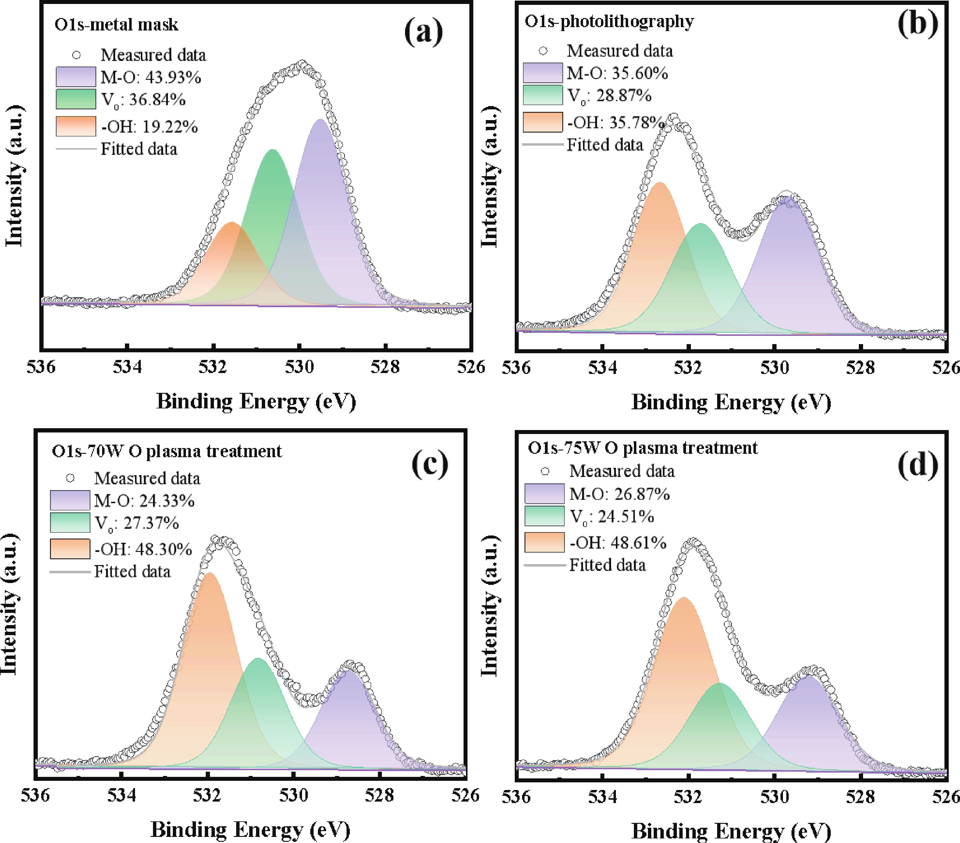
Xiao P, Huang J H, Dong T, et al. X-ray photoelectron spectroscopy analysis of the effect of photoresist passivation on InGaZnO thin-film transistors. Appl Surf Sci, 2019, 471: 403 doi: 10.1016/j.apsusc.2018.11.211 |
| [14] |
Shiah Y S, Sim K, Shi Y H, et al. Mobility–stability trade-off in oxide thin-film transistors. Nat Electron, 2021, 4: 800 doi: 10.1038/s41928-021-00671-0 |
| [15] |
Liu J S, He L F, Xu Z, et al. Defect generation mechanism in magnetron sputtered metal films on PMMA substrates. J Mater Sci Mater Electron, 2019, 30(16): 14847 doi: 10.1007/s10854-019-01855-3 |
| [16] |
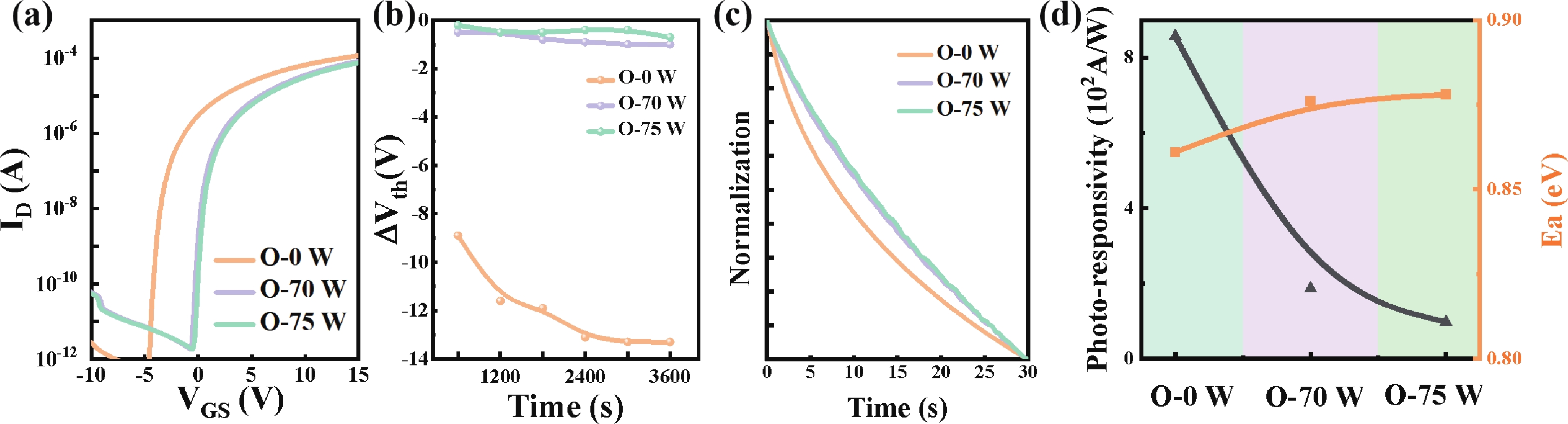
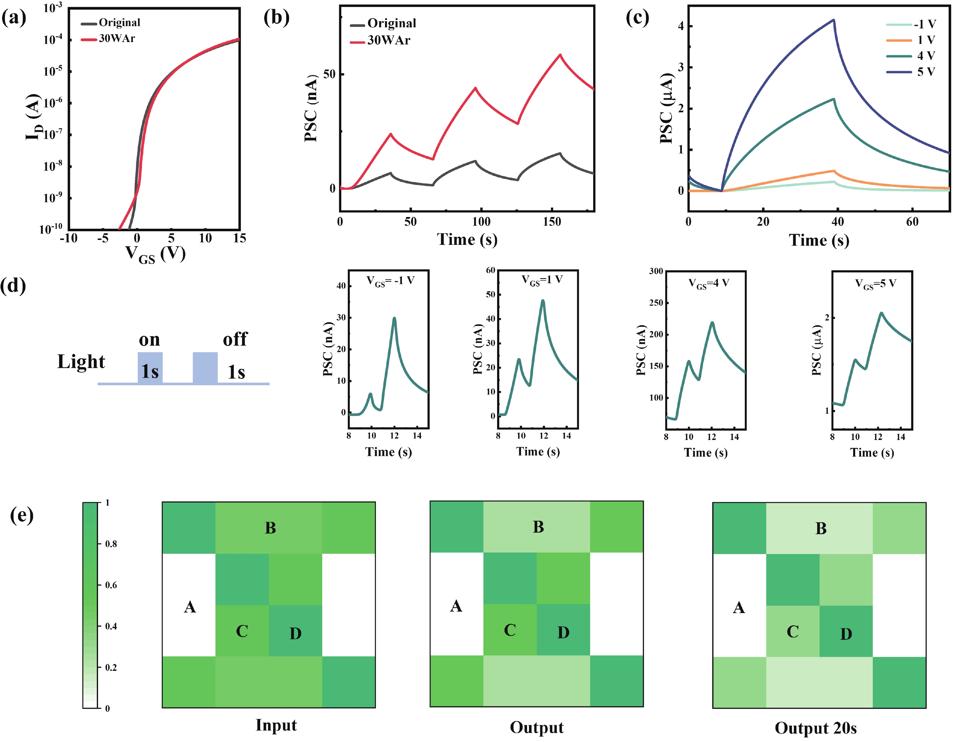
Lu J Q, Wang W H, Liang J X, et al. Contact resistance reduction of low temperature atomic layer deposition ZnO thin film transistor using Ar plasma surface treatment. IEEE Electron Device Lett, 2022, 43(6): 890 doi: 10.1109/LED.2022.3169345 |
| [17] |
Lee G W, Shim J I, Shin D S. On the ideality factor of the radiative recombination current in semiconductor light-emitting diodes. Appl Phys Lett, 2016, 109(3): 031104 doi: 10.1063/1.4959081 |
| [18] |
Goudon T, Miljanovi? V, Schmeiser C. On the Shockley–read–hall model: Generation-recombination in semiconductors. SIAM J Appl Math, 2007, 67(4): 1183 doi: 10.1137/060650751 |
| [19] |
Gao Z X, Ju X, Zhang H Z, et al. InP quantum dots tailored oxide thin film phototransistor for bioinspired visual adaptation. Adv Funct Mater, 2023, 33(52): 2305959 doi: 10.1002/adfm.202305959 |
| [20] |
Chen H Y, Ren J Y, Sun J T, et al. Photoresponse design in metal oxide semiconductor TFTs toward diverse applications: Display drivers, photodetectors, and optoelectronic synapses. ACS Appl Mater Interfaces, 2025, 17(5): 8727 doi: 10.1021/acsami.5c00152 |
| [21] |
Li T, Liu X H, Ren J Y, et al. High-mobility InSnZnO thin film transistors via introducing water vapor sputtering gas. ACS Appl Mater Interfaces, 2024, 16(24): 31237 doi: 10.1021/acsami.3c17894 |


 Jingting Sun received her BS in Materials Science and Engineering in 2018 from Yangtze Normal University and her MS degree in Materials Physics & Chemistry in 2025 from the University of Chinese Academy of Sciences (UCAS). She is currently conducting research on thin-film transistors (TFTs).
 Junyan Ren received her BS in Materials Chemistry in 2020 from Yunnan University and her MS/Ph.D degree in 2025 in Material Physics & Chemistry from Ningbo Institute of Materials Technology and Engineering (NIMTE), Chinese Academy of Sciences (CAS). She is currently a postdoctoral researcher at NIMTE, CAS. Her current research focuses on amorphous and nano-crystalline oxide semiconductors and their devices for electronics/optoelectronics.
 Lingyan Liang received her BS in physics in 2003 from Nanjing University and her MS/Ph.D degree in 2008 in Material Physics & Chemistry from Institute of Semiconductor, Chinese Academy of Sciences (CAS). She is currently a professor at Ningbo Institute of Material Technology and Engineering, CAS. Her current research focuses on amorphous and nano-crystalline oxide semiconductors and their devices for electronics/optoelectronics/bioelectronics.
 DownLoad: