Fig. 1.
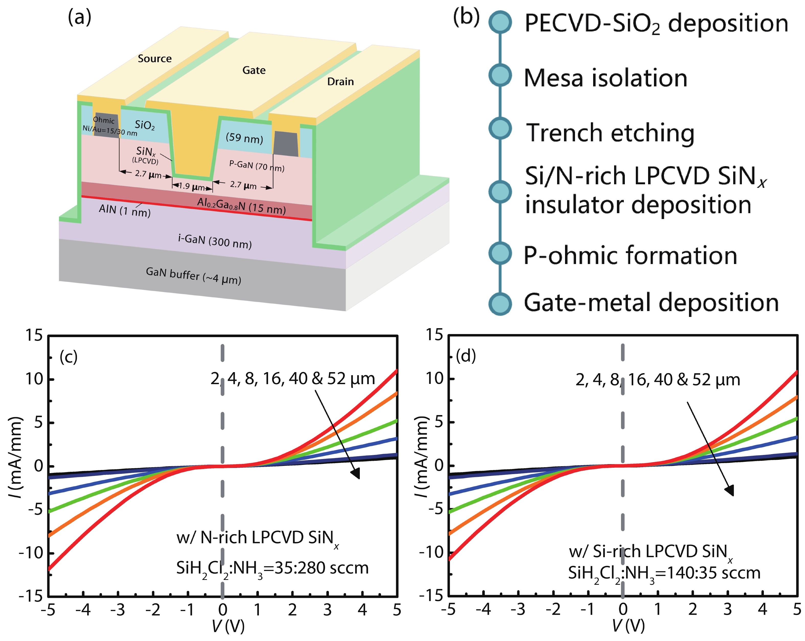
(Color online) (a) Epitaxial structure and schematic of the proposed device. (b) The fabrication procedure. The I–V characteristic measured from TLM for the samples with (c) N-rich LPCVD SiNx and (d) Si-rich LPCVD SiNx.
ARTICLES
Liyang Zhu1, Kuangli Chen1, Ying Ma2, Yong Cai2, Chunhua Zhou1, , Zhaoji Li1, Bo Zhang1 and Qi Zhou1, 3,
Corresponding author: Chunhua Zhou, czhou@uestc.edu.cn; Qi Zhou, zhouqi@uestc.edu.cn
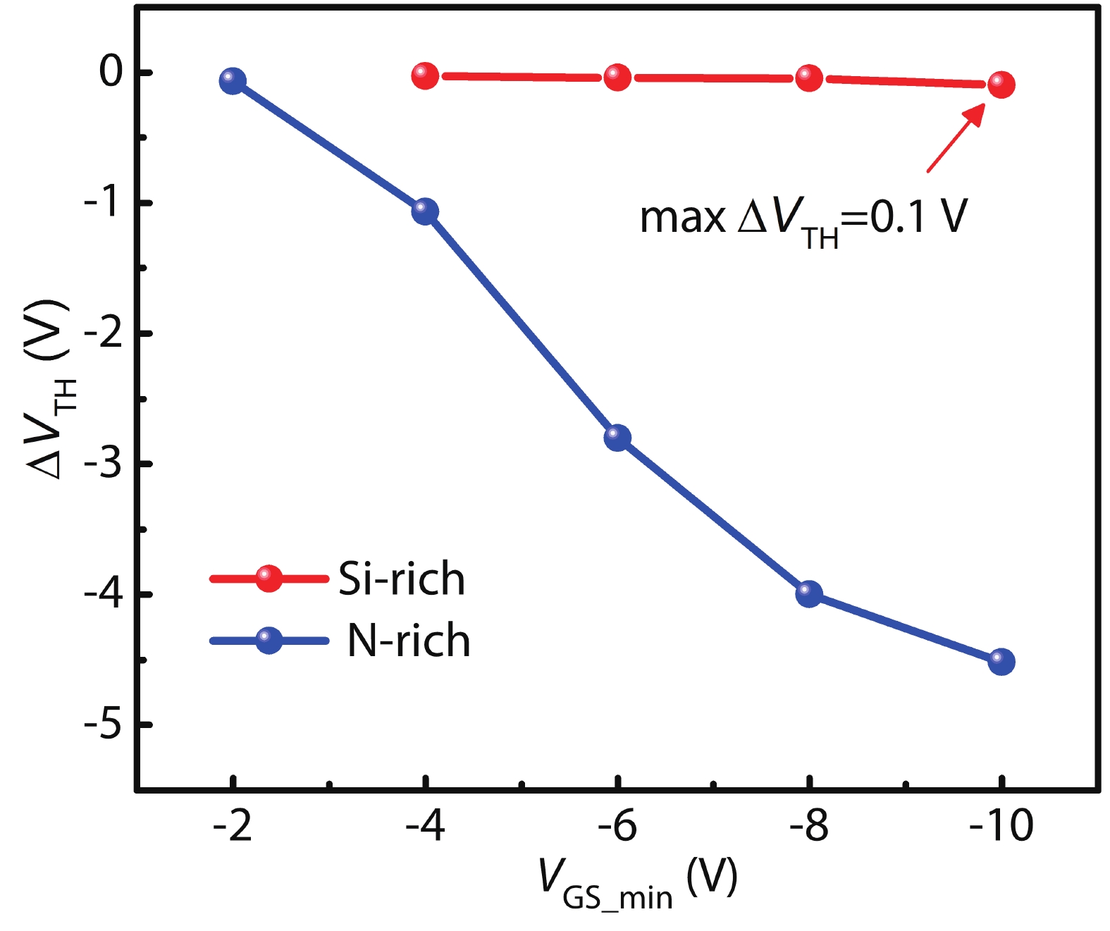
Abstract: In this work, the GaN p-MISFET with LPCVD-SiNx is studied as a gate dielectric to improve device performance. By changing the Si/N stoichiometry of SiNx, it is found that the channel hole mobility can be effectively enhanced with Si-rich SiNx gate dielectric, which leads to a respectably improved drive current of GaN p-FET. The record high channel mobility of 19.4 cm2/(V?s) was achieved in the device featuring an Enhancement-mode channel. Benefiting from the significantly improved channel mobility, the fabricated E-mode GaN p-MISFET is capable of delivering a decent-high current of 1.6 mA/mm, while simultaneously featuring a negative threshold-voltage (VTH) of –2.3 V (defining at a stringent criteria of 10 μA/mm). The device also exhibits a well pinch-off at 0 V with low leakage current of 1 nA/mm. This suggests that a decent E-mode operation of the fabricated p-FET is obtained. In addition, the VTH shows excellent stability, while the threshold-voltage hysteresis ΔVTH is as small as 0.1 V for a gate voltage swing up to –10 V, which is among the best results reported in the literature. The results indicate that optimizing the Si/N stoichiometry of LPCVD-SiNx is a promising approach to improve the device performance of GaN p-MISFET.
Key words: p-channel, GaN p-FET, LPCVD, channel mobility, hole mobility, enhancement-mode
| [1] |
Teo K H, Zhang Y H, Chowdhury N, et al. Emerging GaN technologies for power, RF, digital, and quantum computing applications: Recent advances and prospects. J Appl Phys, 2021, 130, 160902 doi: 10.1063/5.0061555
|
| [2] |
Amano H, Baines Y, Beam E, et al. The 2018 GaN power electronics roadmap. J Phys D: Appl Phys, 2018, 51, 163001 doi: 10.1088/1361-6463/aaaf9d
|
| [3] |
Trescases O, Murray S K, Jiang W L, et al. GaN power ICs: Reviewing strengths, gaps, and future directions. 2020 IEEE International Electron Devices Meeting (IEDM), 2021, 27.4.1 doi: 10.1109/IEDM13553.2020.9371918
|
| [4] |
Dan K. Monolithic GaN power IC technology drives wide bandgap adoption. 2020 IEEE International Electron Devices Meeting (IEDM), 2021, 27.5.1 doi: 10.1109/IEDM13553.2020.9372021
|
| [5] |
Hahn H, Reuters B, Kotzea S, et al. First monolithic integration of GaN-based enhancement mode n-channel and p-channel heterostructure field effect transistors. 72nd Device Research Conference, 2014, 259 doi: 10.1109/DRC.2014.6872396
|
| [6] |
Nakajima A, Nishizawa S I, Ohashi H, et al. One-chip operation of GaN-based P-channel and N-channel heterojunction field effect transistors. 2014 IEEE 26th International Symposium on Power Semiconductor Devices & IC's (ISPSD), 2014, 241 doi: 10.1109/ISPSD.2014.6856021
|
| [7] |
Zheng Z Y, Zhang L, Song W J, et al. Gallium nitride-based complementary logic integrated circuits. Nat Electron, 2021, 4, 595 doi: 10.1038/s41928-021-00611-y
|
| [8] |
Niu X R, Hou B, Yang L, et al. Analytical model on the threshold voltage of p-channel heterostructure field-effect transistors on a GaN-based complementary circuit platform. IEEE Trans Electron Devices, 2022, 69, 57 doi: 10.1109/TED.2021.3129712
|
| [9] |
Raj A, Krishna A, Hatui N, et al. Demonstration of a GaN/AlGaN superlattice-based p-channel FinFET with high ON-current. IEEE Electron Device Lett, 2020, 41, 220 doi: 10.1109/LED.2019.2963428
|
| [10] |
Bader S J, Chaudhuri R, Nomoto K, et al. Gate-recessed E-mode p-channel HFET with high on-current based on GaN/AlN 2D hole gas. IEEE Electron Device Lett, 2018, 39, 1848 doi: 10.1109/LED.2018.2874190
|
| [11] |
Raj A, Krishna A, Hatui N, et al. GaN/AlGaN superlattice based E-mode p-channel MES-FinFET with regrown contacts and >50 mA/mm on-current. 2021 IEEE International Electron Devices Meeting (IEDM), 2022, 5.4.1 doi: 10.1109/IEDM19574.2021.9720496
|
| [12] |
Chowdhury N, Xie Q Y, Palacios T. Tungsten-gated GaN/AlGaN p-FET with Imax > 120 mA/mm on GaN-on-Si. IEEE Electron Device Lett, 2022, 43, 545 doi: 10.1109/LED.2022.3149659
|
| [13] |
Chowdhury N, Xie Q Y, Palacios T. Self-aligned E-mode GaN p-channel FinFET with ION > 100 mA/mm and ION/IOFF > 107. IEEE Electron Device Lett, 2022, 43, 358 doi: 10.1109/LED.2022.3140281
|
| [14] |
Du H H, Liu Z H, Hao L, et al. High-performance E-mode p-channel GaN FinFET on silicon substrate with high ION/IOFF and high threshold voltage. IEEE Electron Device Lett, 2022, 43, 705 doi: 10.1109/LED.2022.3155152
|
| [15] |
Zheng Z Y, Song W J, Zhang L, et al. High ION and ION/IOFF ratio enhancement?mode buried ratio enhancement?mode buried p-channel GaN MOSFETs on p-GaN gate power HEMT platform. IEEE Electron Device Lett, 2020, 41, 26 doi: 10.1109/LED.2019.2954035
|
| [16] |
Yin Y D, Lee K B. High-performance enhancement-mode p-channel GaN MISFETs with steep subthreshold swing. IEEE Electron Device Lett, 2022, 43, 533 doi: 10.1109/LED.2022.3152308
|
| [17] |
Chowdhury N, Lemettinen J, Xie Q Y, et al. P-channel GaN transistor based on p-GaN/AlGaN/GaN on Si. IEEE Electron Device Lett, 2019, 40, 1036 doi: 10.1109/LED.2019.2916253
|
| [18] |
Chowdhury N, Xie Q Y, Yuan M Y, et al. Regrowth-free GaN-based complementary logic on a Si substrate. IEEE Electron Device Lett, 2020, 41, 820 doi: 10.1109/LED.2020.2987003
|
| [19] |
Schroder D K. Semiconductor material and device characterization. Wiley-IEEE Press, 2005
|
| [20] |
Makino T. Composition and structure control by source gas ratio in LPCVD SiNx. J Electrochem Soc, 1983, 130, 450 doi: 10.1149/1.2119729
|
| [21] |
Zhu L Y, Zhou Q, Chen K L, et al. The modulation effect of LPCVD-SixNy stoichiometry on 2-DEG characteristic of UTB AlGaN/GaN heterostructure. IEEE Trans Electron Devices, 2022, 69, 4828 doi: 10.1109/TED.2022.3188609
|
| [22] |
Jin H, Jiang Q M, Huang S, et al. An enhancement-mode GaN p-FET with improved breakdown voltage. IEEE Electron Device Lett, 2022, 43, 1191 doi: 10.1109/LED.2022.3184998
|
| [23] |
Zheng Z Y, Zhang L, Song W J, et al. Threshold voltage instability of enhancement-mode GaN buried p-channel MOSFETs. IEEE Electron Device Lett, 2021, 42, 1584 doi: 10.1109/LED.2021.3114776
|
| [24] |
Zhang L, Zheng Z Y, Cheng Y, et al. SiN/in-situ-GaON staggered gate stack on p-GaN for enhanced stability in buried-channel GaN p-FETs. 2021 IEEE International Electron Devices Meeting (IEDM), 2022, 5.3.1 doi: 10.1109/IEDM19574.2021.9720653
|
| [25] |
Poncé S, Jena D, Giustino F. Hole mobility of strained GaN from first principles. Phys Rev B, 2019, 100, 085204 doi: 10.1103/PhysRevB.100.085204
|
| [26] |
Siddique A, Ahmed R, Anderson J, et al. Effect of reactant gas stoichiometry of in-situ SiNx passivation on structural properties of MOCVD AlGaN/GaN HEMTs. J Cryst Growth, 2019, 517, 28 doi: 10.1016/j.jcrysgro.2019.03.020
|
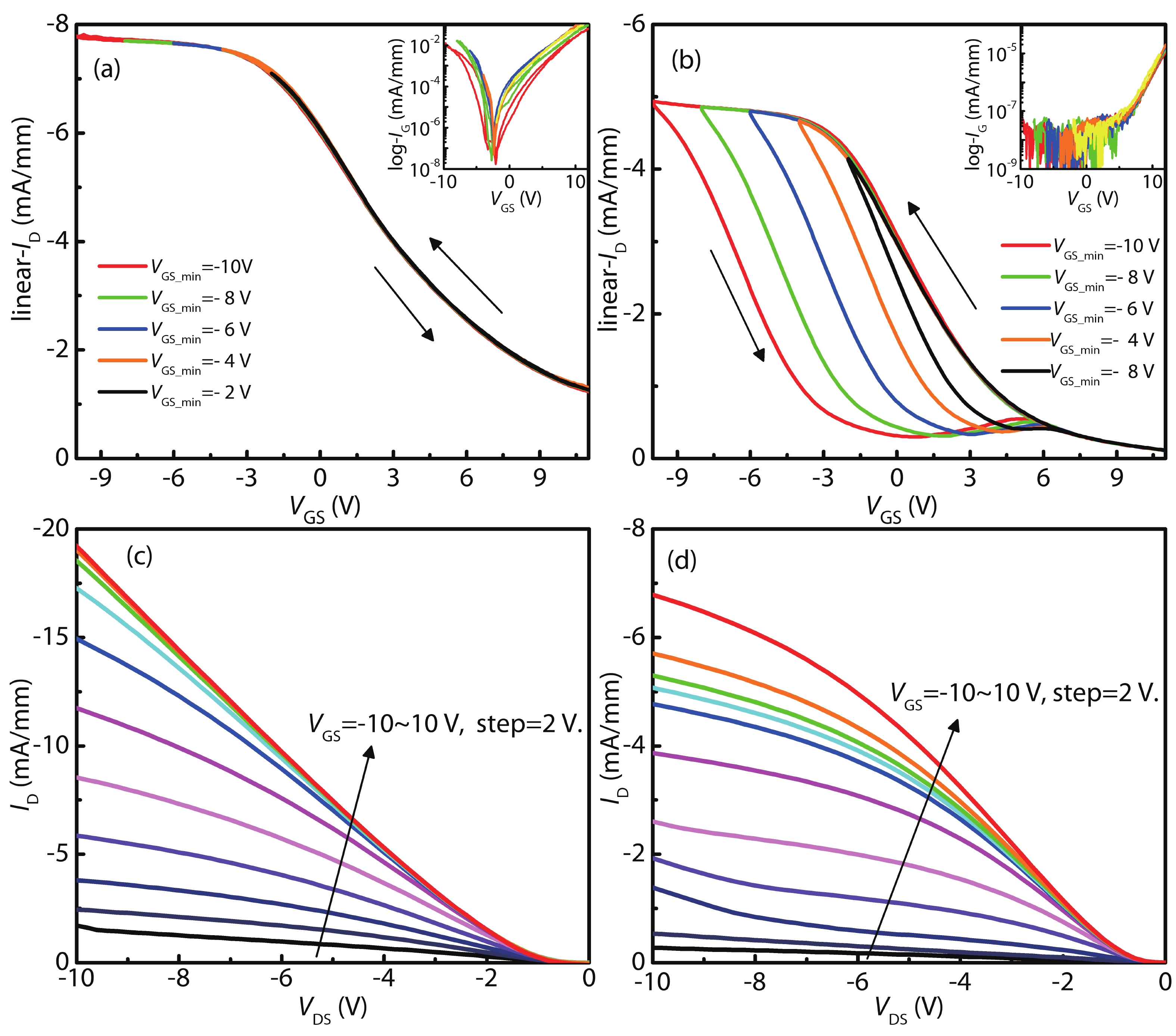
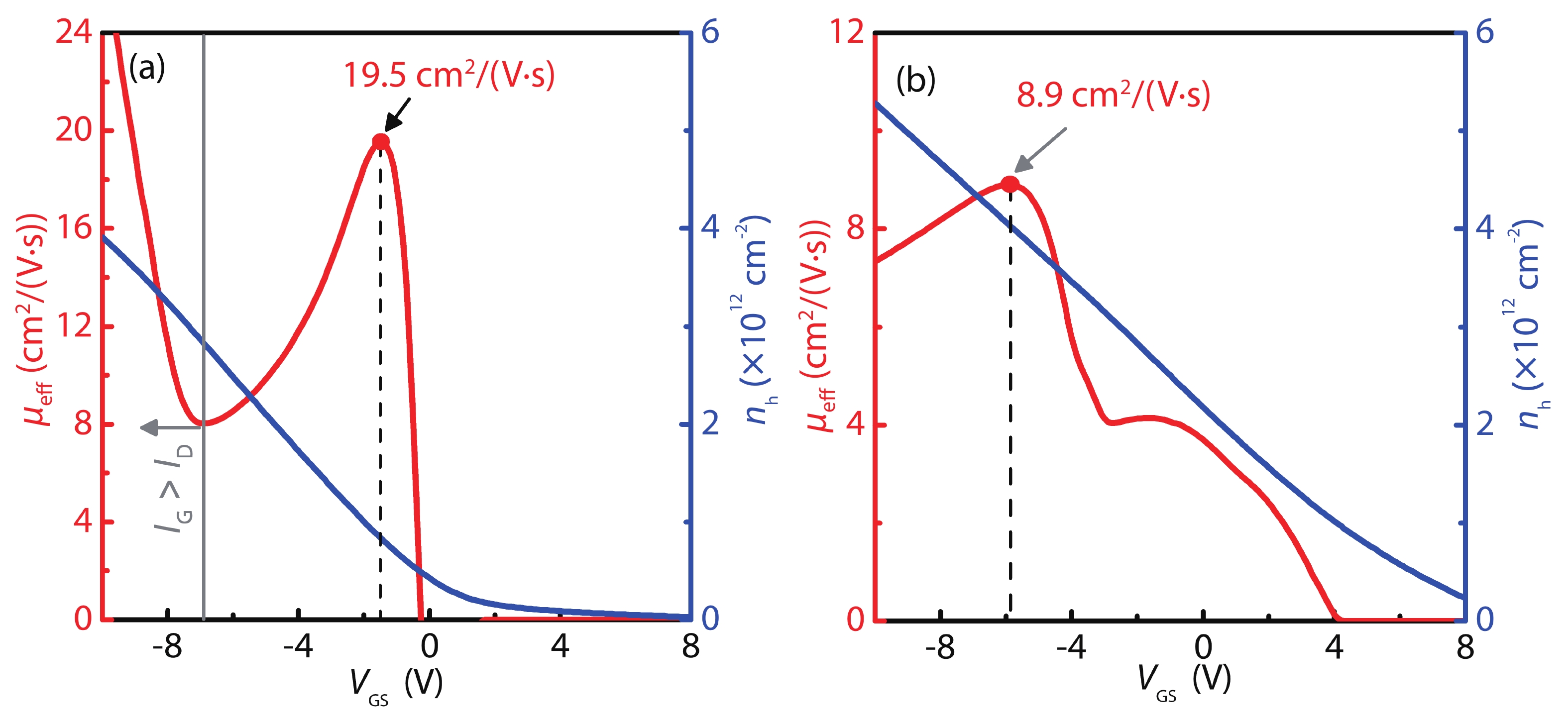
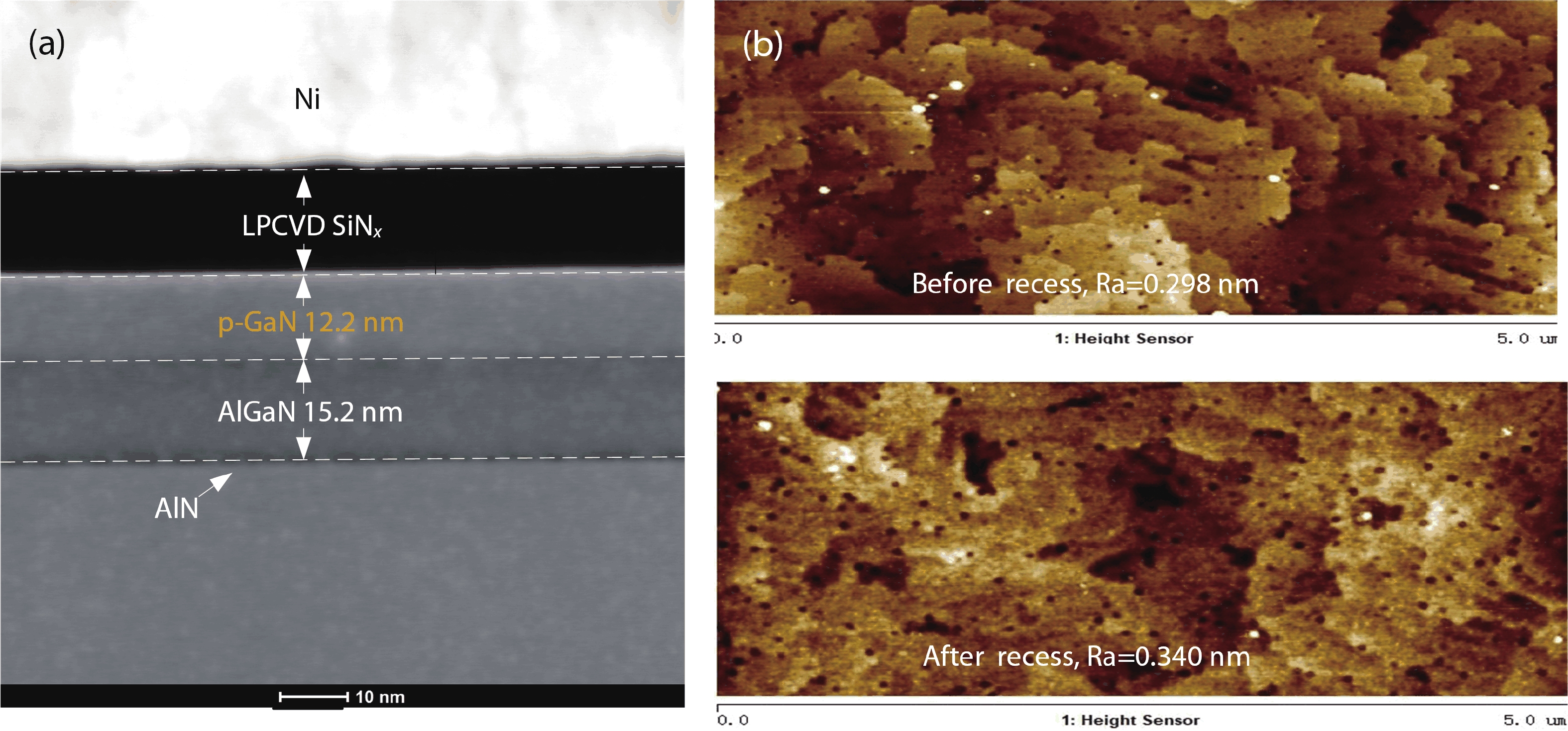
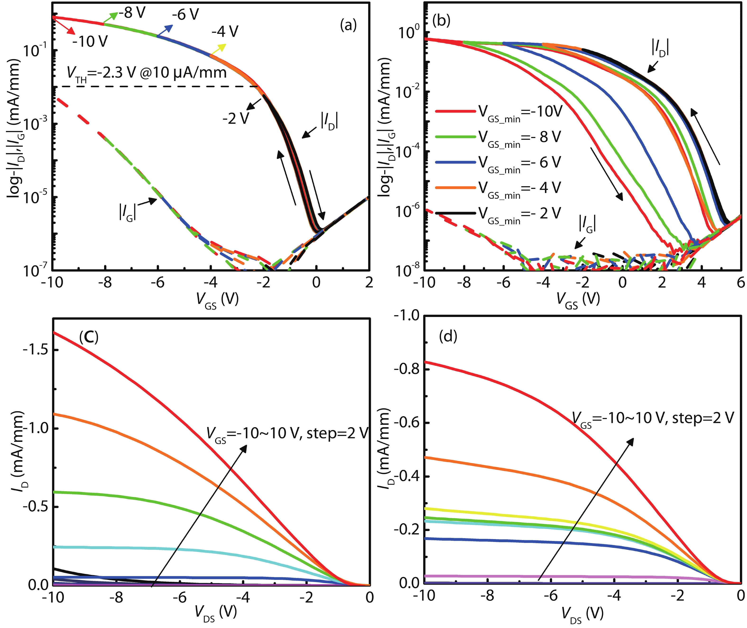
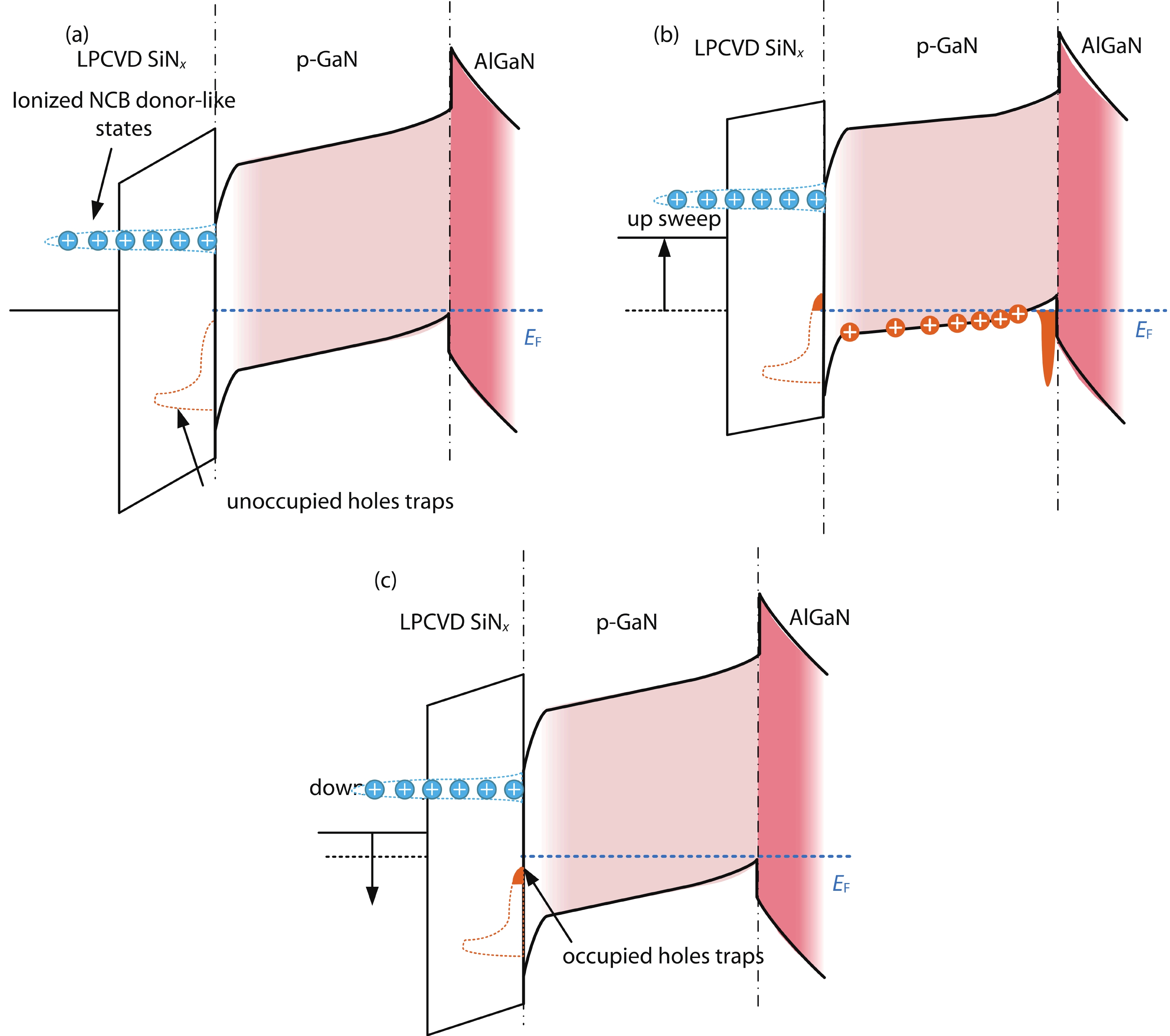
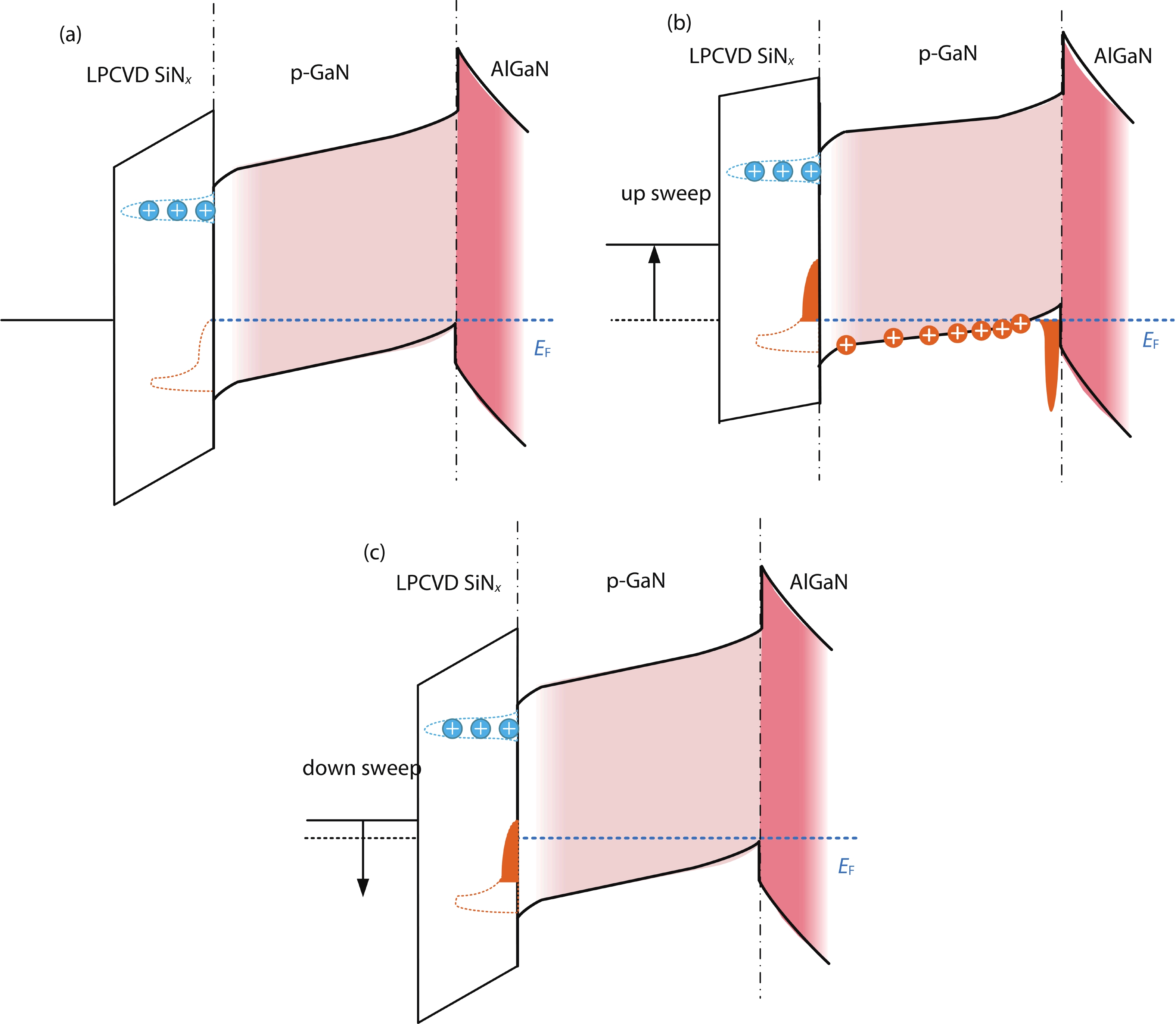
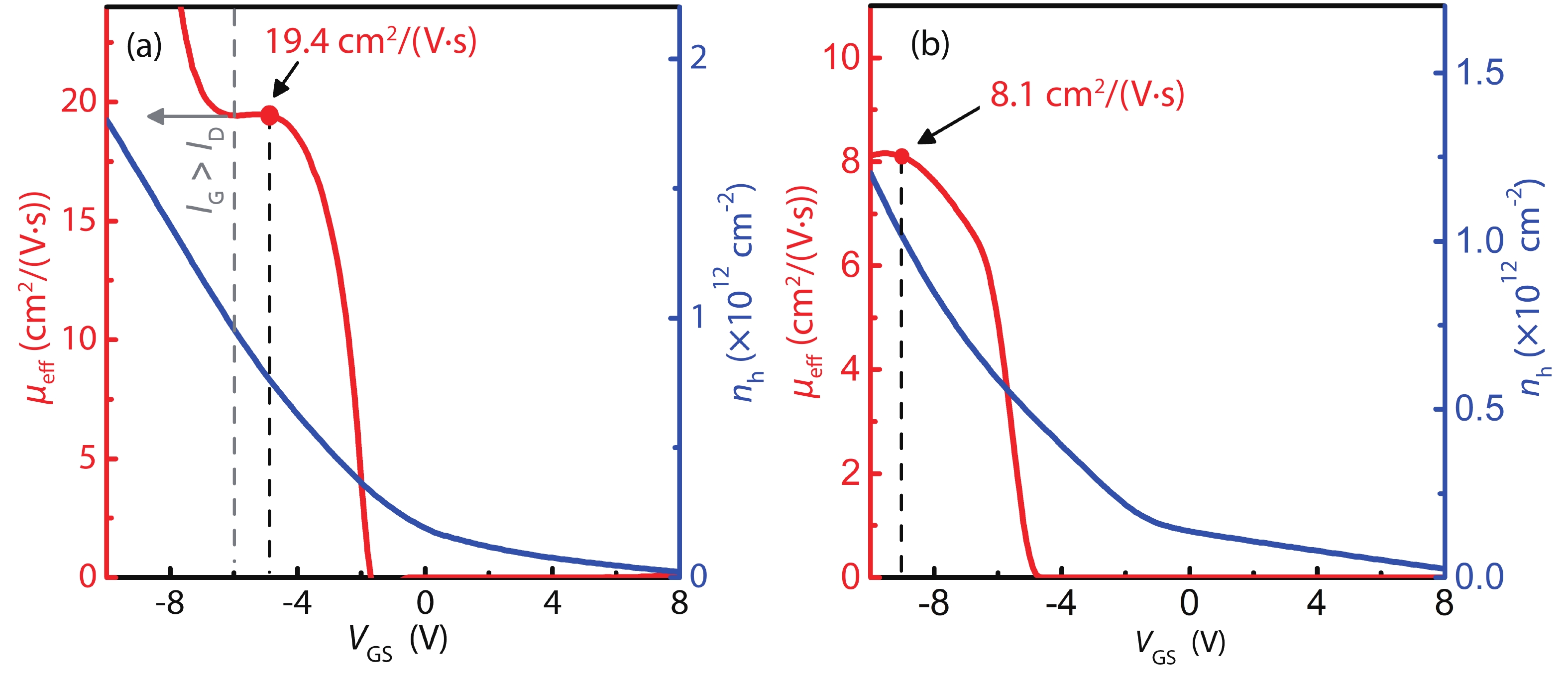
Table 1. Benchmark of typical parameters of GaN p-FETs.
| Group | Mobility (cm2/(V?s)) | ION/IOFF f | VTH (V) | ΔVTH (V@VGS_min) | RON (kΩ?mm) |
| This work | 19.4a | 5×10⁵ | ?2.3c | ?0.1 (@-10 V) | 5.7 |
| Xidian[14] | 2b | ~102 | ?2.2d | N. A. | 0.54 |
| Sheffield[16] | 11.8a | ~107 | ?0.73c | ?0.12 (@?8 V) | 1 |
| HKUST[24] | N. A.e | ~2×10⁷ | ?1.7c | ~?0.1 (@?6 V) | 0.65 |
| SINANO[22] | 11b | ~106 | ?2.7c | ?2.4 (@?12 V) | 0.061 |
| MIT[12] | 15b | ~10 | 3.5d | N. A. | 2.3 |
| MIT[13] | 11b | ~10 | ?0.3d | N. A. | 2.3 |
| MIT[18] | 10a | ~102 | ?1 | N. A. | 2.4 |
| MIT[17] | 7.5a | ~106 | 2 | N. A. | |
| HKUST[15] | 10.2b | ~2×10⁷ | ?1.7c | N. A. | |
| a mobility in channel; b mobility in access region; c defined at ID = 0.01 mA/mm; d defined by linear-extrapolation; e N. A. is abbreviation for “not available”; f IOFF in here was the current when VGS is biased to 0 V. | |||||
 DownLoad: CSV
| [1] |
Teo K H, Zhang Y H, Chowdhury N, et al. Emerging GaN technologies for power, RF, digital, and quantum computing applications: Recent advances and prospects. J Appl Phys, 2021, 130, 160902 doi: 10.1063/5.0061555
|
| [2] |
Amano H, Baines Y, Beam E, et al. The 2018 GaN power electronics roadmap. J Phys D: Appl Phys, 2018, 51, 163001 doi: 10.1088/1361-6463/aaaf9d
|
| [3] |
Trescases O, Murray S K, Jiang W L, et al. GaN power ICs: Reviewing strengths, gaps, and future directions. 2020 IEEE International Electron Devices Meeting (IEDM), 2021, 27.4.1 doi: 10.1109/IEDM13553.2020.9371918
|
| [4] |
Dan K. Monolithic GaN power IC technology drives wide bandgap adoption. 2020 IEEE International Electron Devices Meeting (IEDM), 2021, 27.5.1 doi: 10.1109/IEDM13553.2020.9372021
|
| [5] |
Hahn H, Reuters B, Kotzea S, et al. First monolithic integration of GaN-based enhancement mode n-channel and p-channel heterostructure field effect transistors. 72nd Device Research Conference, 2014, 259 doi: 10.1109/DRC.2014.6872396
|
| [6] |
Nakajima A, Nishizawa S I, Ohashi H, et al. One-chip operation of GaN-based P-channel and N-channel heterojunction field effect transistors. 2014 IEEE 26th International Symposium on Power Semiconductor Devices & IC's (ISPSD), 2014, 241 doi: 10.1109/ISPSD.2014.6856021
|
| [7] |
Zheng Z Y, Zhang L, Song W J, et al. Gallium nitride-based complementary logic integrated circuits. Nat Electron, 2021, 4, 595 doi: 10.1038/s41928-021-00611-y
|
| [8] |
Niu X R, Hou B, Yang L, et al. Analytical model on the threshold voltage of p-channel heterostructure field-effect transistors on a GaN-based complementary circuit platform. IEEE Trans Electron Devices, 2022, 69, 57 doi: 10.1109/TED.2021.3129712
|
| [9] |
Raj A, Krishna A, Hatui N, et al. Demonstration of a GaN/AlGaN superlattice-based p-channel FinFET with high ON-current. IEEE Electron Device Lett, 2020, 41, 220 doi: 10.1109/LED.2019.2963428
|
| [10] |
Bader S J, Chaudhuri R, Nomoto K, et al. Gate-recessed E-mode p-channel HFET with high on-current based on GaN/AlN 2D hole gas. IEEE Electron Device Lett, 2018, 39, 1848 doi: 10.1109/LED.2018.2874190
|
| [11] |
Raj A, Krishna A, Hatui N, et al. GaN/AlGaN superlattice based E-mode p-channel MES-FinFET with regrown contacts and >50 mA/mm on-current. 2021 IEEE International Electron Devices Meeting (IEDM), 2022, 5.4.1 doi: 10.1109/IEDM19574.2021.9720496
|
| [12] |
Chowdhury N, Xie Q Y, Palacios T. Tungsten-gated GaN/AlGaN p-FET with Imax > 120 mA/mm on GaN-on-Si. IEEE Electron Device Lett, 2022, 43, 545 doi: 10.1109/LED.2022.3149659
|
| [13] |
Chowdhury N, Xie Q Y, Palacios T. Self-aligned E-mode GaN p-channel FinFET with ION > 100 mA/mm and ION/IOFF > 107. IEEE Electron Device Lett, 2022, 43, 358 doi: 10.1109/LED.2022.3140281
|
| [14] |
Du H H, Liu Z H, Hao L, et al. High-performance E-mode p-channel GaN FinFET on silicon substrate with high ION/IOFF and high threshold voltage. IEEE Electron Device Lett, 2022, 43, 705 doi: 10.1109/LED.2022.3155152
|
| [15] |
Zheng Z Y, Song W J, Zhang L, et al. High ION and ION/IOFF ratio enhancement?mode buried ratio enhancement?mode buried p-channel GaN MOSFETs on p-GaN gate power HEMT platform. IEEE Electron Device Lett, 2020, 41, 26 doi: 10.1109/LED.2019.2954035
|
| [16] |
Yin Y D, Lee K B. High-performance enhancement-mode p-channel GaN MISFETs with steep subthreshold swing. IEEE Electron Device Lett, 2022, 43, 533 doi: 10.1109/LED.2022.3152308
|
| [17] |
Chowdhury N, Lemettinen J, Xie Q Y, et al. P-channel GaN transistor based on p-GaN/AlGaN/GaN on Si. IEEE Electron Device Lett, 2019, 40, 1036 doi: 10.1109/LED.2019.2916253
|
| [18] |
Chowdhury N, Xie Q Y, Yuan M Y, et al. Regrowth-free GaN-based complementary logic on a Si substrate. IEEE Electron Device Lett, 2020, 41, 820 doi: 10.1109/LED.2020.2987003
|
| [19] |
Schroder D K. Semiconductor material and device characterization. Wiley-IEEE Press, 2005
|
| [20] |
Makino T. Composition and structure control by source gas ratio in LPCVD SiNx. J Electrochem Soc, 1983, 130, 450 doi: 10.1149/1.2119729
|
| [21] |
Zhu L Y, Zhou Q, Chen K L, et al. The modulation effect of LPCVD-SixNy stoichiometry on 2-DEG characteristic of UTB AlGaN/GaN heterostructure. IEEE Trans Electron Devices, 2022, 69, 4828 doi: 10.1109/TED.2022.3188609
|
| [22] |
Jin H, Jiang Q M, Huang S, et al. An enhancement-mode GaN p-FET with improved breakdown voltage. IEEE Electron Device Lett, 2022, 43, 1191 doi: 10.1109/LED.2022.3184998
|
| [23] |
Zheng Z Y, Zhang L, Song W J, et al. Threshold voltage instability of enhancement-mode GaN buried p-channel MOSFETs. IEEE Electron Device Lett, 2021, 42, 1584 doi: 10.1109/LED.2021.3114776
|
| [24] |
Zhang L, Zheng Z Y, Cheng Y, et al. SiN/in-situ-GaON staggered gate stack on p-GaN for enhanced stability in buried-channel GaN p-FETs. 2021 IEEE International Electron Devices Meeting (IEDM), 2022, 5.3.1 doi: 10.1109/IEDM19574.2021.9720653
|
| [25] |
Poncé S, Jena D, Giustino F. Hole mobility of strained GaN from first principles. Phys Rev B, 2019, 100, 085204 doi: 10.1103/PhysRevB.100.085204
|
| [26] |
Siddique A, Ahmed R, Anderson J, et al. Effect of reactant gas stoichiometry of in-situ SiNx passivation on structural properties of MOCVD AlGaN/GaN HEMTs. J Cryst Growth, 2019, 517, 28 doi: 10.1016/j.jcrysgro.2019.03.020
|


Article views: 2523 Times PDF downloads: 220 Times Cited by: 0 Times
Received: 14 January 2023 Revised: 12 February 2023 Online: Accepted Manuscript: 30 March 2023Uncorrected proof: 06 April 2023Corrected proof: 13 July 2023Published: 10 August 2023
| Citation: |
Liyang Zhu, Kuangli Chen, Ying Ma, Yong Cai, Chunhua Zhou, Zhaoji Li, Bo Zhang, Qi Zhou. High threshold voltage enhancement-mode GaN p-FET with Si-rich LPCVD SiNx gate insulator for high hole mobility[J]. Journal of Semiconductors, 2023, 44(8): 082801. doi: 10.1088/1674-4926/44/8/082801
****
L Y Zhu, K L Chen, Y Ma, Y Cai, C H Zhou, Z J Li, B Zhang, Q Zhou. High threshold voltage enhancement-mode GaN p-FET with Si-rich LPCVD SiNx gate insulator for high hole mobility[J]. J. Semicond, 2023, 44(8): 082801. doi: 10.1088/1674-4926/44/8/082801

|
 Liyang Zhu:received his B.S. degree from the University of Electronic Science and Technology of China, Chengdu, China, in 2016. He is currently a doctoral candidate with the University of Electronic Science and Technology of China, Chengdu, China
 Qi Zhou:received his Ph.D. degree in electronic and computer engineering from the Hong Kong University of Science and Technology, Hong Kong, in 2012. He is currently a professor with the University of Electronic Science and Technology of China, Chengdu, China
| [1] |
Teo K H, Zhang Y H, Chowdhury N, et al. Emerging GaN technologies for power, RF, digital, and quantum computing applications: Recent advances and prospects. J Appl Phys, 2021, 130, 160902 doi: 10.1063/5.0061555
|
| [2] |
Amano H, Baines Y, Beam E, et al. The 2018 GaN power electronics roadmap. J Phys D: Appl Phys, 2018, 51, 163001 doi: 10.1088/1361-6463/aaaf9d
|
| [3] |
Trescases O, Murray S K, Jiang W L, et al. GaN power ICs: Reviewing strengths, gaps, and future directions. 2020 IEEE International Electron Devices Meeting (IEDM), 2021, 27.4.1 doi: 10.1109/IEDM13553.2020.9371918
|
| [4] |
Dan K. Monolithic GaN power IC technology drives wide bandgap adoption. 2020 IEEE International Electron Devices Meeting (IEDM), 2021, 27.5.1 doi: 10.1109/IEDM13553.2020.9372021
|
| [5] |
Hahn H, Reuters B, Kotzea S, et al. First monolithic integration of GaN-based enhancement mode n-channel and p-channel heterostructure field effect transistors. 72nd Device Research Conference, 2014, 259 doi: 10.1109/DRC.2014.6872396
|
| [6] |
Nakajima A, Nishizawa S I, Ohashi H, et al. One-chip operation of GaN-based P-channel and N-channel heterojunction field effect transistors. 2014 IEEE 26th International Symposium on Power Semiconductor Devices & IC's (ISPSD), 2014, 241 doi: 10.1109/ISPSD.2014.6856021
|
| [7] |
Zheng Z Y, Zhang L, Song W J, et al. Gallium nitride-based complementary logic integrated circuits. Nat Electron, 2021, 4, 595 doi: 10.1038/s41928-021-00611-y
|
| [8] |
Niu X R, Hou B, Yang L, et al. Analytical model on the threshold voltage of p-channel heterostructure field-effect transistors on a GaN-based complementary circuit platform. IEEE Trans Electron Devices, 2022, 69, 57 doi: 10.1109/TED.2021.3129712
|
| [9] |
Raj A, Krishna A, Hatui N, et al. Demonstration of a GaN/AlGaN superlattice-based p-channel FinFET with high ON-current. IEEE Electron Device Lett, 2020, 41, 220 doi: 10.1109/LED.2019.2963428
|
| [10] |
Bader S J, Chaudhuri R, Nomoto K, et al. Gate-recessed E-mode p-channel HFET with high on-current based on GaN/AlN 2D hole gas. IEEE Electron Device Lett, 2018, 39, 1848 doi: 10.1109/LED.2018.2874190
|
| [11] |
Raj A, Krishna A, Hatui N, et al. GaN/AlGaN superlattice based E-mode p-channel MES-FinFET with regrown contacts and >50 mA/mm on-current. 2021 IEEE International Electron Devices Meeting (IEDM), 2022, 5.4.1 doi: 10.1109/IEDM19574.2021.9720496
|
| [12] |
Chowdhury N, Xie Q Y, Palacios T. Tungsten-gated GaN/AlGaN p-FET with Imax > 120 mA/mm on GaN-on-Si. IEEE Electron Device Lett, 2022, 43, 545 doi: 10.1109/LED.2022.3149659
|
| [13] |
Chowdhury N, Xie Q Y, Palacios T. Self-aligned E-mode GaN p-channel FinFET with ION > 100 mA/mm and ION/IOFF > 107. IEEE Electron Device Lett, 2022, 43, 358 doi: 10.1109/LED.2022.3140281
|
| [14] |
Du H H, Liu Z H, Hao L, et al. High-performance E-mode p-channel GaN FinFET on silicon substrate with high ION/IOFF and high threshold voltage. IEEE Electron Device Lett, 2022, 43, 705 doi: 10.1109/LED.2022.3155152
|
| [15] |
Zheng Z Y, Song W J, Zhang L, et al. High ION and ION/IOFF ratio enhancement?mode buried ratio enhancement?mode buried p-channel GaN MOSFETs on p-GaN gate power HEMT platform. IEEE Electron Device Lett, 2020, 41, 26 doi: 10.1109/LED.2019.2954035
|
| [16] |
Yin Y D, Lee K B. High-performance enhancement-mode p-channel GaN MISFETs with steep subthreshold swing. IEEE Electron Device Lett, 2022, 43, 533 doi: 10.1109/LED.2022.3152308
|
| [17] |
Chowdhury N, Lemettinen J, Xie Q Y, et al. P-channel GaN transistor based on p-GaN/AlGaN/GaN on Si. IEEE Electron Device Lett, 2019, 40, 1036 doi: 10.1109/LED.2019.2916253
|
| [18] |
Chowdhury N, Xie Q Y, Yuan M Y, et al. Regrowth-free GaN-based complementary logic on a Si substrate. IEEE Electron Device Lett, 2020, 41, 820 doi: 10.1109/LED.2020.2987003
|
| [19] |
Schroder D K. Semiconductor material and device characterization. Wiley-IEEE Press, 2005
|
| [20] |
Makino T. Composition and structure control by source gas ratio in LPCVD SiNx. J Electrochem Soc, 1983, 130, 450 doi: 10.1149/1.2119729
|
| [21] |
Zhu L Y, Zhou Q, Chen K L, et al. The modulation effect of LPCVD-SixNy stoichiometry on 2-DEG characteristic of UTB AlGaN/GaN heterostructure. IEEE Trans Electron Devices, 2022, 69, 4828 doi: 10.1109/TED.2022.3188609
|
| [22] |
Jin H, Jiang Q M, Huang S, et al. An enhancement-mode GaN p-FET with improved breakdown voltage. IEEE Electron Device Lett, 2022, 43, 1191 doi: 10.1109/LED.2022.3184998
|
| [23] |
Zheng Z Y, Zhang L, Song W J, et al. Threshold voltage instability of enhancement-mode GaN buried p-channel MOSFETs. IEEE Electron Device Lett, 2021, 42, 1584 doi: 10.1109/LED.2021.3114776
|
| [24] |
Zhang L, Zheng Z Y, Cheng Y, et al. SiN/in-situ-GaON staggered gate stack on p-GaN for enhanced stability in buried-channel GaN p-FETs. 2021 IEEE International Electron Devices Meeting (IEDM), 2022, 5.3.1 doi: 10.1109/IEDM19574.2021.9720653
|
| [25] |
Poncé S, Jena D, Giustino F. Hole mobility of strained GaN from first principles. Phys Rev B, 2019, 100, 085204 doi: 10.1103/PhysRevB.100.085204
|
| [26] |
Siddique A, Ahmed R, Anderson J, et al. Effect of reactant gas stoichiometry of in-situ SiNx passivation on structural properties of MOCVD AlGaN/GaN HEMTs. J Cryst Growth, 2019, 517, 28 doi: 10.1016/j.jcrysgro.2019.03.020
|

 WeChat ID
Journal of Semiconductors © 2017 All Rights Reserved 京ICP備05085259號-2