


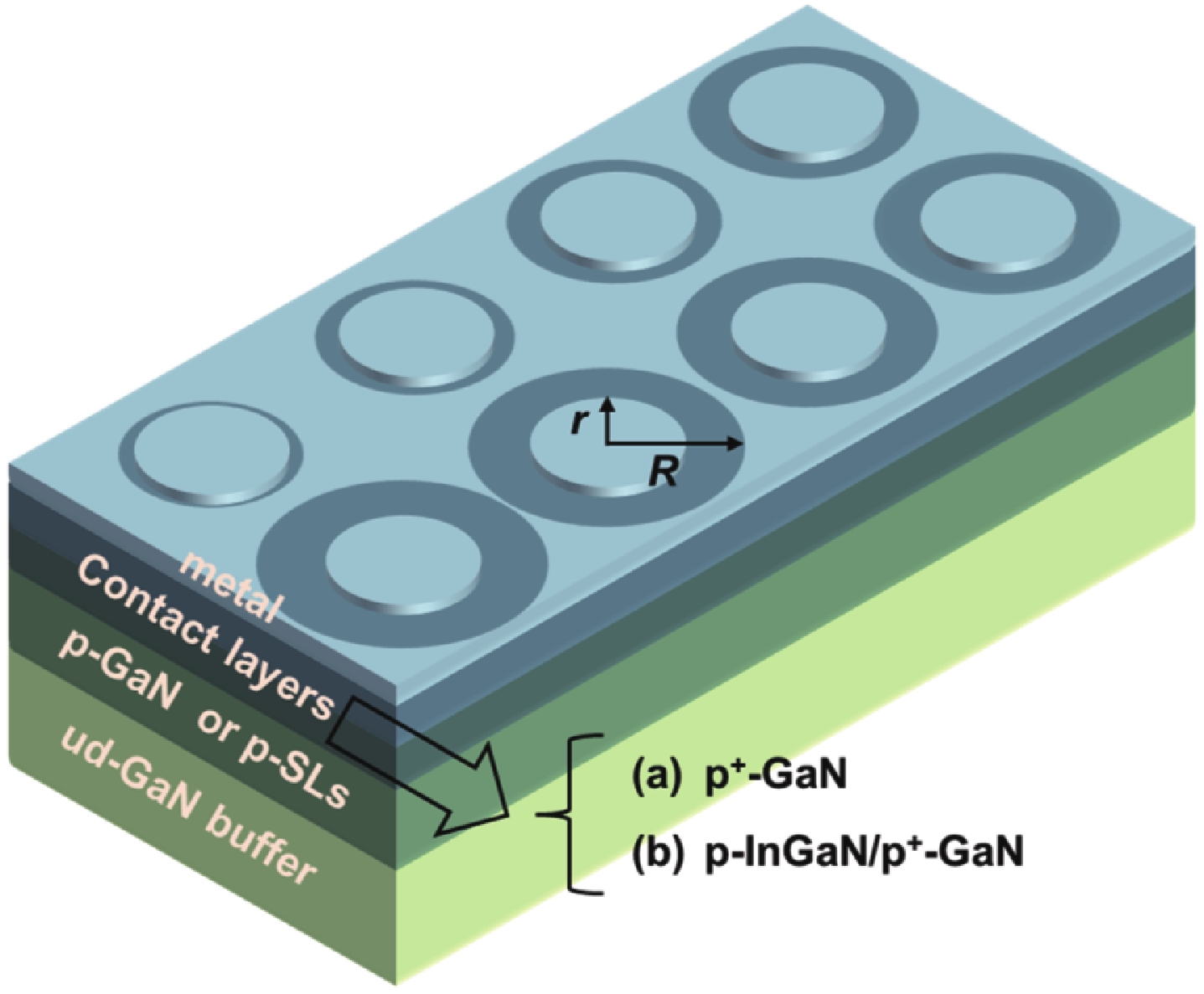
Fig. 1.
(Color online) Schematic illustration of the contact layer structure and c-TLM pattern used to measure contact resistance.
ARTICLES
Minglong Zhang1, 2, Masao Ikeda1, 2, , Siyi Huang1, 2, Jianping Liu1, 2, , Jianjun Zhu2, Shuming Zhang1, 2 and Hui Yang1, 2
Corresponding author: Masao Ikeda, mikeda2013@sinano.ac.cn; Jianping Liu, jpliu2010@sinano.ac.cn
Abstract: Specific contact resistance
Key words: GaN, ohmic contact, specific contact resistance
| [1] |
Nakamura S. The roles of structural imperfections in InGaN-based blue light-emitting diodes and laser diodes. Science, 1998, 281, 956 doi: 10.1126/science.281.5379.956
|
| [2] |
Hu L, Ren X Y, Liu J P, et al. High-power hybrid GaN-based green laser diodes with ITO cladding layer. Photonics Res, 2020, 8, 279 doi: 10.1364/PRJ.381262
|
| [3] |
Li L, Nomoto K, Pan M, et al. GaN HEMTs on Si with regrown contacts and cutoff/maximum oscillation frequencies of 250/204 GHz. IEEE Electron Device Lett, 2020, 41, 689 doi: 10.1109/LED.2020.2984727
|
| [4] |
Koide Y, Maeda T, Kawakami T, et al. Effects of annealing in an oxygen ambient on electrical properties of ohmic contacts to p-type GaN. J Electron Mater, 1999, 28, 341 doi: 10.1007/s11664-999-0037-7
|
| [5] |
Luther B P, Mohney S E, Jackson T N, et al. Investigation of the mechanism for Ohmic contact formation in Al and Ti/Al contacts to n-type GaN. Appl Phys Lett, 1997, 70, 57 doi: 10.1063/1.119305
|
| [6] |
Singh K, Chauhan A, Mathew M, et al. Formation of non-alloyed Ti/Al/Ni/Au low-resistance ohmic contacts on reactively ion-etched n-type GaN by surface treatment for GaN light-emitting diodes applications. Appl Phys A, 2019, 125, 24 doi: 10.1007/s00339-018-2322-x
|
| [7] |
Tanaka T, Watanabe A, Amano H, et al. P-type conduction in Mg-doped GaN and Al0.08Ga0.92N grown by metalorganic vapor phase epitaxy. Appl Phys Lett, 1994, 65, 593 doi: 10.1063/1.112309
|
| [8] |
Ho J K, Jong C S, Chiu C C, et al. Low-resistance ohmic contacts to p-type GaN. Appl Phys Lett, 1999, 74, 1275 doi: 10.1063/1.123546
|
| [9] |
Kim J K, Lee J L, Lee J W, et al. Low resistance Pd/Au ohmic contacts to p-type GaN using surface treatment. Appl Phys Lett, 1998, 73, 2953 doi: 10.1063/1.122641
|
| [10] |
Wahid S, Chowdhury N, Alam M K, et al. Barrier heights and Fermi level pinning in metal contacts on p-type GaN. Appl Phys Lett, 2020, 116, 213506 doi: 10.1063/5.0010699
|
| [11] |
Wang W J, Xie W Z, Deng Z J, et al. Performance improvement of GaN based laser diode using Pd/Ni/Au metallization ohmic contact. Coatings, 2019, 9, 291 doi: 10.3390/coatings9050291
|
| [12] |
Chary I, Chandolu A, Borisov B, et al. Influence of surface treatment and annealing temperature. J Electron Mater, 2009, 38, 545 doi: 10.1007/s11664-008-0655-5
|
| [13] |
Mallem S P R, Ahn W H, Lee J H, et al. Influence of thermal annealing on the PdAl/Au metal stack ohmic contacts to p-AlGaN. Crystals, 2020, 10, 1091 doi: 10.3390/cryst10121091
|
| [14] |
Lee J L, Weber M, Kim J K, et al. Ohmic contact formation mechanism of nonalloyed Pd contacts to p-type GaN observed by positron annihilation spectroscopy. Appl Phys Lett, 1999, 74, 2289 doi: 10.1063/1.123827
|
| [15] |
Song J O, Leem D S, Kwak J S, et al. High-quality nonalloyed rhodium-based ohmic contacts to p-type GaN. Appl Phys Lett, 2003, 83, 2372 doi: 10.1063/1.1613991
|
| [16] |
He J L, Zhong Y Z, Zhou Y, et al. Recovery of p-GaN surface damage induced by dry etching for the formation of p-type Ohmic contact. Appl Phys Express, 2019, 12, 055507 doi: 10.7567/1882-0786/ab13d7
|
| [17] |
Kumakura K, Makimoto T, Kobayashi N. Ohmic contact to p-GaN using a strained InGaN contact layer and its thermal stability. Jpn J Appl Phys, 2003, 42, 2254 doi: 10.1143/JJAP.42.2254
|
| [18] |
Trexler J T, Pearton S J, Holloway P H, et al. Comparison of Ni/Au, Pd/Au, and Cr/Au metallizations for ohmic contacts to p-GaN. MRS Online Proc Libr, 1996, 449, 1091 doi: 10.1557/PROC-449-1091
|
| [19] |
Bernardini F, Fiorentini V. Spontaneous versus piezoelectric polarization in III-V nitrides: Conceptual aspects and practical consequences. Phys Status Solidi B, 1999, 216, 391 doi: 10.1002/(SICI)1521-3951(199911)216:1<391::AID-PSSB391>3.0.CO;2-K
|
| [20] |
Weimar A, Lell A, Brüderl G, et al. Investigation of low-resistance metal contacts on p-type GaN using the linear and circular transmission line method. Phys Status Solidi A, 2001, 183, 169 doi: 10.1002/1521-396X(200101)183:1<169::AID-PSSA169>3.0.CO;2-D
|

Table 1. Details of the structures of Ni/Pd-based metals and p-InGaN/p+-GaN contacting layers.
| Sample | dp+-GaN (nm) | [Mg]p+-GaN (1020 cm–3) | dp-InGaN (nm) | [Mg]p-InGaN (1019 cm–3) | Xp-InGaN (%) | Metal scheme | Surface treatment |
| A | 25 | 1 | – | – | – | Ni 20 | w/o |
| B | 20 | 1 | 3.5 | 8 | 7 | Ni 20 | w/o |
| C | 22 | 1 | 2 | 4 | 20 | Ni/Pd 2/60 | w |
 DownLoad: CSV
| [1] |
Nakamura S. The roles of structural imperfections in InGaN-based blue light-emitting diodes and laser diodes. Science, 1998, 281, 956 doi: 10.1126/science.281.5379.956
|
| [2] |
Hu L, Ren X Y, Liu J P, et al. High-power hybrid GaN-based green laser diodes with ITO cladding layer. Photonics Res, 2020, 8, 279 doi: 10.1364/PRJ.381262
|
| [3] |
Li L, Nomoto K, Pan M, et al. GaN HEMTs on Si with regrown contacts and cutoff/maximum oscillation frequencies of 250/204 GHz. IEEE Electron Device Lett, 2020, 41, 689 doi: 10.1109/LED.2020.2984727
|
| [4] |
Koide Y, Maeda T, Kawakami T, et al. Effects of annealing in an oxygen ambient on electrical properties of ohmic contacts to p-type GaN. J Electron Mater, 1999, 28, 341 doi: 10.1007/s11664-999-0037-7
|
| [5] |
Luther B P, Mohney S E, Jackson T N, et al. Investigation of the mechanism for Ohmic contact formation in Al and Ti/Al contacts to n-type GaN. Appl Phys Lett, 1997, 70, 57 doi: 10.1063/1.119305
|
| [6] |
Singh K, Chauhan A, Mathew M, et al. Formation of non-alloyed Ti/Al/Ni/Au low-resistance ohmic contacts on reactively ion-etched n-type GaN by surface treatment for GaN light-emitting diodes applications. Appl Phys A, 2019, 125, 24 doi: 10.1007/s00339-018-2322-x
|
| [7] |
Tanaka T, Watanabe A, Amano H, et al. P-type conduction in Mg-doped GaN and Al0.08Ga0.92N grown by metalorganic vapor phase epitaxy. Appl Phys Lett, 1994, 65, 593 doi: 10.1063/1.112309
|
| [8] |
Ho J K, Jong C S, Chiu C C, et al. Low-resistance ohmic contacts to p-type GaN. Appl Phys Lett, 1999, 74, 1275 doi: 10.1063/1.123546
|
| [9] |
Kim J K, Lee J L, Lee J W, et al. Low resistance Pd/Au ohmic contacts to p-type GaN using surface treatment. Appl Phys Lett, 1998, 73, 2953 doi: 10.1063/1.122641
|
| [10] |
Wahid S, Chowdhury N, Alam M K, et al. Barrier heights and Fermi level pinning in metal contacts on p-type GaN. Appl Phys Lett, 2020, 116, 213506 doi: 10.1063/5.0010699
|
| [11] |
Wang W J, Xie W Z, Deng Z J, et al. Performance improvement of GaN based laser diode using Pd/Ni/Au metallization ohmic contact. Coatings, 2019, 9, 291 doi: 10.3390/coatings9050291
|
| [12] |
Chary I, Chandolu A, Borisov B, et al. Influence of surface treatment and annealing temperature. J Electron Mater, 2009, 38, 545 doi: 10.1007/s11664-008-0655-5
|
| [13] |
Mallem S P R, Ahn W H, Lee J H, et al. Influence of thermal annealing on the PdAl/Au metal stack ohmic contacts to p-AlGaN. Crystals, 2020, 10, 1091 doi: 10.3390/cryst10121091
|
| [14] |
Lee J L, Weber M, Kim J K, et al. Ohmic contact formation mechanism of nonalloyed Pd contacts to p-type GaN observed by positron annihilation spectroscopy. Appl Phys Lett, 1999, 74, 2289 doi: 10.1063/1.123827
|
| [15] |
Song J O, Leem D S, Kwak J S, et al. High-quality nonalloyed rhodium-based ohmic contacts to p-type GaN. Appl Phys Lett, 2003, 83, 2372 doi: 10.1063/1.1613991
|
| [16] |
He J L, Zhong Y Z, Zhou Y, et al. Recovery of p-GaN surface damage induced by dry etching for the formation of p-type Ohmic contact. Appl Phys Express, 2019, 12, 055507 doi: 10.7567/1882-0786/ab13d7
|
| [17] |
Kumakura K, Makimoto T, Kobayashi N. Ohmic contact to p-GaN using a strained InGaN contact layer and its thermal stability. Jpn J Appl Phys, 2003, 42, 2254 doi: 10.1143/JJAP.42.2254
|
| [18] |
Trexler J T, Pearton S J, Holloway P H, et al. Comparison of Ni/Au, Pd/Au, and Cr/Au metallizations for ohmic contacts to p-GaN. MRS Online Proc Libr, 1996, 449, 1091 doi: 10.1557/PROC-449-1091
|
| [19] |
Bernardini F, Fiorentini V. Spontaneous versus piezoelectric polarization in III-V nitrides: Conceptual aspects and practical consequences. Phys Status Solidi B, 1999, 216, 391 doi: 10.1002/(SICI)1521-3951(199911)216:1<391::AID-PSSB391>3.0.CO;2-K
|
| [20] |
Weimar A, Lell A, Brüderl G, et al. Investigation of low-resistance metal contacts on p-type GaN using the linear and circular transmission line method. Phys Status Solidi A, 2001, 183, 169 doi: 10.1002/1521-396X(200101)183:1<169::AID-PSSA169>3.0.CO;2-D
|


Article views: 2355 Times PDF downloads: 233 Times Cited by: 0 Times
Received: 29 March 2022 Revised: 08 May 2022 Online: Accepted Manuscript: 26 June 2022Uncorrected proof: 27 June 2022Published: 02 September 2022
| Citation: |
Minglong Zhang, Masao Ikeda, Siyi Huang, Jianping Liu, Jianjun Zhu, Shuming Zhang, Hui Yang. Ni/Pd-based ohmic contacts to p-GaN through p-InGaN/p+-GaN contacting layers[J]. Journal of Semiconductors, 2022, 43(9): 092803. doi: 10.1088/1674-4926/43/9/092803
****
M L Zhang, M Ikeda, S Y Huang, J P Liu, J J Zhu, S M Zhang, H Yang. Ni/Pd-based ohmic contacts to p-GaN through p-InGaN/p+-GaN contacting layers[J]. J. Semicond, 2022, 43(9): 092803. doi: 10.1088/1674-4926/43/9/092803

|
| [1] |
Nakamura S. The roles of structural imperfections in InGaN-based blue light-emitting diodes and laser diodes. Science, 1998, 281, 956 doi: 10.1126/science.281.5379.956
|
| [2] |
Hu L, Ren X Y, Liu J P, et al. High-power hybrid GaN-based green laser diodes with ITO cladding layer. Photonics Res, 2020, 8, 279 doi: 10.1364/PRJ.381262
|
| [3] |
Li L, Nomoto K, Pan M, et al. GaN HEMTs on Si with regrown contacts and cutoff/maximum oscillation frequencies of 250/204 GHz. IEEE Electron Device Lett, 2020, 41, 689 doi: 10.1109/LED.2020.2984727
|
| [4] |
Koide Y, Maeda T, Kawakami T, et al. Effects of annealing in an oxygen ambient on electrical properties of ohmic contacts to p-type GaN. J Electron Mater, 1999, 28, 341 doi: 10.1007/s11664-999-0037-7
|
| [5] |
Luther B P, Mohney S E, Jackson T N, et al. Investigation of the mechanism for Ohmic contact formation in Al and Ti/Al contacts to n-type GaN. Appl Phys Lett, 1997, 70, 57 doi: 10.1063/1.119305
|
| [6] |
Singh K, Chauhan A, Mathew M, et al. Formation of non-alloyed Ti/Al/Ni/Au low-resistance ohmic contacts on reactively ion-etched n-type GaN by surface treatment for GaN light-emitting diodes applications. Appl Phys A, 2019, 125, 24 doi: 10.1007/s00339-018-2322-x
|
| [7] |
Tanaka T, Watanabe A, Amano H, et al. P-type conduction in Mg-doped GaN and Al0.08Ga0.92N grown by metalorganic vapor phase epitaxy. Appl Phys Lett, 1994, 65, 593 doi: 10.1063/1.112309
|
| [8] |
Ho J K, Jong C S, Chiu C C, et al. Low-resistance ohmic contacts to p-type GaN. Appl Phys Lett, 1999, 74, 1275 doi: 10.1063/1.123546
|
| [9] |
Kim J K, Lee J L, Lee J W, et al. Low resistance Pd/Au ohmic contacts to p-type GaN using surface treatment. Appl Phys Lett, 1998, 73, 2953 doi: 10.1063/1.122641
|
| [10] |
Wahid S, Chowdhury N, Alam M K, et al. Barrier heights and Fermi level pinning in metal contacts on p-type GaN. Appl Phys Lett, 2020, 116, 213506 doi: 10.1063/5.0010699
|
| [11] |
Wang W J, Xie W Z, Deng Z J, et al. Performance improvement of GaN based laser diode using Pd/Ni/Au metallization ohmic contact. Coatings, 2019, 9, 291 doi: 10.3390/coatings9050291
|
| [12] |
Chary I, Chandolu A, Borisov B, et al. Influence of surface treatment and annealing temperature. J Electron Mater, 2009, 38, 545 doi: 10.1007/s11664-008-0655-5
|
| [13] |
Mallem S P R, Ahn W H, Lee J H, et al. Influence of thermal annealing on the PdAl/Au metal stack ohmic contacts to p-AlGaN. Crystals, 2020, 10, 1091 doi: 10.3390/cryst10121091
|
| [14] |
Lee J L, Weber M, Kim J K, et al. Ohmic contact formation mechanism of nonalloyed Pd contacts to p-type GaN observed by positron annihilation spectroscopy. Appl Phys Lett, 1999, 74, 2289 doi: 10.1063/1.123827
|
| [15] |
Song J O, Leem D S, Kwak J S, et al. High-quality nonalloyed rhodium-based ohmic contacts to p-type GaN. Appl Phys Lett, 2003, 83, 2372 doi: 10.1063/1.1613991
|
| [16] |
He J L, Zhong Y Z, Zhou Y, et al. Recovery of p-GaN surface damage induced by dry etching for the formation of p-type Ohmic contact. Appl Phys Express, 2019, 12, 055507 doi: 10.7567/1882-0786/ab13d7
|
| [17] |
Kumakura K, Makimoto T, Kobayashi N. Ohmic contact to p-GaN using a strained InGaN contact layer and its thermal stability. Jpn J Appl Phys, 2003, 42, 2254 doi: 10.1143/JJAP.42.2254
|
| [18] |
Trexler J T, Pearton S J, Holloway P H, et al. Comparison of Ni/Au, Pd/Au, and Cr/Au metallizations for ohmic contacts to p-GaN. MRS Online Proc Libr, 1996, 449, 1091 doi: 10.1557/PROC-449-1091
|
| [19] |
Bernardini F, Fiorentini V. Spontaneous versus piezoelectric polarization in III-V nitrides: Conceptual aspects and practical consequences. Phys Status Solidi B, 1999, 216, 391 doi: 10.1002/(SICI)1521-3951(199911)216:1<391::AID-PSSB391>3.0.CO;2-K
|
| [20] |
Weimar A, Lell A, Brüderl G, et al. Investigation of low-resistance metal contacts on p-type GaN using the linear and circular transmission line method. Phys Status Solidi A, 2001, 183, 169 doi: 10.1002/1521-396X(200101)183:1<169::AID-PSSA169>3.0.CO;2-D
|

 WeChat ID
Journal of Semiconductors © 2017 All Rights Reserved 京ICP備05085259號-2


