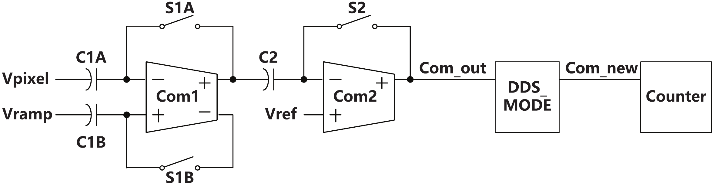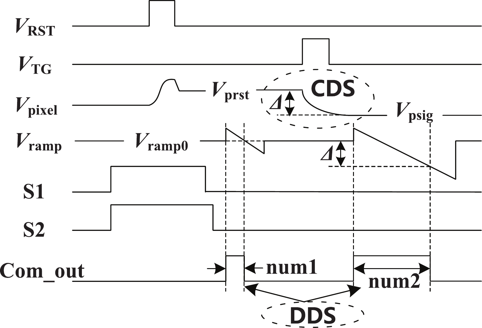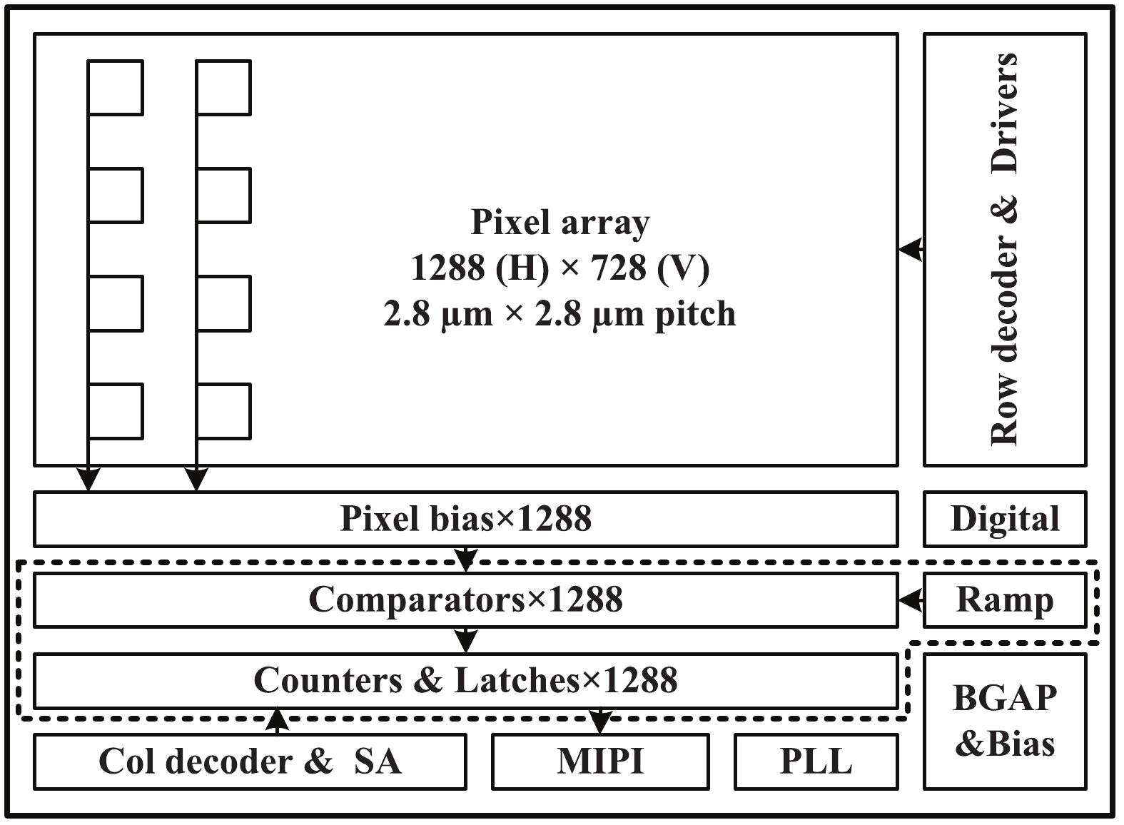
Fig. 1.
Block diagram of the overall architecture.
ARTICLES
Wenjing Xu1, 2, Jie Chen1, , Zhangqu Kuang3, Li Zhou1, Ming Chen1 and Chengbin Zhang1
Corresponding author: Jie Chen, jchen@ime.ac.cn
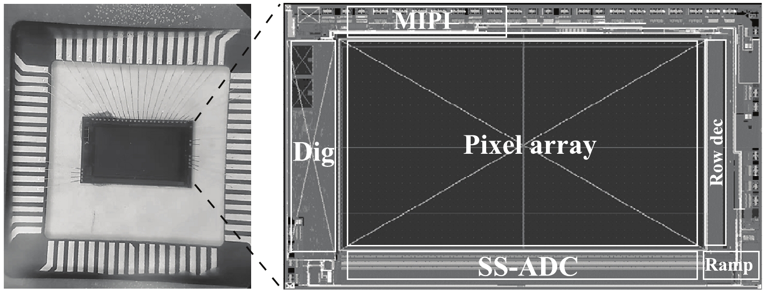
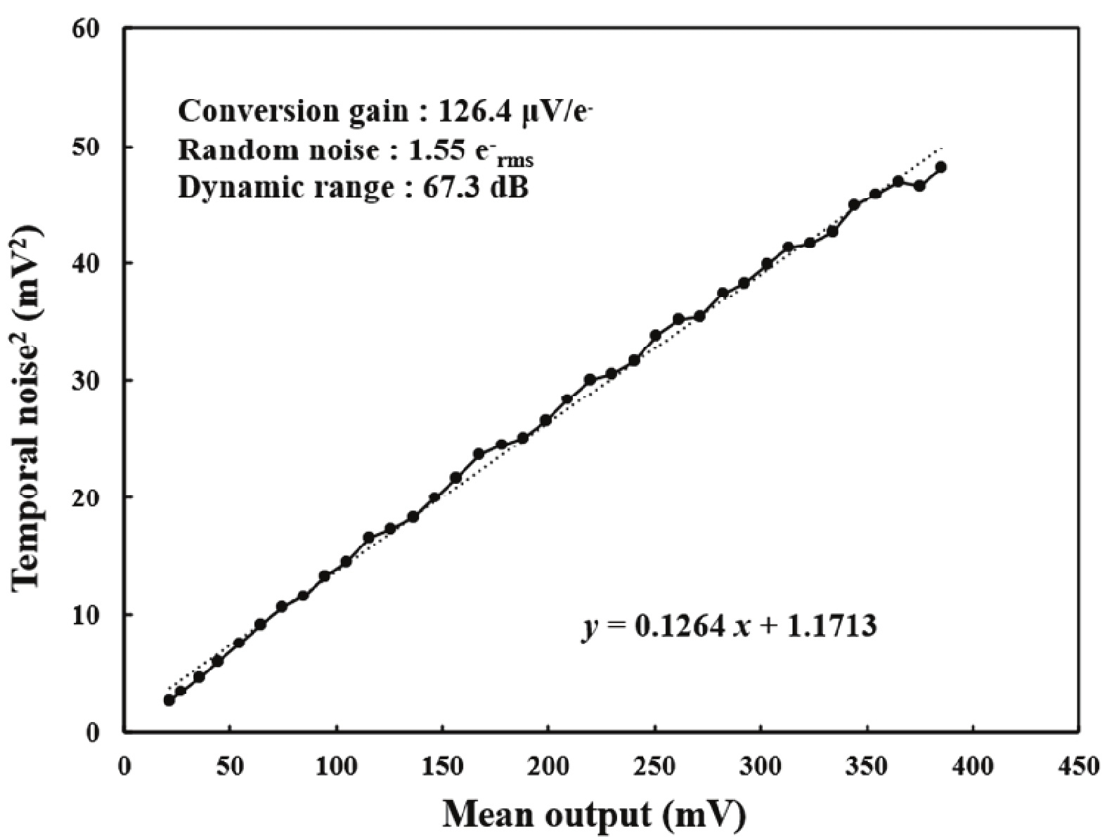
Abstract: This paper presents a low-power high-quality CMOS image sensor (CIS) using 1.5 V 4T pinned photodiode (4T-PPD) and dual correlated double sampling (dual-CDS) column-parallel single-slope ADC. A five-finger shaped pixel layer is proposed to solve image lag caused by low-voltage 4T-PPD. Dual-CDS is used to reduce random noise and the nonuniformity between columns. Dual-mode counting method is proposed to improve circuit robustness. A prototype sensor was fabricated using a 0.11 μm CMOS process. Measurement results show that the lag of the five-finger shaped pixel is reduced by 80% compared with the conventional rectangular pixel, the chip power consumption is only 36 mW, the dynamic range is 67.3 dB, the random noise is only 1.55 e–rms, and the figure-of-merit is only 1.98 e–·nJ, thus realizing low-power and high-quality imaging.
Key words: CMOS image sensor, 4T pinned photodiode, single-slope ADC, correlated double sample, counting method
| [1] |
Park I, Jo W, Park C, et al. A 640 × 640 fully dynamic CMOS image sensor for always-on operation. IEEE J Solid State Circuits, 2020, 55, 898 doi: 10.1109/JSSC.2019.2959486
|
| [2] |
Hsu T H, Chen Y R, Liu R S, et al. A 0.5-V real-time computational CMOS image sensor with programmable kernel for feature extraction. IEEE J Solid State Circuits, 2021, 56, 1588 doi: 10.1109/JSSC.2020.3034192
|
| [3] |
Hanson S, Foo Z, Blaauw D, et al. A 0.5 V sub-microwatt CMOS image sensor with pulse-width modulation read-out. IEEE J Solid State Circuits, 2010, 45, 759 doi: 10.1109/JSSC.2010.2040231
|
| [4] |
Couniot N, de Streel G, Botman F, et al. A 65 nm 0.5 V DPS CMOS image sensor with 17 pJ/Frame. Pixel and 42 dB dynamic range for ultra-low-power SoCs. IEEE J Solid State Circuits, 2015, 50, 2419 doi: 10.1109/JSSC.2015.2457897
|
| [5] |
Cho K B, Krymski A I, Fossum E R. A 1.5-V 550-μW 176 × 144 autonomous CMOS active pixel image sensor. IEEE Trans Electron Devices, 2003, 50, 96 doi: 10.1109/TED.2002.806475
|
| [6] |
Choi J, Shin J, Kang D W, et al. Always-on CMOS image sensor for mobile and wearable devices. IEEE J Solid State Circuits, 2016, 51, 130 doi: 10.1109/JSSC.2015.2470526
|
| [7] |
Nitta Y, Muramatsu Y, Amano K, et al. High-speed digital double sampling with analog CDS on column parallel ADC architecture for low-noise active pixel sensor. 2006 IEEE International Solid State Circuits Conference, 2006, 2024
|
| [8] |
Liu Q Y, Edward A, Kinyua M, et al. A low-power digitizer for back-illuminated 3-D-stacked CMOS image sensor readout with passing window and double auto-zeroing techniques. IEEE J Solid State Circuits, 2017, 52, 1591 doi: 10.1109/JSSC.2017.2661843
|
| [9] |
Park I, Park C, Cheon J, et al. A 76mW 500fps VGA CMOS image sensor with time-stretched single-slope ADCs achieving 1.95e- random noise. 2019 IEEE International Solid-State Circuits Conference, 2019, 100
|
| [10] |
Kim H J. 11-bit column-parallel single-slope ADC with first-step half-reference ramping scheme for high-speed CMOS image sensors. IEEE J Solid State Circuits, 2021, 56, 2132 doi: 10.1109/JSSC.2021.3059909
|
| [11] |
Shin B, Park S, Shin H. The effect of photodiode shape on charge transfer in CMOS image sensors. Solid State Electron, 2010, 54, 1416 doi: 10.1016/j.sse.2010.06.006
|
| [12] |
Xu Y, Theuwissen A J. Image lag analysis and photodiode shape optimization of 4T CMOS pixels. International Image Sensor Workshop, 2013
|
| [13] |
Cao X Z, Gäbler D, Lee C, et al. Design and optimization of large 4T pixel. International Image Sensor Workshop, 2015
|
| [14] |
Acerbi F, Garcia M M, Köklü G, et al. Transfer-gate region optimization and pinned-photodiode shaping for high-speed ToF applications. International Image Sensor Workshop, 2017
|
| [15] |
Millar T C, Sarhangnejad N, Katic N, et al. The effect of pinned photodiode shape on time-of-flight demodulation contrast. IEEE Trans Electron Devices, 2017, 64, 2244 doi: 10.1109/TED.2017.2677201
|
| [16] |
Kawahito S. Column-parallel ADCs for CMOS image sensors and their FoM-based evaluations. IEICE Trans Electron, 2018, E101.C, 444 doi: 10.1587/transele.E101.C.444
|
| [17] |
Nie K M, Zha W B, Shi X L, et al. A single slope ADC with row-wise noise reduction technique for CMOS image sensor. IEEE Trans Circuits Syst I, 2020, 67, 2873 doi: 10.1109/TCSI.2020.2979321
|
| [18] |
Park H, Yu C Z, Kim H, et al. Low power CMOS image sensors using two step single slope ADC with bandwidth-limited comparators & voltage range extended ramp generator for battery-limited application. IEEE Sens J, 2020, 20, 2831 doi: 10.1109/JSEN.2019.2957043
|
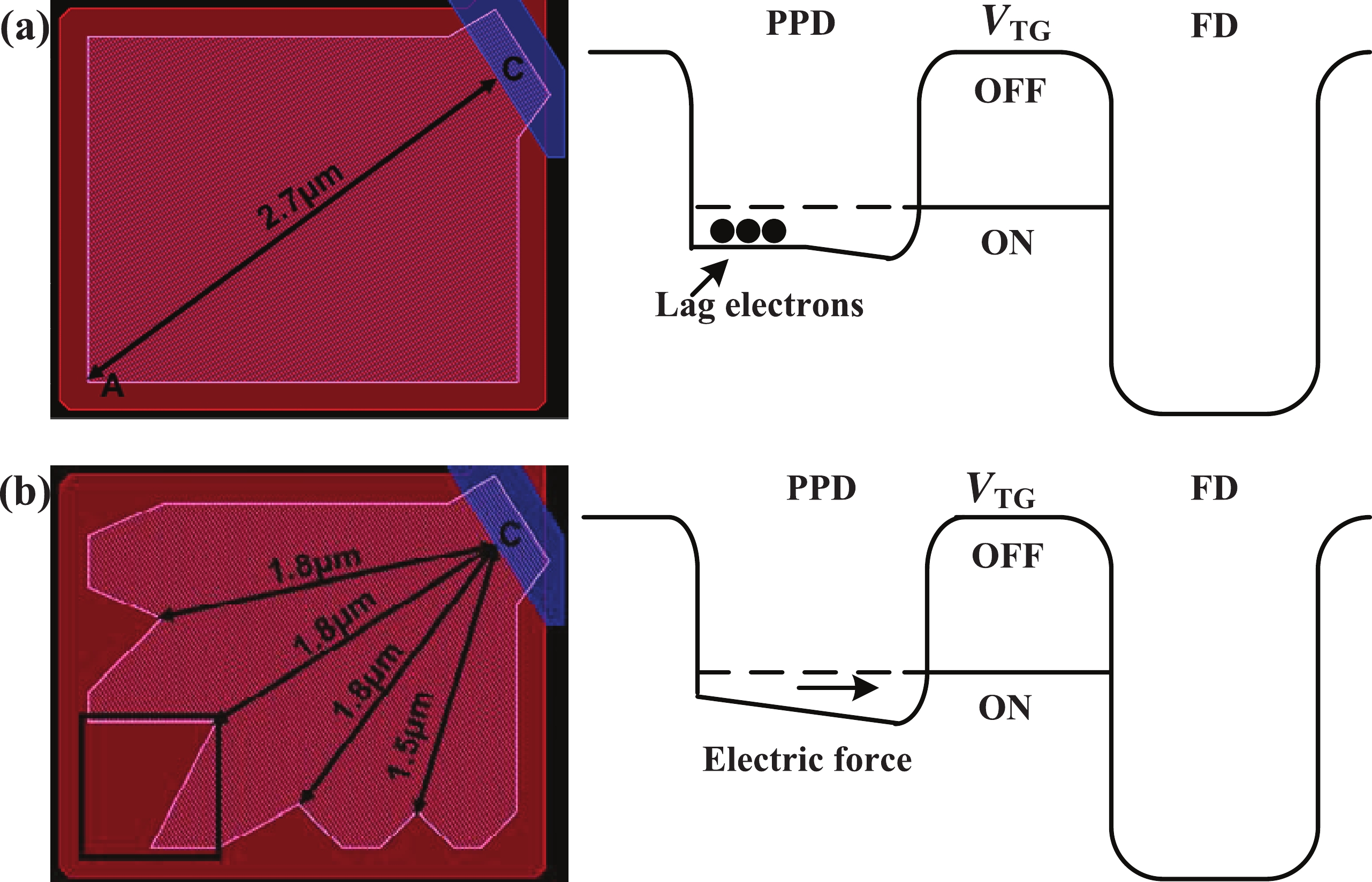

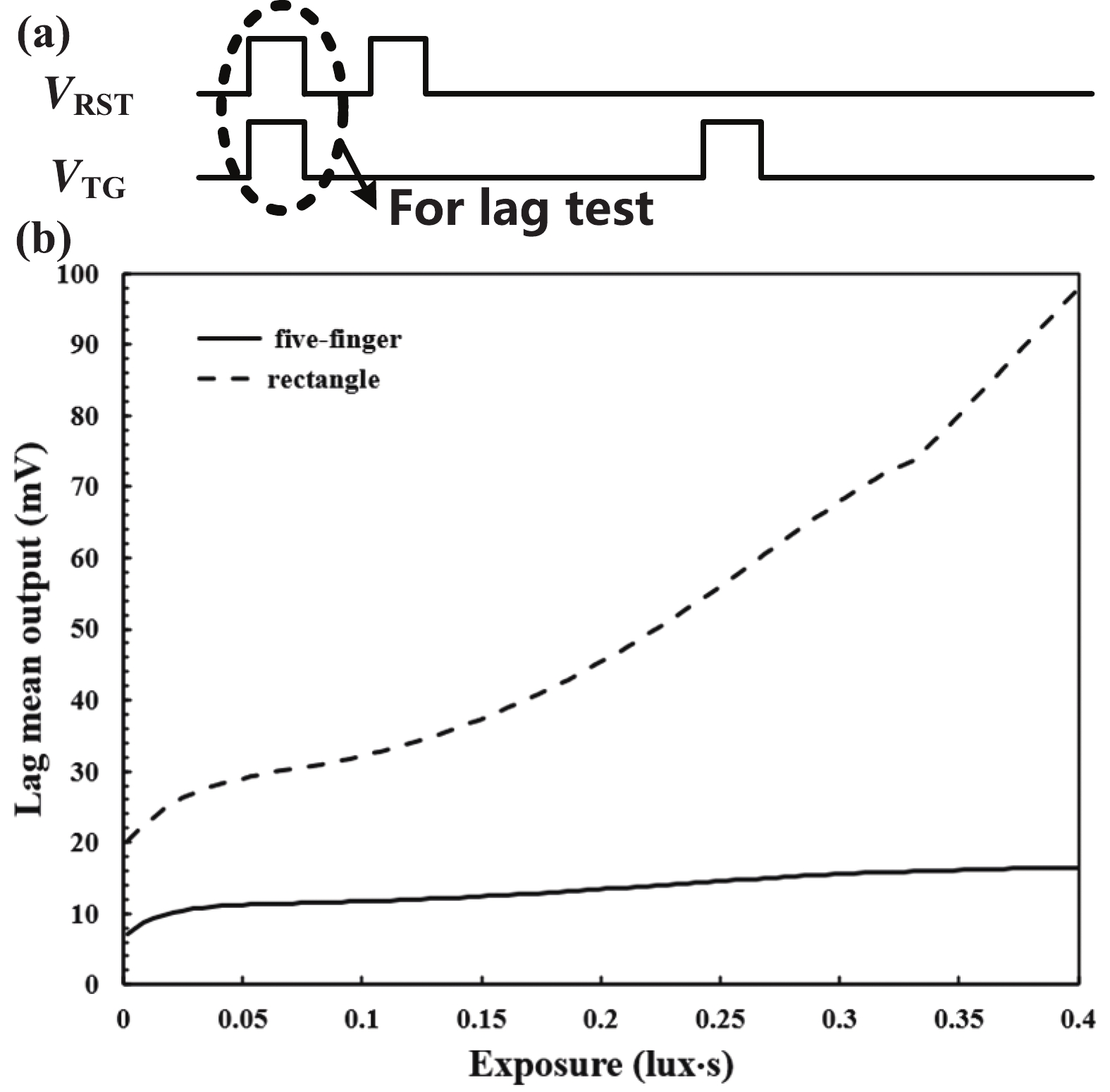
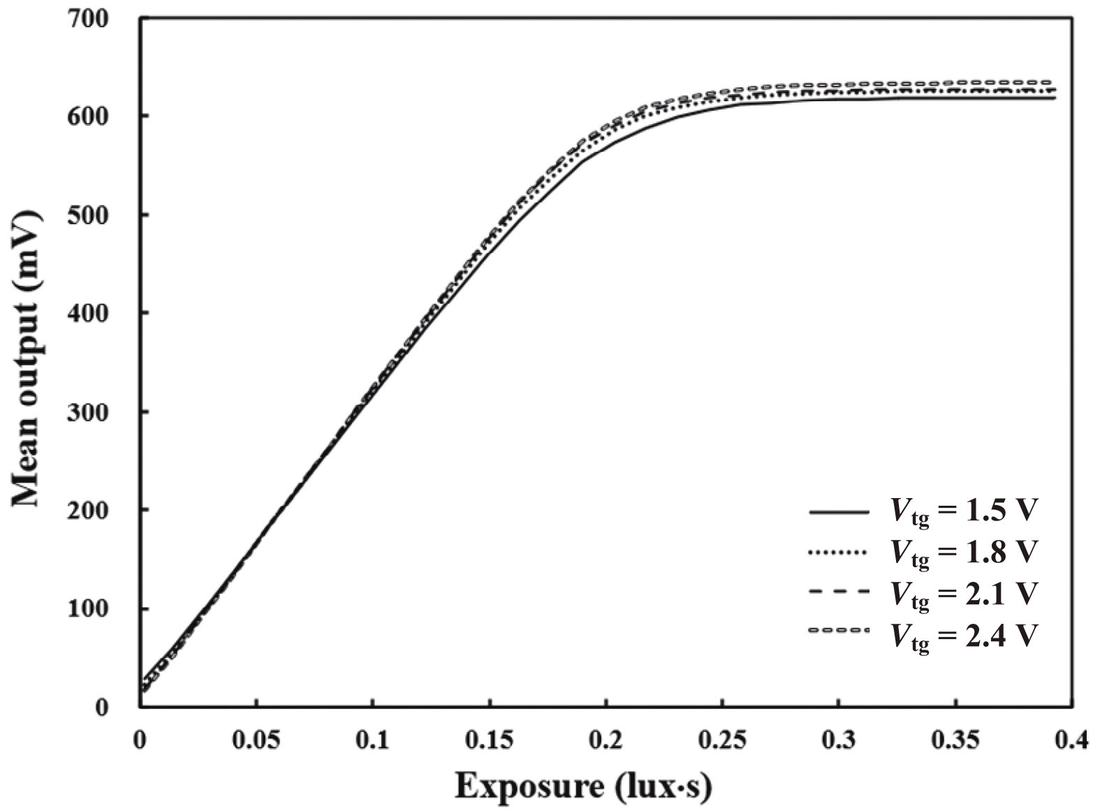

Table 1. Chip power consumption.
| Parameter | Voltage (V) | Current (A) | Power consumption (mW) |
| Pixel and analog | 1.5 | 10.35 | 15.525 |
| Digital | 1.2 | 16.96 | 20.352 |
| I/O | 1.8 | 0.03 | 0.054 |
| Sum | 35.931 |
 DownLoad: CSV
Table 2. Comparison with other published CIS.
| Parameter | This work | JSSC[6] | TCASI[17] | Sensor[18] | JSSC[4] | |
| Process (nm) | 110 | 110 | 110 | 90 | 65 | |
| Pixel pitch (μm) | 2.8 | 5.0 | 6.5 | 5.6 | 4.0 | |
| Pixel type | 4T PPD | 4T PPD | 4T PPD | 4T PPD | Digital | |
| Pixel resolution | 1288 × 728 | 640 × 480 | 320 × 240 | 128 × 128 | 960 × 720 | 128 × 128 |
| Frame rate (fps) | 30 | 15 | 15 | 228 | 35 | 32 |
| Power supply (V) | 1.5/1.2 | 3.3/1.8 | 0.9 | 3.3/1.5 | 2.8/1.5 | 0.5 |
| Dynamic range (dB) | 67.3 | 69 | 50 | 68.9 | 66.7 | 42 |
| Power consumption (mW) | 36 | 2.28 | 0.0455 | 40 | 28 | 0.0088 |
| Random noise (e–rms) | 1.55 | 5.5 | 83.7 | 3.25* | 3.73* | 416 |
| FoM (e–·nJ) | 1.98 | 2.72 | 3.31 | 34.8 | 4.32 | 6.98 |
| * For fair comparison, conversion gain is assumed by 126.4 μV/e–. | ||||||
DownLoad: CSV
| [1] |
Park I, Jo W, Park C, et al. A 640 × 640 fully dynamic CMOS image sensor for always-on operation. IEEE J Solid State Circuits, 2020, 55, 898 doi: 10.1109/JSSC.2019.2959486
|
| [2] |
Hsu T H, Chen Y R, Liu R S, et al. A 0.5-V real-time computational CMOS image sensor with programmable kernel for feature extraction. IEEE J Solid State Circuits, 2021, 56, 1588 doi: 10.1109/JSSC.2020.3034192
|
| [3] |
Hanson S, Foo Z, Blaauw D, et al. A 0.5 V sub-microwatt CMOS image sensor with pulse-width modulation read-out. IEEE J Solid State Circuits, 2010, 45, 759 doi: 10.1109/JSSC.2010.2040231
|
| [4] |
Couniot N, de Streel G, Botman F, et al. A 65 nm 0.5 V DPS CMOS image sensor with 17 pJ/Frame. Pixel and 42 dB dynamic range for ultra-low-power SoCs. IEEE J Solid State Circuits, 2015, 50, 2419 doi: 10.1109/JSSC.2015.2457897
|
| [5] |
Cho K B, Krymski A I, Fossum E R. A 1.5-V 550-μW 176 × 144 autonomous CMOS active pixel image sensor. IEEE Trans Electron Devices, 2003, 50, 96 doi: 10.1109/TED.2002.806475
|
| [6] |
Choi J, Shin J, Kang D W, et al. Always-on CMOS image sensor for mobile and wearable devices. IEEE J Solid State Circuits, 2016, 51, 130 doi: 10.1109/JSSC.2015.2470526
|
| [7] |
Nitta Y, Muramatsu Y, Amano K, et al. High-speed digital double sampling with analog CDS on column parallel ADC architecture for low-noise active pixel sensor. 2006 IEEE International Solid State Circuits Conference, 2006, 2024
|
| [8] |
Liu Q Y, Edward A, Kinyua M, et al. A low-power digitizer for back-illuminated 3-D-stacked CMOS image sensor readout with passing window and double auto-zeroing techniques. IEEE J Solid State Circuits, 2017, 52, 1591 doi: 10.1109/JSSC.2017.2661843
|
| [9] |
Park I, Park C, Cheon J, et al. A 76mW 500fps VGA CMOS image sensor with time-stretched single-slope ADCs achieving 1.95e- random noise. 2019 IEEE International Solid-State Circuits Conference, 2019, 100
|
| [10] |
Kim H J. 11-bit column-parallel single-slope ADC with first-step half-reference ramping scheme for high-speed CMOS image sensors. IEEE J Solid State Circuits, 2021, 56, 2132 doi: 10.1109/JSSC.2021.3059909
|
| [11] |
Shin B, Park S, Shin H. The effect of photodiode shape on charge transfer in CMOS image sensors. Solid State Electron, 2010, 54, 1416 doi: 10.1016/j.sse.2010.06.006
|
| [12] |
Xu Y, Theuwissen A J. Image lag analysis and photodiode shape optimization of 4T CMOS pixels. International Image Sensor Workshop, 2013
|
| [13] |
Cao X Z, Gäbler D, Lee C, et al. Design and optimization of large 4T pixel. International Image Sensor Workshop, 2015
|
| [14] |
Acerbi F, Garcia M M, Köklü G, et al. Transfer-gate region optimization and pinned-photodiode shaping for high-speed ToF applications. International Image Sensor Workshop, 2017
|
| [15] |
Millar T C, Sarhangnejad N, Katic N, et al. The effect of pinned photodiode shape on time-of-flight demodulation contrast. IEEE Trans Electron Devices, 2017, 64, 2244 doi: 10.1109/TED.2017.2677201
|
| [16] |
Kawahito S. Column-parallel ADCs for CMOS image sensors and their FoM-based evaluations. IEICE Trans Electron, 2018, E101.C, 444 doi: 10.1587/transele.E101.C.444
|
| [17] |
Nie K M, Zha W B, Shi X L, et al. A single slope ADC with row-wise noise reduction technique for CMOS image sensor. IEEE Trans Circuits Syst I, 2020, 67, 2873 doi: 10.1109/TCSI.2020.2979321
|
| [18] |
Park H, Yu C Z, Kim H, et al. Low power CMOS image sensors using two step single slope ADC with bandwidth-limited comparators & voltage range extended ramp generator for battery-limited application. IEEE Sens J, 2020, 20, 2831 doi: 10.1109/JSEN.2019.2957043
|


Article views: 4673 Times PDF downloads: 266 Times Cited by: 0 Times
Received: 09 November 2021 Revised: 16 February 2022 Online: Accepted Manuscript: 13 May 2022Uncorrected proof: 19 May 2022Published: 01 August 2022
| Citation: |
Wenjing Xu, Jie Chen, Zhangqu Kuang, Li Zhou, Ming Chen, Chengbin Zhang. A low-power high-quality CMOS image sensor using 1.5 V 4T pinned photodiode and dual-CDS column-parallel single-slope ADC[J]. Journal of Semiconductors, 2022, 43(8): 082401. doi: 10.1088/1674-4926/43/8/082401
****
W J Xu, J Chen, Z Q Kuang, L Zhou, M Chen, C B Zhang. A low-power high-quality CMOS image sensor using 1.5 V 4T pinned photodiode and dual-CDS column-parallel single-slope ADC[J]. J. Semicond, 2022, 43(8): 082401. doi: 10.1088/1674-4926/43/8/082401

|
| [1] |
Park I, Jo W, Park C, et al. A 640 × 640 fully dynamic CMOS image sensor for always-on operation. IEEE J Solid State Circuits, 2020, 55, 898 doi: 10.1109/JSSC.2019.2959486
|
| [2] |
Hsu T H, Chen Y R, Liu R S, et al. A 0.5-V real-time computational CMOS image sensor with programmable kernel for feature extraction. IEEE J Solid State Circuits, 2021, 56, 1588 doi: 10.1109/JSSC.2020.3034192
|
| [3] |
Hanson S, Foo Z, Blaauw D, et al. A 0.5 V sub-microwatt CMOS image sensor with pulse-width modulation read-out. IEEE J Solid State Circuits, 2010, 45, 759 doi: 10.1109/JSSC.2010.2040231
|
| [4] |
Couniot N, de Streel G, Botman F, et al. A 65 nm 0.5 V DPS CMOS image sensor with 17 pJ/Frame. Pixel and 42 dB dynamic range for ultra-low-power SoCs. IEEE J Solid State Circuits, 2015, 50, 2419 doi: 10.1109/JSSC.2015.2457897
|
| [5] |
Cho K B, Krymski A I, Fossum E R. A 1.5-V 550-μW 176 × 144 autonomous CMOS active pixel image sensor. IEEE Trans Electron Devices, 2003, 50, 96 doi: 10.1109/TED.2002.806475
|
| [6] |
Choi J, Shin J, Kang D W, et al. Always-on CMOS image sensor for mobile and wearable devices. IEEE J Solid State Circuits, 2016, 51, 130 doi: 10.1109/JSSC.2015.2470526
|
| [7] |
Nitta Y, Muramatsu Y, Amano K, et al. High-speed digital double sampling with analog CDS on column parallel ADC architecture for low-noise active pixel sensor. 2006 IEEE International Solid State Circuits Conference, 2006, 2024
|
| [8] |
Liu Q Y, Edward A, Kinyua M, et al. A low-power digitizer for back-illuminated 3-D-stacked CMOS image sensor readout with passing window and double auto-zeroing techniques. IEEE J Solid State Circuits, 2017, 52, 1591 doi: 10.1109/JSSC.2017.2661843
|
| [9] |
Park I, Park C, Cheon J, et al. A 76mW 500fps VGA CMOS image sensor with time-stretched single-slope ADCs achieving 1.95e- random noise. 2019 IEEE International Solid-State Circuits Conference, 2019, 100
|
| [10] |
Kim H J. 11-bit column-parallel single-slope ADC with first-step half-reference ramping scheme for high-speed CMOS image sensors. IEEE J Solid State Circuits, 2021, 56, 2132 doi: 10.1109/JSSC.2021.3059909
|
| [11] |
Shin B, Park S, Shin H. The effect of photodiode shape on charge transfer in CMOS image sensors. Solid State Electron, 2010, 54, 1416 doi: 10.1016/j.sse.2010.06.006
|
| [12] |
Xu Y, Theuwissen A J. Image lag analysis and photodiode shape optimization of 4T CMOS pixels. International Image Sensor Workshop, 2013
|
| [13] |
Cao X Z, Gäbler D, Lee C, et al. Design and optimization of large 4T pixel. International Image Sensor Workshop, 2015
|
| [14] |
Acerbi F, Garcia M M, Köklü G, et al. Transfer-gate region optimization and pinned-photodiode shaping for high-speed ToF applications. International Image Sensor Workshop, 2017
|
| [15] |
Millar T C, Sarhangnejad N, Katic N, et al. The effect of pinned photodiode shape on time-of-flight demodulation contrast. IEEE Trans Electron Devices, 2017, 64, 2244 doi: 10.1109/TED.2017.2677201
|
| [16] |
Kawahito S. Column-parallel ADCs for CMOS image sensors and their FoM-based evaluations. IEICE Trans Electron, 2018, E101.C, 444 doi: 10.1587/transele.E101.C.444
|
| [17] |
Nie K M, Zha W B, Shi X L, et al. A single slope ADC with row-wise noise reduction technique for CMOS image sensor. IEEE Trans Circuits Syst I, 2020, 67, 2873 doi: 10.1109/TCSI.2020.2979321
|
| [18] |
Park H, Yu C Z, Kim H, et al. Low power CMOS image sensors using two step single slope ADC with bandwidth-limited comparators & voltage range extended ramp generator for battery-limited application. IEEE Sens J, 2020, 20, 2831 doi: 10.1109/JSEN.2019.2957043
|

 WeChat ID
Journal of Semiconductors © 2017 All Rights Reserved 京ICP備05085259號-2