


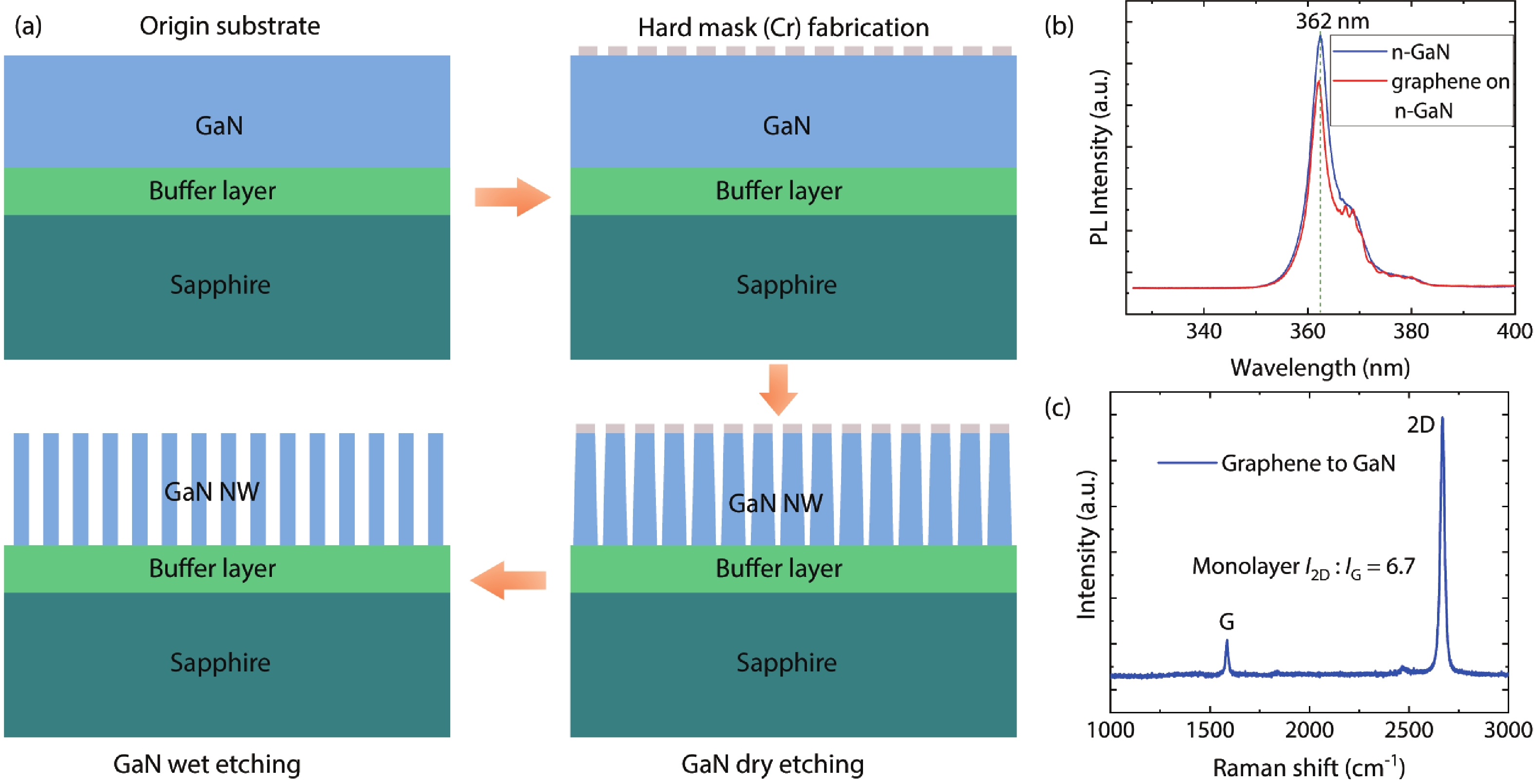
Fig. 1.
(Color online) (a) The process schematic diagram of the preparation of GaN nanorods. (b) The PL spectra of GaN before and after graphene transfer. (c) The Raman spectra of graphene grown on copper foil.
ARTICLES
Xuemin Zhang1, 2, Changling Yan1, , Jinghang Yang1, Chao Pang1, Yunzhen Yue1, Chunhong Zeng1, 2 and Baoshun Zhang2,
Corresponding author: Changling Yan, changling_yan@126.com; Baoshun Zhang, bszhang2006@sinano.ac.cn
Abstract: GaN has been widely used in the fabrication of ultraviolet photodetectors because of its outstanding properties. In this paper, we report a graphene–GaN nanorod heterostructure photodetector with fast photoresponse in the UV range. GaN nanorods were fabricated by a combination mode of dry etching and wet etching. Furthermore, a graphene–GaN nanorod heterostructure ultraviolet detector was fabricated and its photoelectric properties were measured. The device exhibits a fast photoresponse in the UV range. The rising time and falling time of the transient response were 13 and 8 ms, respectively. A high photovoltaic responsivity up to 13.9 A/W and external quantum efficiency up to 479% were realized at the UV range. The specific detectivity D* = 1.44 × 10¹⁰ Jones was obtained at –1 V bias in ambient conditions. The spectral response was measured and the highest response was observed at the 360 nm band.
Key words: graphene, GaN nanorods, ultraviolet photodetector, top–down fabrication
| [1] |
Dubey A, Mishra R, Hsieh Y H, et al. Aluminum plasmonics enriched ultraviolet GaN photodetector with ultrahigh responsivity, detectivity, and broad bandwidth. Adv Sci, 2020, 7, 2002274 doi: 10.1002/advs.202002274
|
| [2] |
Gundimeda A, Krishna S, Aggarwal N, et al. Fabrication of non–polar GaN based highly responsive and fast UV photodetector. Appl Phys Lett, 2017, 110, 103507 doi: 10.1063/1.4978427
|
| [3] |
Liu L, Yang C, Patanè A, et al. High-detectivity ultraviolet photodetectors based on laterally mesoporous GaN. Nanoscale, 2017, 9, 8142 doi: 10.1039/C7NR01290J
|
| [4] |
Yu R X, Wang G D, Shao Y L, et al. From bulk to porous GaN crystal: Precise structural control and its application in ultraviolet photodetectors. J Mater Chem C, 2019, 7, 14116 doi: 10.1039/C9TC04820K
|
| [5] |
Fang S, Wang D H, Wang X N, et al. Tuning the charge transfer dynamics of the nanostructured GaN photoelectrodes for efficient photoelectrochemical detection in the ultraviolet band. Adv Funct Mater, 2021, 31, 2103007 doi: 10.1002/adfm.202103007
|
| [6] |
Wang D H, Liu X, Fang S, et al. Pt/AlGaN nanoarchitecture: Toward high responsivity, self-powered ultraviolet-sensitive photodetection. Nano Lett, 2021, 21, 120 doi: 10.1021/acs.nanolett.0c03357
|
| [7] |
Razeghi M, Rogalski A. Semiconductor ultraviolet detectors. J Appl Phys, 1996, 79, 7433 doi: 10.1063/1.362677
|
| [8] |
Katz O, Garber V, Meyler B, et al. Gain mechanism in GaN Schottky ultraviolet detectors. Appl Phys Lett, 2001, 79, 1417 doi: 10.1063/1.1394717
|
| [9] |
Lee C J, Kang S B, Cha H G, et al. GaN metal–semiconductor–metal UV sensor with multi-layer graphene as Schottky electrodes. Jpn J Appl Phys, 2015, 54, 06FF08 doi: 10.7567/JJAP.54.06FF08
|
| [10] |
Wang S J, Geng Y, Zheng Q B, et al. Fabrication of highly conducting and transparent graphene films. Carbon, 2010, 48, 1815 doi: 10.1016/j.carbon.2010.01.027
|
| [11] |
Yang G, Li L H, Lee W B, et al. Structure of graphene and its disorders: A review. Sci Technol Adv Mater, 2018, 19, 613 doi: 10.1080/14686996.2018.1494493
|
| [12] |
Wang J, Song J, Mu X, et al. Optoelectronic and photoelectric properties and applications of graphene-based nanostructures. Mater Today Phys, 2020, 13, 100196 doi: 10.1016/j.mtphys.2020.100196
|
| [13] |
Lin F, Chen S W, Meng J, et al. Graphene/GaN diodes for ultraviolet and visible photodetectors. Appl Phys Lett, 2014, 105, 073103 doi: 10.1063/1.4893609
|
| [14] |
Babichev A V, Zhang H, Lavenus P, et al. GaN nanowire ultraviolet photodetector with a graphene transparent contact. Appl Phys Lett, 2013, 103, 201103 doi: 10.1063/1.4829756
|
| [15] |
Xu K, Xu C, Xie Y Y, et al. Graphene GaN-based Schottky ultraviolet detectors. IEEE Trans Electron Devices, 2015, 62, 2802 doi: 10.1109/TED.2015.2453399
|
| [16] |
Wang S Y, Chen R S, Ren Y, et al. Highly-rectifying graphene/GaN Schottky contact for self-powered UV photodetector. IEEE Photonics Technol Lett, 2021, 33, 213 doi: 10.1109/LPT.2021.3052171
|
| [17] |
Tian H J, Liu Q L, Hu A Q, et al. Hybrid graphene/GaN ultraviolet photo-transistors with high responsivity and speed. Opt Express, 2018, 26, 5408 doi: 10.1364/OE.26.005408
|
| [18] |
Yu F, Rümmler D, Hartmann J, et al. Vertical architecture for enhancement mode power transistors based on GaN nanowires. Appl Phys Lett, 2016, 108, 213503 doi: 10.1063/1.4952715
|
| [19] |
Wang D H, Liu X, Kang Y, et al. Bidirectional photocurrent in p–n heterojunction nanowires. Nat Electron, 2021, 4, 645 doi: 10.1038/s41928-021-00640-7
|
| [20] |
Yu F, Yao S B, R?mer F, et al. GaN nanowire arrays with nonpolar sidewalls for vertically integrated field-effect transistors. Nanotechnology, 2017, 28, 095206 doi: 10.1088/1361-6528/aa57b6
|
| [21] |
Prabaswara A, Min J W, Subedi R C, et al. Direct growth of single crystalline GaN nanowires on indium tin oxide-coated silica. Nanoscale Res Lett, 2019, 14, 45 doi: 10.1186/s11671-019-2870-9
|
| [22] |
Zhang X D, He T, Tang W B, et al. Thermal oxidation of AlGaN nanowires for sub-250 nm deep ultraviolet photodetection. J Phys D, 2020, 53, 495105 doi: 10.1088/1361-6463/abb552
|
| [23] |
Liu G N, Wen B M, Xie T, et al. Top–down fabrication of horizontally-aligned gallium nitride nanowire arrays for sensor development. Microelectron Eng, 2015, 142, 58 doi: 10.1016/j.mee.2015.08.004
|
| [24] |
Behzadirad M, Nami M, Wostbrock N, et al. Scalable top-down approach tailored by interferometric lithography to achieve large-area single-mode GaN nanowire laser arrays on sapphire substrate. ACS Nano, 2018, 12, 2373 doi: 10.1021/acsnano.7b07653
|
| [25] |
Bae S K, Kim H, Lee Y, et al. Roll-to-roll production of 30-inch graphene films for transparent electrodes. Nat Nanotechnol, 2010, 5, 574 doi: 10.1038/nnano.2010.132
|
| [26] |
Ferrari A C, Meyer J C, Scardaci V, et al. Raman spectrum of graphene and graphene layers. Phys Rev Lett, 2006, 97, 187401 doi: 10.1103/PhysRevLett.97.187401
|
| [27] |
Zhang H C, Liang F Z, Song K, et al. Demonstration of AlGaN/GaN-based ultraviolet phototransistor with a record high responsivity over 3.6 × 10⁷ A/W. Appl Phys Lett, 2021, 118, 242105 doi: 10.1063/5.0055468
|
| [28] |
Zeng C H, Lin W K, He T, et al. Ultraviolet-infrared dual-color photodetector based on vertical GaN nanowire array and graphene. Chin Opt Lett, 2020, 18, 112501 doi: 10.3788/COL202018.112501
|
| [29] |
Shen G Z, Chen H R, Lou Z. Growth of aligned SnS nanowire arrays for near infrared photodetectors. J Semicond, 2020, 41, 042602 doi: 10.1088/1674-4926/41/4/042602
|
| [30] |
Wu Y, Yan X, Zhang X, et al. A monolayer graphene/GaAs nanowire array Schottky junction self-powered photodetector. Appl Phys Lett, 2016, 109, 183101 doi: 10.1063/1.4966899
|
| [31] |
He T, Zhao Y K, Zhang X D, et al. Solar-blind ultraviolet photodetector based on graphene/vertical Ga2O3 nanowire array heterojunction. Nanophotonics, 2018, 7, 1557 doi: 10.1515/nanoph-2018-0061
|
| [32] |
Kumar M, Jeong H, Polat K, et al. Fabrication and characterization of graphene/AlGaN/GaN ultraviolet Schottky photodetector. J Phys D, 2016, 49, 275105 doi: 10.1088/0022-3727/49/27/275105
|
Table 1. The performance comparison of graphene (G) and Ga-based materials heterostructure photodetectors.
| Material | Response band (nm) | Bias (V) | Responsivity (A/W) | EQE (%) | D* (Jones) | τr/τf (ms) | Ref. |
| G-GaN NW | 357 | 1 | 25 | – | – | – | [14] |
| G-GaAs NW | 532 | 0 | 0.00154 | – | – | 0.071/0.194 | [30] |
| G-Ga2O3 NW | 258/365 | –5 | 3 × 10⁴/0.185 | – | – | 9/8 | [31] |
| G-GaN | 325 | 10 | 0.36 | 87.5 | 1 × 10¹⁰ | 5.05/5.11 | [17] |
| G-AlGaN/GaN | 300/350 | –2 | 0.56/0.079 | – | – | – | [32] |
| G-GaN NR | 360 | –5 | 13.9 | 479 | 1.44 × 10¹⁰ | 13/8 | This work |
 DownLoad: CSV
| [1] |
Dubey A, Mishra R, Hsieh Y H, et al. Aluminum plasmonics enriched ultraviolet GaN photodetector with ultrahigh responsivity, detectivity, and broad bandwidth. Adv Sci, 2020, 7, 2002274 doi: 10.1002/advs.202002274
|
| [2] |
Gundimeda A, Krishna S, Aggarwal N, et al. Fabrication of non–polar GaN based highly responsive and fast UV photodetector. Appl Phys Lett, 2017, 110, 103507 doi: 10.1063/1.4978427
|
| [3] |
Liu L, Yang C, Patanè A, et al. High-detectivity ultraviolet photodetectors based on laterally mesoporous GaN. Nanoscale, 2017, 9, 8142 doi: 10.1039/C7NR01290J
|
| [4] |
Yu R X, Wang G D, Shao Y L, et al. From bulk to porous GaN crystal: Precise structural control and its application in ultraviolet photodetectors. J Mater Chem C, 2019, 7, 14116 doi: 10.1039/C9TC04820K
|
| [5] |
Fang S, Wang D H, Wang X N, et al. Tuning the charge transfer dynamics of the nanostructured GaN photoelectrodes for efficient photoelectrochemical detection in the ultraviolet band. Adv Funct Mater, 2021, 31, 2103007 doi: 10.1002/adfm.202103007
|
| [6] |
Wang D H, Liu X, Fang S, et al. Pt/AlGaN nanoarchitecture: Toward high responsivity, self-powered ultraviolet-sensitive photodetection. Nano Lett, 2021, 21, 120 doi: 10.1021/acs.nanolett.0c03357
|
| [7] |
Razeghi M, Rogalski A. Semiconductor ultraviolet detectors. J Appl Phys, 1996, 79, 7433 doi: 10.1063/1.362677
|
| [8] |
Katz O, Garber V, Meyler B, et al. Gain mechanism in GaN Schottky ultraviolet detectors. Appl Phys Lett, 2001, 79, 1417 doi: 10.1063/1.1394717
|
| [9] |
Lee C J, Kang S B, Cha H G, et al. GaN metal–semiconductor–metal UV sensor with multi-layer graphene as Schottky electrodes. Jpn J Appl Phys, 2015, 54, 06FF08 doi: 10.7567/JJAP.54.06FF08
|
| [10] |
Wang S J, Geng Y, Zheng Q B, et al. Fabrication of highly conducting and transparent graphene films. Carbon, 2010, 48, 1815 doi: 10.1016/j.carbon.2010.01.027
|
| [11] |
Yang G, Li L H, Lee W B, et al. Structure of graphene and its disorders: A review. Sci Technol Adv Mater, 2018, 19, 613 doi: 10.1080/14686996.2018.1494493
|
| [12] |
Wang J, Song J, Mu X, et al. Optoelectronic and photoelectric properties and applications of graphene-based nanostructures. Mater Today Phys, 2020, 13, 100196 doi: 10.1016/j.mtphys.2020.100196
|
| [13] |
Lin F, Chen S W, Meng J, et al. Graphene/GaN diodes for ultraviolet and visible photodetectors. Appl Phys Lett, 2014, 105, 073103 doi: 10.1063/1.4893609
|
| [14] |
Babichev A V, Zhang H, Lavenus P, et al. GaN nanowire ultraviolet photodetector with a graphene transparent contact. Appl Phys Lett, 2013, 103, 201103 doi: 10.1063/1.4829756
|
| [15] |
Xu K, Xu C, Xie Y Y, et al. Graphene GaN-based Schottky ultraviolet detectors. IEEE Trans Electron Devices, 2015, 62, 2802 doi: 10.1109/TED.2015.2453399
|
| [16] |
Wang S Y, Chen R S, Ren Y, et al. Highly-rectifying graphene/GaN Schottky contact for self-powered UV photodetector. IEEE Photonics Technol Lett, 2021, 33, 213 doi: 10.1109/LPT.2021.3052171
|
| [17] |
Tian H J, Liu Q L, Hu A Q, et al. Hybrid graphene/GaN ultraviolet photo-transistors with high responsivity and speed. Opt Express, 2018, 26, 5408 doi: 10.1364/OE.26.005408
|
| [18] |
Yu F, Rümmler D, Hartmann J, et al. Vertical architecture for enhancement mode power transistors based on GaN nanowires. Appl Phys Lett, 2016, 108, 213503 doi: 10.1063/1.4952715
|
| [19] |
Wang D H, Liu X, Kang Y, et al. Bidirectional photocurrent in p–n heterojunction nanowires. Nat Electron, 2021, 4, 645 doi: 10.1038/s41928-021-00640-7
|
| [20] |
Yu F, Yao S B, R?mer F, et al. GaN nanowire arrays with nonpolar sidewalls for vertically integrated field-effect transistors. Nanotechnology, 2017, 28, 095206 doi: 10.1088/1361-6528/aa57b6
|
| [21] |
Prabaswara A, Min J W, Subedi R C, et al. Direct growth of single crystalline GaN nanowires on indium tin oxide-coated silica. Nanoscale Res Lett, 2019, 14, 45 doi: 10.1186/s11671-019-2870-9
|
| [22] |
Zhang X D, He T, Tang W B, et al. Thermal oxidation of AlGaN nanowires for sub-250 nm deep ultraviolet photodetection. J Phys D, 2020, 53, 495105 doi: 10.1088/1361-6463/abb552
|
| [23] |
Liu G N, Wen B M, Xie T, et al. Top–down fabrication of horizontally-aligned gallium nitride nanowire arrays for sensor development. Microelectron Eng, 2015, 142, 58 doi: 10.1016/j.mee.2015.08.004
|
| [24] |
Behzadirad M, Nami M, Wostbrock N, et al. Scalable top-down approach tailored by interferometric lithography to achieve large-area single-mode GaN nanowire laser arrays on sapphire substrate. ACS Nano, 2018, 12, 2373 doi: 10.1021/acsnano.7b07653
|
| [25] |
Bae S K, Kim H, Lee Y, et al. Roll-to-roll production of 30-inch graphene films for transparent electrodes. Nat Nanotechnol, 2010, 5, 574 doi: 10.1038/nnano.2010.132
|
| [26] |
Ferrari A C, Meyer J C, Scardaci V, et al. Raman spectrum of graphene and graphene layers. Phys Rev Lett, 2006, 97, 187401 doi: 10.1103/PhysRevLett.97.187401
|
| [27] |
Zhang H C, Liang F Z, Song K, et al. Demonstration of AlGaN/GaN-based ultraviolet phototransistor with a record high responsivity over 3.6 × 10⁷ A/W. Appl Phys Lett, 2021, 118, 242105 doi: 10.1063/5.0055468
|
| [28] |
Zeng C H, Lin W K, He T, et al. Ultraviolet-infrared dual-color photodetector based on vertical GaN nanowire array and graphene. Chin Opt Lett, 2020, 18, 112501 doi: 10.3788/COL202018.112501
|
| [29] |
Shen G Z, Chen H R, Lou Z. Growth of aligned SnS nanowire arrays for near infrared photodetectors. J Semicond, 2020, 41, 042602 doi: 10.1088/1674-4926/41/4/042602
|
| [30] |
Wu Y, Yan X, Zhang X, et al. A monolayer graphene/GaAs nanowire array Schottky junction self-powered photodetector. Appl Phys Lett, 2016, 109, 183101 doi: 10.1063/1.4966899
|
| [31] |
He T, Zhao Y K, Zhang X D, et al. Solar-blind ultraviolet photodetector based on graphene/vertical Ga2O3 nanowire array heterojunction. Nanophotonics, 2018, 7, 1557 doi: 10.1515/nanoph-2018-0061
|
| [32] |
Kumar M, Jeong H, Polat K, et al. Fabrication and characterization of graphene/AlGaN/GaN ultraviolet Schottky photodetector. J Phys D, 2016, 49, 275105 doi: 10.1088/0022-3727/49/27/275105
|


Article views: 1979 Times PDF downloads: 115 Times Cited by: 0 Times
Received: 09 November 2021 Revised: 16 February 2022 Online: Accepted Manuscript: 14 April 2022Uncorrected proof: 21 April 2022Published: 06 June 2022
| Citation: |
Xuemin Zhang, Changling Yan, Jinghang Yang, Chao Pang, Yunzhen Yue, Chunhong Zeng, Baoshun Zhang. Vertical Schottky ultraviolet photodetector based on graphene and top–down fabricated GaN nanorod arrays[J]. Journal of Semiconductors, 2022, 43(6): 062804. doi: 10.1088/1674-4926/43/6/062804
****
X M Zhang, C L Yan, J H Yang, C Pang, Y Z Yue, C H Zeng, B S Zhang. Vertical Schottky ultraviolet photodetector based on graphene and top–down fabricated GaN nanorod arrays[J]. J. Semicond, 2022, 43(6): 062804. doi: 10.1088/1674-4926/43/6/062804

|
| [1] |
Dubey A, Mishra R, Hsieh Y H, et al. Aluminum plasmonics enriched ultraviolet GaN photodetector with ultrahigh responsivity, detectivity, and broad bandwidth. Adv Sci, 2020, 7, 2002274 doi: 10.1002/advs.202002274
|
| [2] |
Gundimeda A, Krishna S, Aggarwal N, et al. Fabrication of non–polar GaN based highly responsive and fast UV photodetector. Appl Phys Lett, 2017, 110, 103507 doi: 10.1063/1.4978427
|
| [3] |
Liu L, Yang C, Patanè A, et al. High-detectivity ultraviolet photodetectors based on laterally mesoporous GaN. Nanoscale, 2017, 9, 8142 doi: 10.1039/C7NR01290J
|
| [4] |
Yu R X, Wang G D, Shao Y L, et al. From bulk to porous GaN crystal: Precise structural control and its application in ultraviolet photodetectors. J Mater Chem C, 2019, 7, 14116 doi: 10.1039/C9TC04820K
|
| [5] |
Fang S, Wang D H, Wang X N, et al. Tuning the charge transfer dynamics of the nanostructured GaN photoelectrodes for efficient photoelectrochemical detection in the ultraviolet band. Adv Funct Mater, 2021, 31, 2103007 doi: 10.1002/adfm.202103007
|
| [6] |
Wang D H, Liu X, Fang S, et al. Pt/AlGaN nanoarchitecture: Toward high responsivity, self-powered ultraviolet-sensitive photodetection. Nano Lett, 2021, 21, 120 doi: 10.1021/acs.nanolett.0c03357
|
| [7] |
Razeghi M, Rogalski A. Semiconductor ultraviolet detectors. J Appl Phys, 1996, 79, 7433 doi: 10.1063/1.362677
|
| [8] |
Katz O, Garber V, Meyler B, et al. Gain mechanism in GaN Schottky ultraviolet detectors. Appl Phys Lett, 2001, 79, 1417 doi: 10.1063/1.1394717
|
| [9] |
Lee C J, Kang S B, Cha H G, et al. GaN metal–semiconductor–metal UV sensor with multi-layer graphene as Schottky electrodes. Jpn J Appl Phys, 2015, 54, 06FF08 doi: 10.7567/JJAP.54.06FF08
|
| [10] |
Wang S J, Geng Y, Zheng Q B, et al. Fabrication of highly conducting and transparent graphene films. Carbon, 2010, 48, 1815 doi: 10.1016/j.carbon.2010.01.027
|
| [11] |
Yang G, Li L H, Lee W B, et al. Structure of graphene and its disorders: A review. Sci Technol Adv Mater, 2018, 19, 613 doi: 10.1080/14686996.2018.1494493
|
| [12] |
Wang J, Song J, Mu X, et al. Optoelectronic and photoelectric properties and applications of graphene-based nanostructures. Mater Today Phys, 2020, 13, 100196 doi: 10.1016/j.mtphys.2020.100196
|
| [13] |
Lin F, Chen S W, Meng J, et al. Graphene/GaN diodes for ultraviolet and visible photodetectors. Appl Phys Lett, 2014, 105, 073103 doi: 10.1063/1.4893609
|
| [14] |
Babichev A V, Zhang H, Lavenus P, et al. GaN nanowire ultraviolet photodetector with a graphene transparent contact. Appl Phys Lett, 2013, 103, 201103 doi: 10.1063/1.4829756
|
| [15] |
Xu K, Xu C, Xie Y Y, et al. Graphene GaN-based Schottky ultraviolet detectors. IEEE Trans Electron Devices, 2015, 62, 2802 doi: 10.1109/TED.2015.2453399
|
| [16] |
Wang S Y, Chen R S, Ren Y, et al. Highly-rectifying graphene/GaN Schottky contact for self-powered UV photodetector. IEEE Photonics Technol Lett, 2021, 33, 213 doi: 10.1109/LPT.2021.3052171
|
| [17] |
Tian H J, Liu Q L, Hu A Q, et al. Hybrid graphene/GaN ultraviolet photo-transistors with high responsivity and speed. Opt Express, 2018, 26, 5408 doi: 10.1364/OE.26.005408
|
| [18] |
Yu F, Rümmler D, Hartmann J, et al. Vertical architecture for enhancement mode power transistors based on GaN nanowires. Appl Phys Lett, 2016, 108, 213503 doi: 10.1063/1.4952715
|
| [19] |
Wang D H, Liu X, Kang Y, et al. Bidirectional photocurrent in p–n heterojunction nanowires. Nat Electron, 2021, 4, 645 doi: 10.1038/s41928-021-00640-7
|
| [20] |
Yu F, Yao S B, R?mer F, et al. GaN nanowire arrays with nonpolar sidewalls for vertically integrated field-effect transistors. Nanotechnology, 2017, 28, 095206 doi: 10.1088/1361-6528/aa57b6
|
| [21] |
Prabaswara A, Min J W, Subedi R C, et al. Direct growth of single crystalline GaN nanowires on indium tin oxide-coated silica. Nanoscale Res Lett, 2019, 14, 45 doi: 10.1186/s11671-019-2870-9
|
| [22] |
Zhang X D, He T, Tang W B, et al. Thermal oxidation of AlGaN nanowires for sub-250 nm deep ultraviolet photodetection. J Phys D, 2020, 53, 495105 doi: 10.1088/1361-6463/abb552
|
| [23] |
Liu G N, Wen B M, Xie T, et al. Top–down fabrication of horizontally-aligned gallium nitride nanowire arrays for sensor development. Microelectron Eng, 2015, 142, 58 doi: 10.1016/j.mee.2015.08.004
|
| [24] |
Behzadirad M, Nami M, Wostbrock N, et al. Scalable top-down approach tailored by interferometric lithography to achieve large-area single-mode GaN nanowire laser arrays on sapphire substrate. ACS Nano, 2018, 12, 2373 doi: 10.1021/acsnano.7b07653
|
| [25] |
Bae S K, Kim H, Lee Y, et al. Roll-to-roll production of 30-inch graphene films for transparent electrodes. Nat Nanotechnol, 2010, 5, 574 doi: 10.1038/nnano.2010.132
|
| [26] |
Ferrari A C, Meyer J C, Scardaci V, et al. Raman spectrum of graphene and graphene layers. Phys Rev Lett, 2006, 97, 187401 doi: 10.1103/PhysRevLett.97.187401
|
| [27] |
Zhang H C, Liang F Z, Song K, et al. Demonstration of AlGaN/GaN-based ultraviolet phototransistor with a record high responsivity over 3.6 × 10⁷ A/W. Appl Phys Lett, 2021, 118, 242105 doi: 10.1063/5.0055468
|
| [28] |
Zeng C H, Lin W K, He T, et al. Ultraviolet-infrared dual-color photodetector based on vertical GaN nanowire array and graphene. Chin Opt Lett, 2020, 18, 112501 doi: 10.3788/COL202018.112501
|
| [29] |
Shen G Z, Chen H R, Lou Z. Growth of aligned SnS nanowire arrays for near infrared photodetectors. J Semicond, 2020, 41, 042602 doi: 10.1088/1674-4926/41/4/042602
|
| [30] |
Wu Y, Yan X, Zhang X, et al. A monolayer graphene/GaAs nanowire array Schottky junction self-powered photodetector. Appl Phys Lett, 2016, 109, 183101 doi: 10.1063/1.4966899
|
| [31] |
He T, Zhao Y K, Zhang X D, et al. Solar-blind ultraviolet photodetector based on graphene/vertical Ga2O3 nanowire array heterojunction. Nanophotonics, 2018, 7, 1557 doi: 10.1515/nanoph-2018-0061
|
| [32] |
Kumar M, Jeong H, Polat K, et al. Fabrication and characterization of graphene/AlGaN/GaN ultraviolet Schottky photodetector. J Phys D, 2016, 49, 275105 doi: 10.1088/0022-3727/49/27/275105
|

 WeChat ID
Journal of Semiconductors © 2017 All Rights Reserved 京ICP備05085259號(hào)-2

