


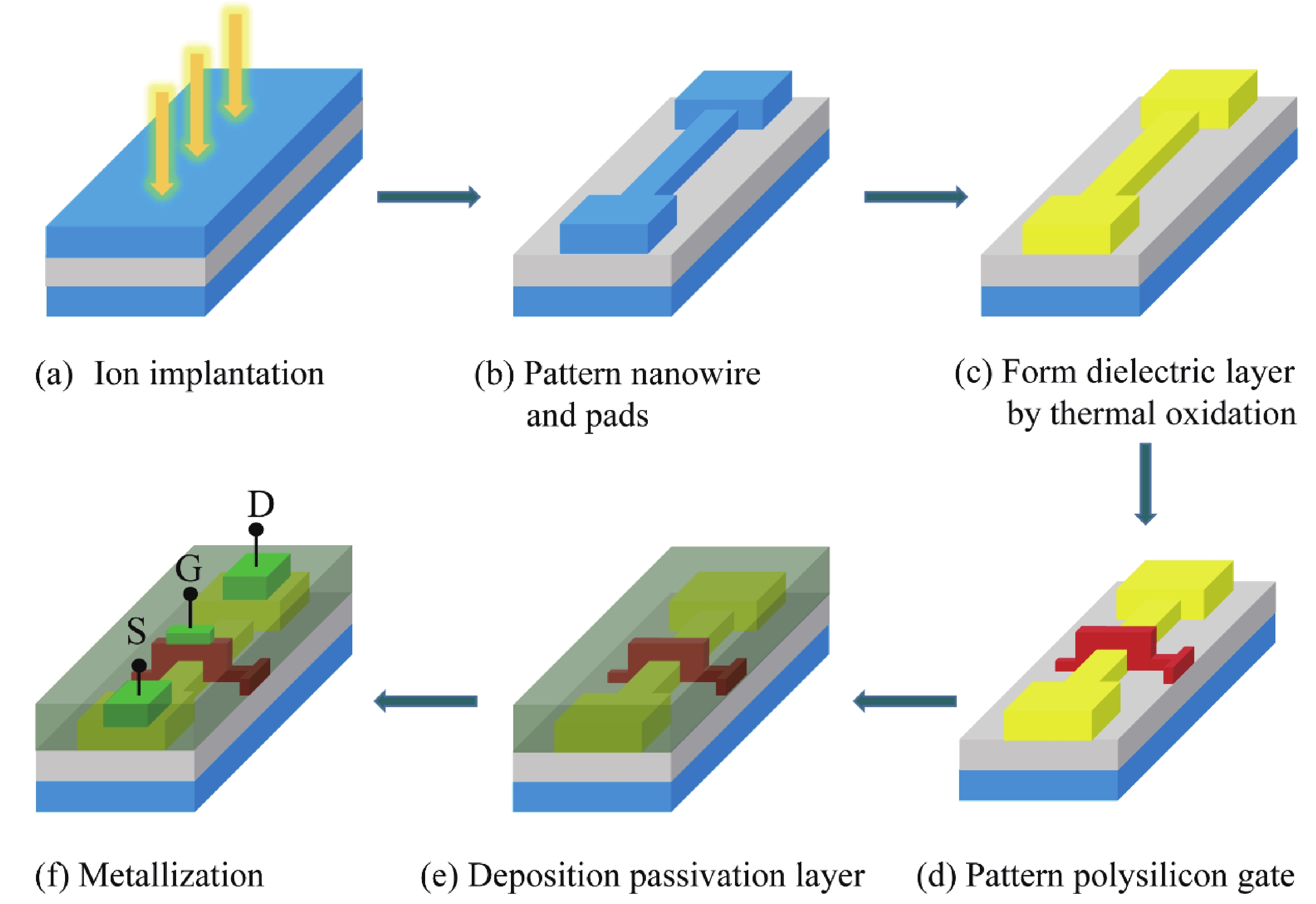
Fig. 1.
(Color online) Schematic diagrams of the fabrication process for JNTs.
ARTICLES
Yifan Fu1, Liuhong Ma1, 2, 3, , Zhiyong Duan1, 4 and Weihua Han2, 3,
Corresponding author: Liuhong Ma, Email: maliuhong@zzu.edu.cn; Weihua Han, Email: weihua@semi.ac.cn
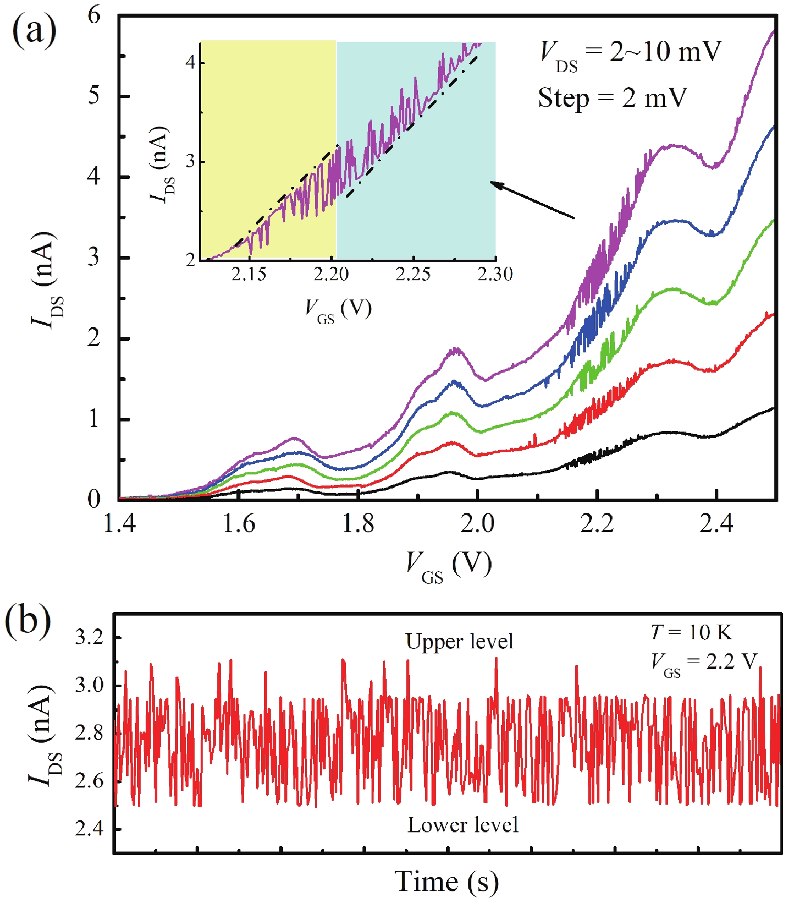
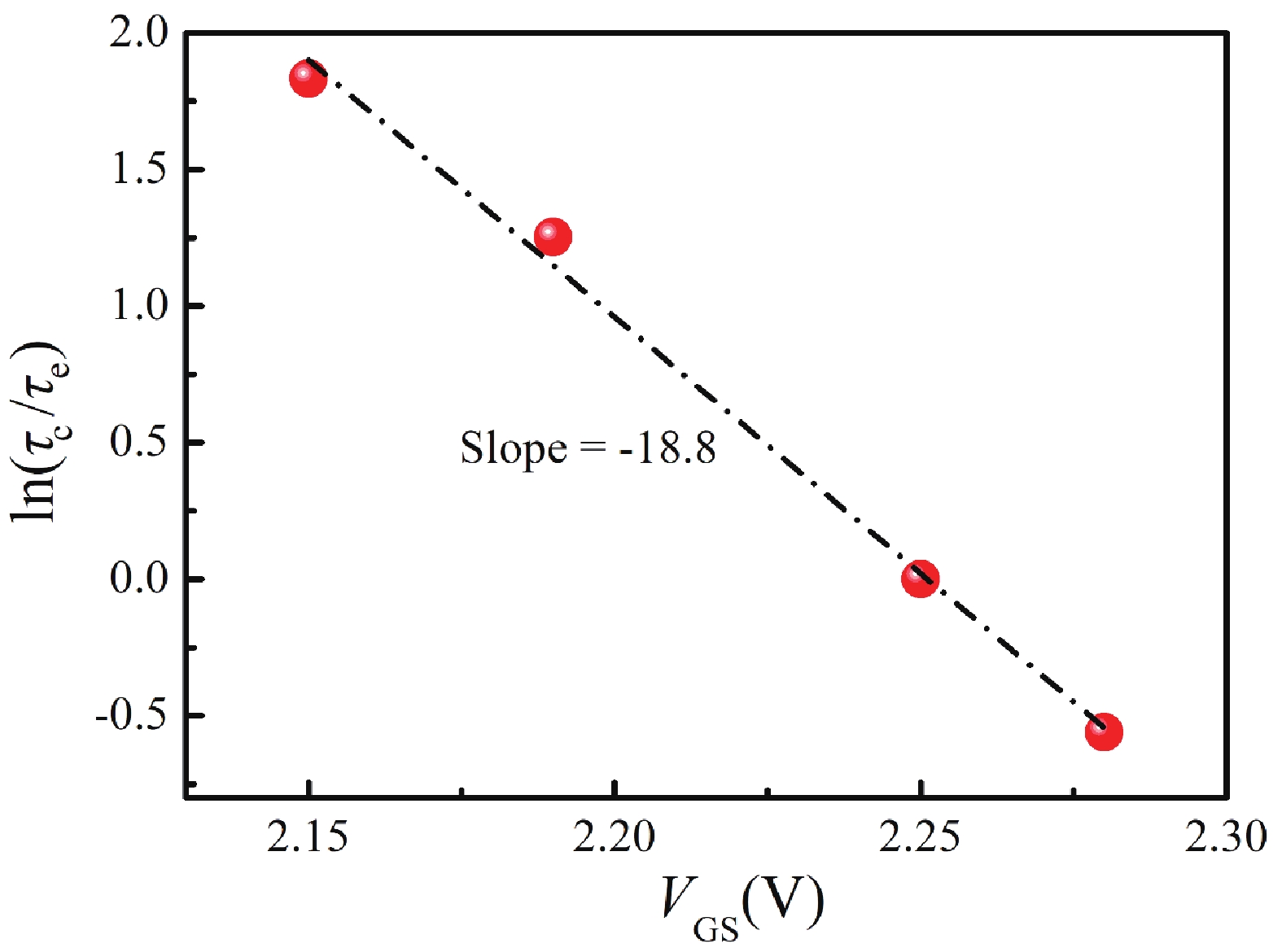
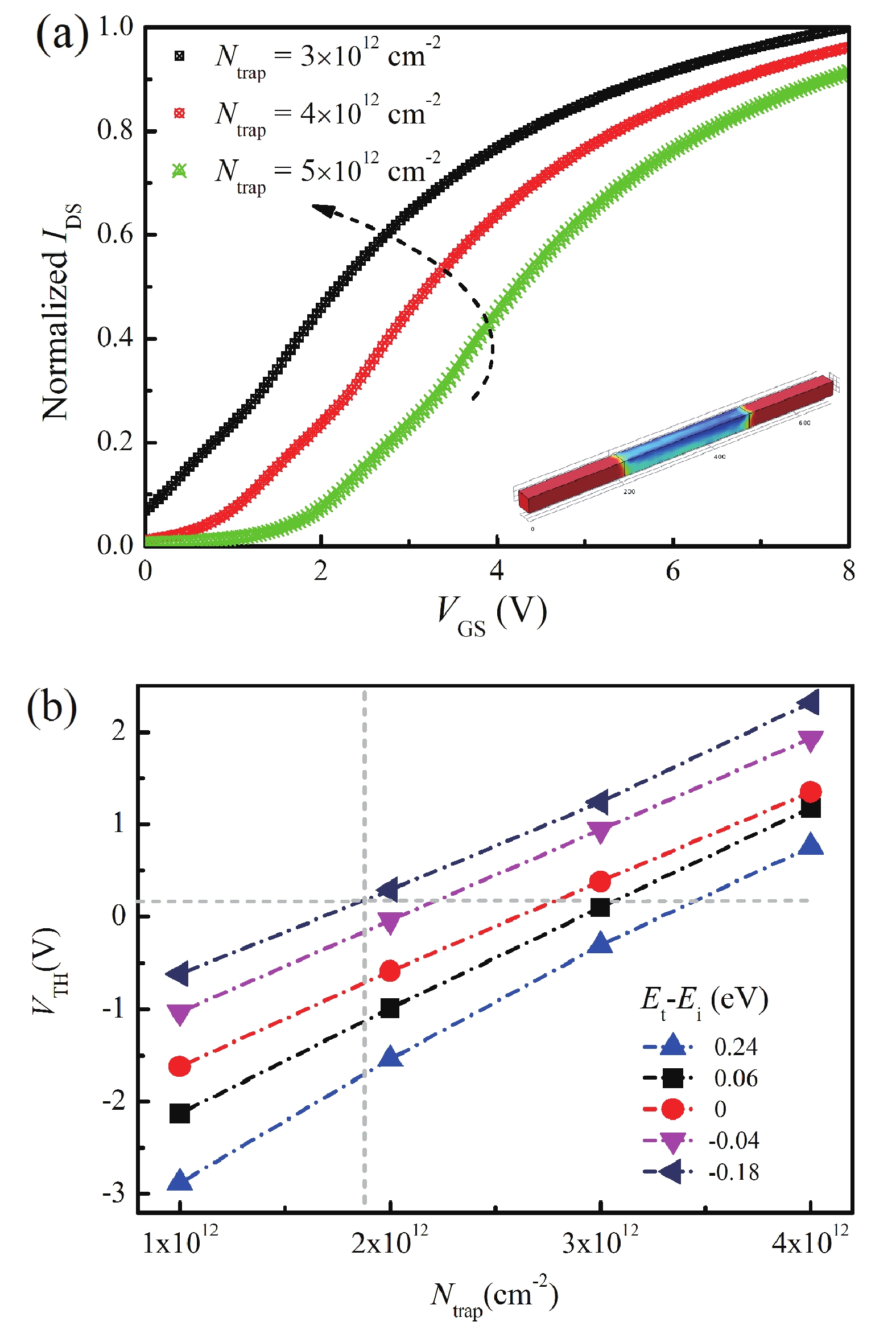
Abstract: We investigated the effect of charge trapping on electrical characteristics of silicon junctionless nanowire transistors which are fabricated on heavily n-type doped silicon-on-insulator substrate. The obvious random telegraph noise and current hysteresis observed at the temperature of 10 K indicate the existence of acceptor-like traps. The position depth of the traps in the oxide from Si/SiO2 interface is 0.35 nm, calculated by utilizing the dependence of the capture and emission time on the gate voltage. Moreover, by constructing a three-dimensional model of tri-gate device structure in COMSOL Multiphysics simulation software, we achieved the trap density of 1.9 × 1012 cm–2 and the energy level position of traps at 0.18 eV below the intrinsic Fermi level.
Key words: junctionless transistor, charge trapping, random telegraph signals
| [1] |
Zhou W H, Zhang S L, Guo S Y, et al. Designing sub-10-nm metal-oxide-semiconductor field-effect transistors via ballistic transport and disparate effective mass: The case of two-dimensional BiN. Phys Rev Appl, 2020, 13(4), 044066 doi: 10.1103/PhysRevApplied.13.044066
|
| [2] |
Zhou W H, Zhang S L, Wang Y Y. Anisotropic in-plane ballistic transport in monolayer black arsenic-phosphorus FETs. Adv Electron Mater, 2020, 6(3), 1901281 doi: 10.1002/aelm.201901281
|
| [3] |
Jeon D Y, Mouis M, Barraud S, et al. Channel width dependent subthreshold operation of tri-gate junctionless transistors. Solid-State Electron, 2020, 171, 107860 doi: 10.1016/j.sse.2020.107860
|
| [4] |
Colinge J P, Lee C W, Afzalian A, et al. Nanowire transistors without junctions. Nat Nanotechnol, 2010, 5, 225 doi: 10.1038/nnano.2010.15
|
| [5] |
Mendiratta N, Tripathi S L. A review on performance comparison of advanced MOSFET structures below 45 nm technology node. J Semicond, 2020, 41(6), 061401 doi: 10.1088/1674-4926/41/6/061401
|
| [6] |
Lee J, Kim Y, Cho S. Design of poly-Si junctionless Fin-channel FET with quantum-mechanical drift-diffusion models for sub-10-nm technology nodes. IEEE Trans Electron Dev, 2016, 63, 4610 doi: 10.1109/TED.2016.2614990
|
| [7] |
Yan R, Kranti A, Ferain I, et al. Investigation of high-performance sub-50 nm junctionless nanowire transistors. Microelectron Reliab, 2011, 51(7), 1166 doi: 10.1016/j.microrel.2011.02.016
|
| [8] |
Rudenko T, Nazarov A, Ferain I, et al. Mobility enhancement effect in heavily doped junctionless nanowire silicon-on-insulator metal-oxide-semiconductor field-effect transistors. Appl Phys Lett, 2012, 101, 053511 doi: 10.1063/1.4767353
|
| [9] |
Gupta S, Nigam K, Pandey S, et al. Effect of interface trap charges on performance variation of heterogeneous gate dielectric junctionless-TFET. IEEE Trans Electron Dev, 2017, 64(11), 1 doi: 10.1109/TED.2017.2754297
|
| [10] |
Nazarov A N, Ferain I, Akhavan N D, et al. Random telegraph-signal noise in junctionless transistors. Appl Phys Lett, 2011, 98(9), 092111 doi: 10.1063/1.3557505
|
| [11] |
Berengue O M, Chiquito J. Direct evidence of traps controlling the carriers transport in SnO2 nanobelts. J Semicond, 2017, 38(12), 122001 doi: 10.1088/1674-4926/38/12/122001
|
| [12] |
Ma L H, Han W H, Wang H, et al. Charge trapping in surface accumulation layer of heavily doped junctionless nanowire transistors. Chin Phys B, 2015, 024(012), 589 doi: 10.1088/1674-1056/24/12/128101
|
| [13] |
Hu G X, Hu S Y, Feng J H, et al. Analytical models for channel potential, threshold voltage, and subthreshold swing of junctionless triple-gate FinFETs. Microelectron J, 2016, 50, 60 doi: 10.1016/j.mejo.2016.02.003
|
| [14] |
Liu F Y, Liu H Z, Liu B W, et al. An analytical model for nanowire junctionless SOI FinFETs with considering three-dimensional coupling effect. Chin Phys B, 2016, 25(4), 047305 doi: 10.1088/1674-1056/25/4/047305
|
| [15] |
ávila-Herreraa F, Pazb B C, Cerdeira A. Charge-based compact analytical model for triple-gate junctionless nanowire transistors. Solid-State Electron, 2016, 122(1), 23 doi: 10.1016/j.sse.2016.04.013
|
| [16] |
Liang Y Y, Jang Kyungsoo, Velumani S, et al. Effects of interface trap density on the electrical performance of amorphous InSnZnO thin-film transistor. J Semicond, 2015, 36(2), 024007 doi: 10.1088/1674-4926/36/2/024007
|
| [17] |
Liu F, Wang K L, Li C, et al. Study of random telegraph signals in single-walled carbon nanotube field effect transistors. IEEE Trans Nanotechnol, 2006, 5(5), 441 doi: 10.1109/TNANO.2006.880906
|
| [18] |
Sun Y, Zhang L N, Ahmed Z, et al. Characterization of interface trap dynamics responsible for hysteresis in organic thin-film transistors. Org Electron, 2015, 27, 192 doi: 10.1016/j.orgel.2015.09.011
|
| [19] |
Amarasinghe N V, Elik-Butler Z, Vasina P, et al. Characterization of oxide traps in 0.15 μm2 MOSFETs using random telegraph signals. Microelectron Reliab, 2000, 40(11), 1875 doi: 10.1016/S0026-2714(00)00089-5
|
| [20] |
Celik-Butler Z, Vasina P. A method for locating the position of oxide traps responsible for random telegraph signals in submicron MOSFETs. IEEE Trans Electron Dev, 2000, 47(3), 646 doi: 10.1109/16.824742
|
| [21] |
Cheng Y C, Chen H B, Han M H, et al. Temperature dependence of electronic behaviors in quantum dimension junctionless thin-film transistor. Nanoscale Res Lett, 2014, 9(1), 1 doi: 10.1186/1556-276X-9-392
|


Article views: 1930 Times PDF downloads: 139 Times Cited by: 0 Times
Received: 24 December 2021 Revised: 21 January 2022 Online: Accepted Manuscript: 08 April 2022Uncorrected proof: 11 April 2022Published: 01 May 2022
| Citation: |
Yifan Fu, Liuhong Ma, Zhiyong Duan, Weihua Han. Effect of charge trapping on electrical characteristics of silicon junctionless nanowire transistor[J]. Journal of Semiconductors, 2022, 43(5): 054101. doi: 10.1088/1674-4926/43/5/054101
****
Y F Fu, L H Ma, Z Y Duan, W H Han. Effect of charge trapping on electrical characteristics of silicon junctionless nanowire transistor[J]. J. Semicond, 2022, 43(5): 054101. doi: 10.1088/1674-4926/43/5/054101

|
| [1] |
Zhou W H, Zhang S L, Guo S Y, et al. Designing sub-10-nm metal-oxide-semiconductor field-effect transistors via ballistic transport and disparate effective mass: The case of two-dimensional BiN. Phys Rev Appl, 2020, 13(4), 044066 doi: 10.1103/PhysRevApplied.13.044066
|
| [2] |
Zhou W H, Zhang S L, Wang Y Y. Anisotropic in-plane ballistic transport in monolayer black arsenic-phosphorus FETs. Adv Electron Mater, 2020, 6(3), 1901281 doi: 10.1002/aelm.201901281
|
| [3] |
Jeon D Y, Mouis M, Barraud S, et al. Channel width dependent subthreshold operation of tri-gate junctionless transistors. Solid-State Electron, 2020, 171, 107860 doi: 10.1016/j.sse.2020.107860
|
| [4] |
Colinge J P, Lee C W, Afzalian A, et al. Nanowire transistors without junctions. Nat Nanotechnol, 2010, 5, 225 doi: 10.1038/nnano.2010.15
|
| [5] |
Mendiratta N, Tripathi S L. A review on performance comparison of advanced MOSFET structures below 45 nm technology node. J Semicond, 2020, 41(6), 061401 doi: 10.1088/1674-4926/41/6/061401
|
| [6] |
Lee J, Kim Y, Cho S. Design of poly-Si junctionless Fin-channel FET with quantum-mechanical drift-diffusion models for sub-10-nm technology nodes. IEEE Trans Electron Dev, 2016, 63, 4610 doi: 10.1109/TED.2016.2614990
|
| [7] |
Yan R, Kranti A, Ferain I, et al. Investigation of high-performance sub-50 nm junctionless nanowire transistors. Microelectron Reliab, 2011, 51(7), 1166 doi: 10.1016/j.microrel.2011.02.016
|
| [8] |
Rudenko T, Nazarov A, Ferain I, et al. Mobility enhancement effect in heavily doped junctionless nanowire silicon-on-insulator metal-oxide-semiconductor field-effect transistors. Appl Phys Lett, 2012, 101, 053511 doi: 10.1063/1.4767353
|
| [9] |
Gupta S, Nigam K, Pandey S, et al. Effect of interface trap charges on performance variation of heterogeneous gate dielectric junctionless-TFET. IEEE Trans Electron Dev, 2017, 64(11), 1 doi: 10.1109/TED.2017.2754297
|
| [10] |
Nazarov A N, Ferain I, Akhavan N D, et al. Random telegraph-signal noise in junctionless transistors. Appl Phys Lett, 2011, 98(9), 092111 doi: 10.1063/1.3557505
|
| [11] |
Berengue O M, Chiquito J. Direct evidence of traps controlling the carriers transport in SnO2 nanobelts. J Semicond, 2017, 38(12), 122001 doi: 10.1088/1674-4926/38/12/122001
|
| [12] |
Ma L H, Han W H, Wang H, et al. Charge trapping in surface accumulation layer of heavily doped junctionless nanowire transistors. Chin Phys B, 2015, 024(012), 589 doi: 10.1088/1674-1056/24/12/128101
|
| [13] |
Hu G X, Hu S Y, Feng J H, et al. Analytical models for channel potential, threshold voltage, and subthreshold swing of junctionless triple-gate FinFETs. Microelectron J, 2016, 50, 60 doi: 10.1016/j.mejo.2016.02.003
|
| [14] |
Liu F Y, Liu H Z, Liu B W, et al. An analytical model for nanowire junctionless SOI FinFETs with considering three-dimensional coupling effect. Chin Phys B, 2016, 25(4), 047305 doi: 10.1088/1674-1056/25/4/047305
|
| [15] |
ávila-Herreraa F, Pazb B C, Cerdeira A. Charge-based compact analytical model for triple-gate junctionless nanowire transistors. Solid-State Electron, 2016, 122(1), 23 doi: 10.1016/j.sse.2016.04.013
|
| [16] |
Liang Y Y, Jang Kyungsoo, Velumani S, et al. Effects of interface trap density on the electrical performance of amorphous InSnZnO thin-film transistor. J Semicond, 2015, 36(2), 024007 doi: 10.1088/1674-4926/36/2/024007
|
| [17] |
Liu F, Wang K L, Li C, et al. Study of random telegraph signals in single-walled carbon nanotube field effect transistors. IEEE Trans Nanotechnol, 2006, 5(5), 441 doi: 10.1109/TNANO.2006.880906
|
| [18] |
Sun Y, Zhang L N, Ahmed Z, et al. Characterization of interface trap dynamics responsible for hysteresis in organic thin-film transistors. Org Electron, 2015, 27, 192 doi: 10.1016/j.orgel.2015.09.011
|
| [19] |
Amarasinghe N V, Elik-Butler Z, Vasina P, et al. Characterization of oxide traps in 0.15 μm2 MOSFETs using random telegraph signals. Microelectron Reliab, 2000, 40(11), 1875 doi: 10.1016/S0026-2714(00)00089-5
|
| [20] |
Celik-Butler Z, Vasina P. A method for locating the position of oxide traps responsible for random telegraph signals in submicron MOSFETs. IEEE Trans Electron Dev, 2000, 47(3), 646 doi: 10.1109/16.824742
|
| [21] |
Cheng Y C, Chen H B, Han M H, et al. Temperature dependence of electronic behaviors in quantum dimension junctionless thin-film transistor. Nanoscale Res Lett, 2014, 9(1), 1 doi: 10.1186/1556-276X-9-392
|

 WeChat ID
Journal of Semiconductors © 2017 All Rights Reserved 京ICP備05085259號-2
 DownLoad:

