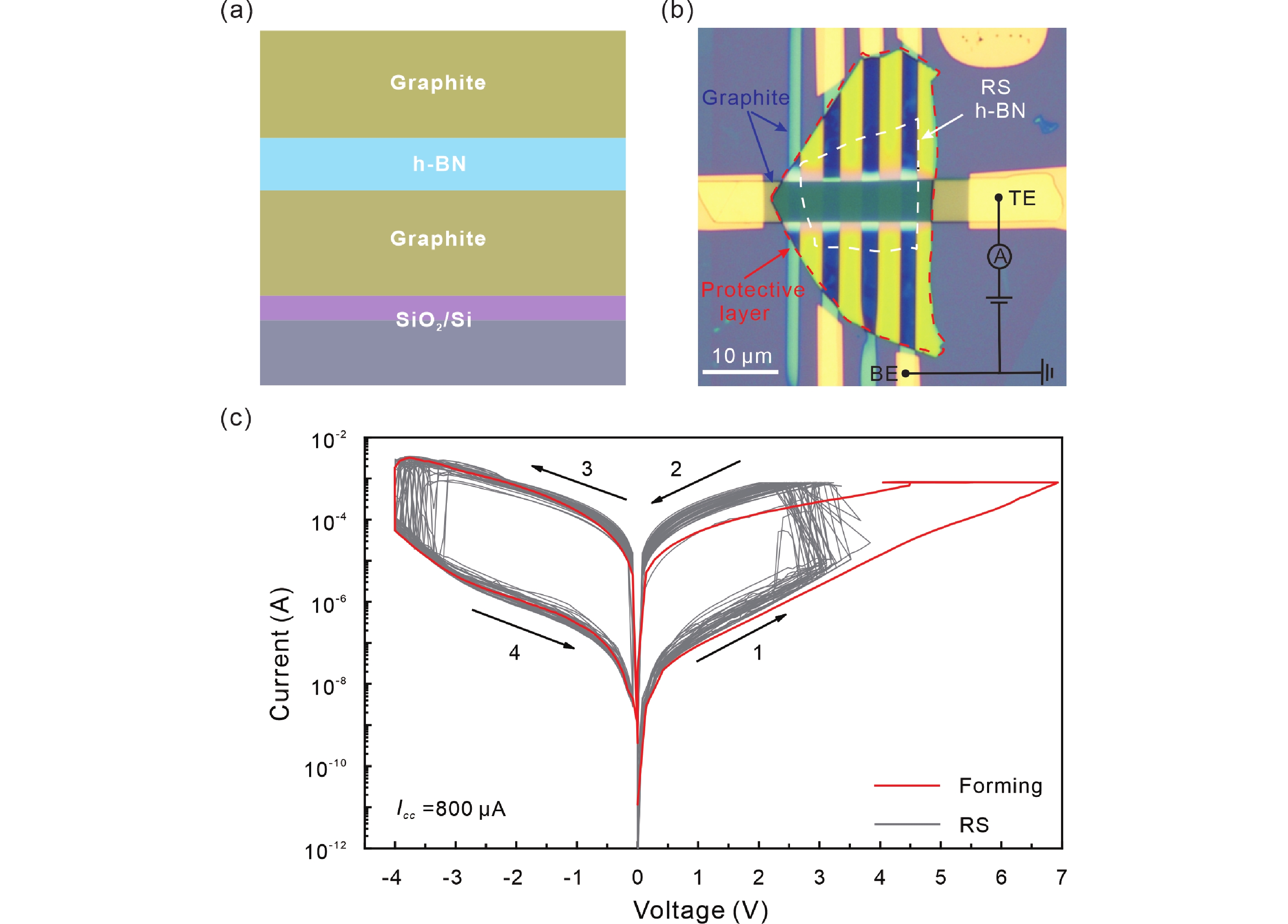
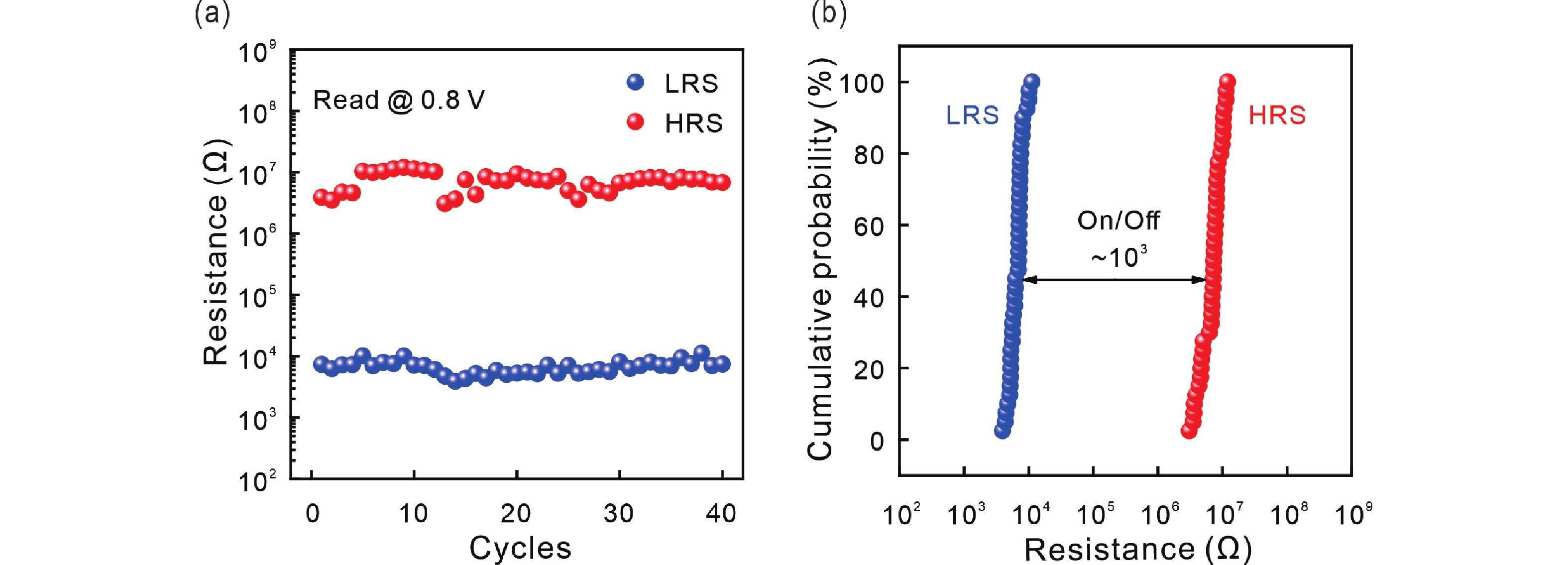
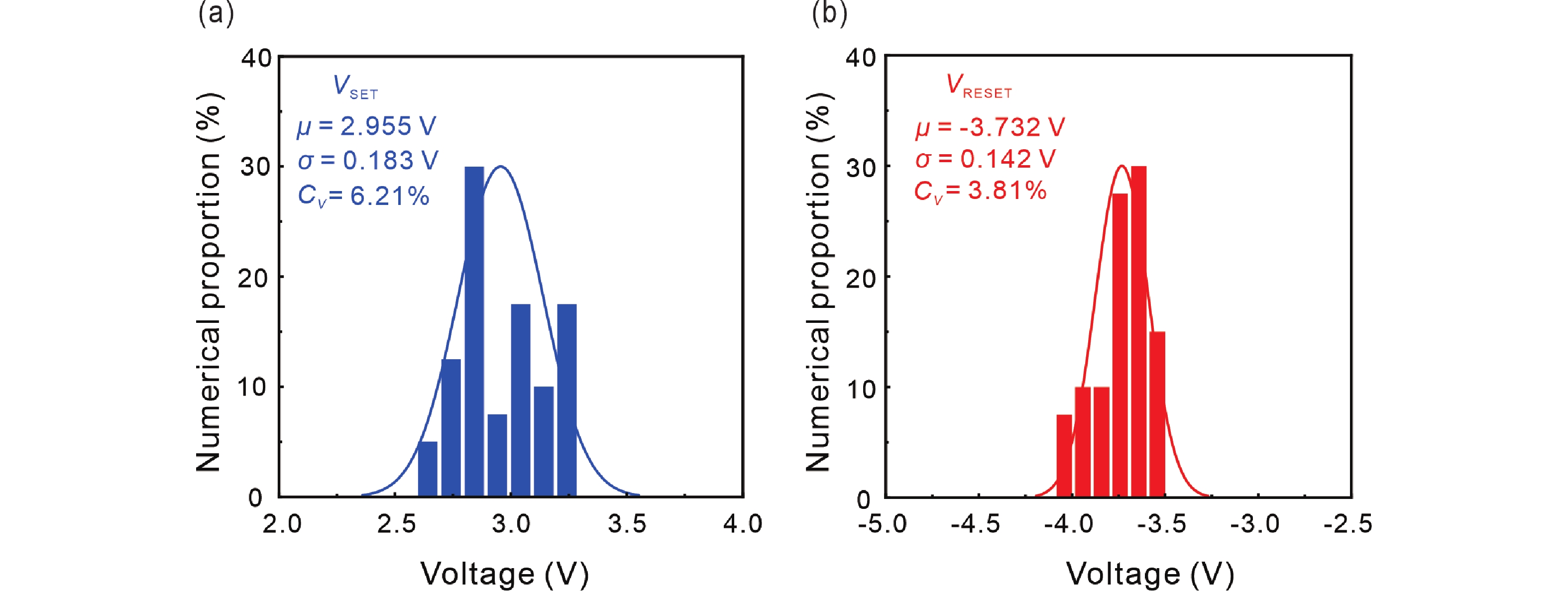
ARTICLES
Yafeng Deng1, ?, Yixiang Li2, ?, , Pengfei Wang2, Shuang Wang2, Xuan Pan2 and Dong Wang1,
Corresponding author: Yixiang Li, liyx@nju.edu.cn; Dong Wang, xjrshwd@henau.edu.cn
Abstract: With the atomically sharp interface and stable switching channel, van der Waals (vdW) heterostructure memristors have attracted extensive interests for the application of high-density memory and neuromorphic computing. Here, we demonstrate a new type of vdW heterostructure memristor device by sandwiching a single-crystalline h-BN layer between two thin graphites. In such a device, a stable bipolar resistive switching (RS) behavior has been observed for the first time. We also characterize their switching performance, and observe an on/off ratio of >103 and a minimum RESET voltage variation coefficient of 3.81%. Our work underscores the potential of 2D materials and vdW heterostructures for emerging memory and neuromorphic applications.
Key words: hexagonal boron nitride, van der Waals heterostructure, memristor
| [1] |
Wang J, Ma F, Liang W, et al. Electrical properties and applications of graphene, hexagonal boron nitride (h-BN), and graphene/h-BN heterostructures. Mater Today Phys, 2017, 2, 6 doi: 10.1016/j.mtphys.2017.07.001
|
| [2] |
Ranjan A, Raghavan N, O'Shea S J, et al. Conductive atomic force microscope study of bipolar and threshold resistive switching in 2D hexagonal boron nitride films. Sci Rep, 2018, 8, 2854 doi: 10.1038/s41598-018-21138-x
|
| [3] |
Qian K, Tay R Y, Nguyen V C, et al. Hexagonal boron nitride thin film for flexible resistive memory applications. Adv Funct Mater, 2016, 26, 2176 doi: 10.1002/adfm.201504771
|
| [4] |
Roy S, Zhang X, Puthirath A B, et al. Structure, properties and applications of two-dimensional hexagonal boron nitride. Adv Mater, 2021, 33, 2101589 doi: 10.1002/adma.202101589
|
| [5] |
Ahmed F, Heo S, Yang Z, et al. Dielectric dispersion and high field response of multilayer hexagonal boron nitride. Adv Funct Mater, 2018, 28, 1804235 doi: 10.1002/adfm.201804235
|
| [6] |
Gani Y S, Abergel D S L, and Rossi E. Electronic structure of graphene nanoribbons on hexagonal boron nitride. Phys Rev B, 2018, 98, 205415 doi: 10.1103/PhysRevB.98.205415
|
| [7] |
Lee G H, Yu Y J, Lee C, et al. Electron tunneling through atomically flat and ultrathin hexagonal boron nitride. Appl Phys Lett, 2011, 99, 243114 doi: 10.1063/1.3662043
|
| [8] |
Pan C, Ji Y, Xiao N, et al. Coexistence of grain-boundaries-assisted bipolar and threshold resistive switching in multilayer hexagonal boron nitride. Adv Funct Mater, 2017, 27, 1604811 doi: 10.1002/adfm.201604811
|
| [9] |
Yuan B, Liang X, Zhong L, et al. 150 nm × 200 nm cross-point hexagonal boron nitride-based memristors. Adv Electron Mater, 2020, 6, 1900115 doi: 10.1002/aelm.201900115
|
| [10] |
Zhao H, Dong Z, Tian H, et al. Atomically thin femtojoule memristive device. Adv Mater, 2017, 29, 1703232 doi: 10.1002/adma.201703232
|
| [11] |
Zhu K, Liang X, Yuan B, et al. Graphene-boron nitride-graphene cross-point memristors with three stable resistive states. ACS Appl Mater Interfaces, 2019, 11, 37999 doi: 10.1021/acsami.9b04412
|
| [12] |
Wu X, Ge R, Chen P A, et al. Thinnest nonvolatile memory based on monolayer h-BN. Adv Mater, 2019, 31, 1806790 doi: 10.1002/adma.201806790
|
| [13] |
Zhao Q, Xie Z, Peng Y P, et al. Current status and prospects of memristors based on novel 2D materials. Mater Horiz, 2020, 7, 1495 doi: 10.1039/C9MH02033K
|
| [14] |
Wang C Y, Wang C, Meng F, et al. 2D layered materials for memristive and neuromorphic applications. Adv Electron Mater, 2019, 6, 1901107 doi: 10.1002/aelm.201901107
|
| [15] |
Shi T, Wang R, Wu Z, et al. A review of resistive switching devices: Performance improvement, characterization, and applications. Small Struct, 2021, 2, 2000109 doi: 10.1002/sstr.202000109
|
| [16] |
Huh W, Lee D, and Lee C H. Memristors based on 2D materials as an artificial synapse for neuromorphic electronics. Adv Mater, 2020, 32, 2002092 doi: 10.1002/adma.202002092
|
| [17] |
Tao Q, Wu R, Li Q, et al. Reconfigurable electronics by disassembling and reassembling van der waals heterostructures. Nat Commun, 2021, 12, 1825 doi: 10.1038/s41467-021-22118-y
|
| [18] |
Li S, Pam M E, Li Y, et al. Wafer-scale 2D hafnium diselenide based memristor crossbar array for energy-efficient neural network hardware. Adv Mater, 2021, 33, 2103376 doi: 10.1002/adma.202103376
|
| [19] |
Sun L, Zhang Y, Han G, et al. Self-selective van der waals heterostructures for large scale memory array. Nat Commun, 2019, 10, 3161 doi: 10.1038/s41467-019-11187-9
|
| [20] |
Wang S, Wang C Y, Wang P, et al. Networking retinomorphic sensor with memristive crossbar for brain-inspired visual perception. Nat Sci Rev, 2021, 8, 172 doi: 10.1093/nsr/nwaa172
|
| [21] |
Jain N, Yang F, Jacobs-Gedrim R B, et al. Extenuated interlayer scattering in double-layered graphene/hexagonal boron nitride heterostructure. Carbon, 2018, 126, 17 doi: 10.1016/j.carbon.2017.09.074
|
| [22] |
Wang H, Yu T, Zhao J, et al. Low-power memristors based on layered 2D SnSe/graphene materials. Sci China Mater, 2021, 64, 198 doi: 10.1007/s40843-020-1358-5
|
| [23] |
He H K, Yang F F, and Yang R. Flexible full two-dimensional memristive synapses of graphene/WSe2 – xO y/graphene. Phys Chem Chem Phys, 2020, 22, 20658 doi: 10.1039/D0CP03822A
|
| [24] |
Wang M, Cai S, Pan C, et al. Robust memristors based on layered two-dimensional materials. Nat Electron, 2018, 1, 130 doi: 10.1038/s41928-018-0021-4
|
| [25] |
Liu C, Chen H, Wang S, et al. Two-dimensional materials for next-generation computing technologies. Nat Nanotechnol, 2020, 15, 545 doi: 10.1038/s41565-020-0724-3
|
| [26] |
Hao Y, Wu H, Yang Y, et al. Preface to the special issue on beyond moore: Resistive switching devices for emerging memory and neuromorphic computing. J Semicond, 2021, 42, 010101 doi: 10.1088/1674-4926/42/1/010101
|
| [27] |
Shen Y, Zheng W, Zhu K, et al. Variability and yield in h-BN-based memristive circuits: The role of each type of defect. Adv Mater, 2021, 33, 2103656 doi: 10.1002/adma.202103656
|
| [28] |
Zhou Z, Zhao J, Chen A P, et al. Designing carbon conductive filament memristor devices for memory and electronic synapse applications. Mater Horiz, 2020, 7, 1106 doi: 10.1039/C9MH01684H
|
| [29] |
Standley B, Bao W Z, Zhang H, et al. Graphene-based atomic-scale switches. Nano Lett, 2008, 8, 3345 doi: 10.1021/nl801774a
|
| [30] |
Hattori Y, Taniguchi T, Watanabe K, et al. Layer-by-layer dielectric breakdown of hexagonal boron nitride. ACS Nano, 2015, 9, 916 doi: 10.1021/nn506645q
|
| [31] |
Ranjan A, Raghavan N, Puglisi F M, et al. Boron vacancies causing breakdown in 2D layered hexagonal boron nitride dielectrics. IEEE Electron Device Lett, 2019, 40, 1321 doi: 10.1109/LED.2019.2923420
|
| [32] |
Jin C, Lin F, Suenaga K, et al. Fabrication of a freestanding boron nitride single layer and its defect assignments. Phys Rev Lett, 2009, 102, 195505 doi: 10.1103/PhysRevLett.102.195505
|
| [33] |
Weston L, Wickramaratne D, Mackoit M, et al. Native point defects and impurities in hexagonal boron nitride. Phys Rev B, 2018, 97, 214104 doi: 10.1103/PhysRevB.97.214104
|
| [34] |
Zobelli A, Ewels C P, Gloter A, et al. Vacancy migration in hexagonal boron nitride. Phys Rev B, 2007, 75, 094104 doi: 10.1103/PhysRevB.75.094104
|
Article views: 2534 Times PDF downloads: 159 Times Cited by: 0 Times
Received: 19 October 2021 Revised: 30 October 2021 Online: Accepted Manuscript: 23 December 2021Uncorrected proof: 30 December 2021Published: 01 May 2022
| Citation: |
Yafeng Deng, Yixiang Li, Pengfei Wang, Shuang Wang, Xuan Pan, Dong Wang. Observation of resistive switching in a graphite/hexagonal boron nitride/graphite heterostructure memristor[J]. Journal of Semiconductors, 2022, 43(5): 052003. doi: 10.1088/1674-4926/43/5/052003
****
Y F Deng, Y X Li, P F Wang, S Wang, X Pan, D Wang. Observation of resistive switching in a graphite/hexagonal boron nitride/graphite heterostructure memristor[J]. J. Semicond, 2022, 43(5): 052003. doi: 10.1088/1674-4926/43/5/052003
|
| [1] |
Wang J, Ma F, Liang W, et al. Electrical properties and applications of graphene, hexagonal boron nitride (h-BN), and graphene/h-BN heterostructures. Mater Today Phys, 2017, 2, 6 doi: 10.1016/j.mtphys.2017.07.001
|
| [2] |
Ranjan A, Raghavan N, O'Shea S J, et al. Conductive atomic force microscope study of bipolar and threshold resistive switching in 2D hexagonal boron nitride films. Sci Rep, 2018, 8, 2854 doi: 10.1038/s41598-018-21138-x
|
| [3] |
Qian K, Tay R Y, Nguyen V C, et al. Hexagonal boron nitride thin film for flexible resistive memory applications. Adv Funct Mater, 2016, 26, 2176 doi: 10.1002/adfm.201504771
|
| [4] |
Roy S, Zhang X, Puthirath A B, et al. Structure, properties and applications of two-dimensional hexagonal boron nitride. Adv Mater, 2021, 33, 2101589 doi: 10.1002/adma.202101589
|
| [5] |
Ahmed F, Heo S, Yang Z, et al. Dielectric dispersion and high field response of multilayer hexagonal boron nitride. Adv Funct Mater, 2018, 28, 1804235 doi: 10.1002/adfm.201804235
|
| [6] |
Gani Y S, Abergel D S L, and Rossi E. Electronic structure of graphene nanoribbons on hexagonal boron nitride. Phys Rev B, 2018, 98, 205415 doi: 10.1103/PhysRevB.98.205415
|
| [7] |
Lee G H, Yu Y J, Lee C, et al. Electron tunneling through atomically flat and ultrathin hexagonal boron nitride. Appl Phys Lett, 2011, 99, 243114 doi: 10.1063/1.3662043
|
| [8] |
Pan C, Ji Y, Xiao N, et al. Coexistence of grain-boundaries-assisted bipolar and threshold resistive switching in multilayer hexagonal boron nitride. Adv Funct Mater, 2017, 27, 1604811 doi: 10.1002/adfm.201604811
|
| [9] |
Yuan B, Liang X, Zhong L, et al. 150 nm × 200 nm cross-point hexagonal boron nitride-based memristors. Adv Electron Mater, 2020, 6, 1900115 doi: 10.1002/aelm.201900115
|
| [10] |
Zhao H, Dong Z, Tian H, et al. Atomically thin femtojoule memristive device. Adv Mater, 2017, 29, 1703232 doi: 10.1002/adma.201703232
|
| [11] |
Zhu K, Liang X, Yuan B, et al. Graphene-boron nitride-graphene cross-point memristors with three stable resistive states. ACS Appl Mater Interfaces, 2019, 11, 37999 doi: 10.1021/acsami.9b04412
|
| [12] |
Wu X, Ge R, Chen P A, et al. Thinnest nonvolatile memory based on monolayer h-BN. Adv Mater, 2019, 31, 1806790 doi: 10.1002/adma.201806790
|
| [13] |
Zhao Q, Xie Z, Peng Y P, et al. Current status and prospects of memristors based on novel 2D materials. Mater Horiz, 2020, 7, 1495 doi: 10.1039/C9MH02033K
|
| [14] |
Wang C Y, Wang C, Meng F, et al. 2D layered materials for memristive and neuromorphic applications. Adv Electron Mater, 2019, 6, 1901107 doi: 10.1002/aelm.201901107
|
| [15] |
Shi T, Wang R, Wu Z, et al. A review of resistive switching devices: Performance improvement, characterization, and applications. Small Struct, 2021, 2, 2000109 doi: 10.1002/sstr.202000109
|
| [16] |
Huh W, Lee D, and Lee C H. Memristors based on 2D materials as an artificial synapse for neuromorphic electronics. Adv Mater, 2020, 32, 2002092 doi: 10.1002/adma.202002092
|
| [17] |
Tao Q, Wu R, Li Q, et al. Reconfigurable electronics by disassembling and reassembling van der waals heterostructures. Nat Commun, 2021, 12, 1825 doi: 10.1038/s41467-021-22118-y
|
| [18] |
Li S, Pam M E, Li Y, et al. Wafer-scale 2D hafnium diselenide based memristor crossbar array for energy-efficient neural network hardware. Adv Mater, 2021, 33, 2103376 doi: 10.1002/adma.202103376
|
| [19] |
Sun L, Zhang Y, Han G, et al. Self-selective van der waals heterostructures for large scale memory array. Nat Commun, 2019, 10, 3161 doi: 10.1038/s41467-019-11187-9
|
| [20] |
Wang S, Wang C Y, Wang P, et al. Networking retinomorphic sensor with memristive crossbar for brain-inspired visual perception. Nat Sci Rev, 2021, 8, 172 doi: 10.1093/nsr/nwaa172
|
| [21] |
Jain N, Yang F, Jacobs-Gedrim R B, et al. Extenuated interlayer scattering in double-layered graphene/hexagonal boron nitride heterostructure. Carbon, 2018, 126, 17 doi: 10.1016/j.carbon.2017.09.074
|
| [22] |
Wang H, Yu T, Zhao J, et al. Low-power memristors based on layered 2D SnSe/graphene materials. Sci China Mater, 2021, 64, 198 doi: 10.1007/s40843-020-1358-5
|
| [23] |
He H K, Yang F F, and Yang R. Flexible full two-dimensional memristive synapses of graphene/WSe2 – xO y/graphene. Phys Chem Chem Phys, 2020, 22, 20658 doi: 10.1039/D0CP03822A
|
| [24] |
Wang M, Cai S, Pan C, et al. Robust memristors based on layered two-dimensional materials. Nat Electron, 2018, 1, 130 doi: 10.1038/s41928-018-0021-4
|
| [25] |
Liu C, Chen H, Wang S, et al. Two-dimensional materials for next-generation computing technologies. Nat Nanotechnol, 2020, 15, 545 doi: 10.1038/s41565-020-0724-3
|
| [26] |
Hao Y, Wu H, Yang Y, et al. Preface to the special issue on beyond moore: Resistive switching devices for emerging memory and neuromorphic computing. J Semicond, 2021, 42, 010101 doi: 10.1088/1674-4926/42/1/010101
|
| [27] |
Shen Y, Zheng W, Zhu K, et al. Variability and yield in h-BN-based memristive circuits: The role of each type of defect. Adv Mater, 2021, 33, 2103656 doi: 10.1002/adma.202103656
|
| [28] |
Zhou Z, Zhao J, Chen A P, et al. Designing carbon conductive filament memristor devices for memory and electronic synapse applications. Mater Horiz, 2020, 7, 1106 doi: 10.1039/C9MH01684H
|
| [29] |
Standley B, Bao W Z, Zhang H, et al. Graphene-based atomic-scale switches. Nano Lett, 2008, 8, 3345 doi: 10.1021/nl801774a
|
| [30] |
Hattori Y, Taniguchi T, Watanabe K, et al. Layer-by-layer dielectric breakdown of hexagonal boron nitride. ACS Nano, 2015, 9, 916 doi: 10.1021/nn506645q
|
| [31] |
Ranjan A, Raghavan N, Puglisi F M, et al. Boron vacancies causing breakdown in 2D layered hexagonal boron nitride dielectrics. IEEE Electron Device Lett, 2019, 40, 1321 doi: 10.1109/LED.2019.2923420
|
| [32] |
Jin C, Lin F, Suenaga K, et al. Fabrication of a freestanding boron nitride single layer and its defect assignments. Phys Rev Lett, 2009, 102, 195505 doi: 10.1103/PhysRevLett.102.195505
|
| [33] |
Weston L, Wickramaratne D, Mackoit M, et al. Native point defects and impurities in hexagonal boron nitride. Phys Rev B, 2018, 97, 214104 doi: 10.1103/PhysRevB.97.214104
|
| [34] |
Zobelli A, Ewels C P, Gloter A, et al. Vacancy migration in hexagonal boron nitride. Phys Rev B, 2007, 75, 094104 doi: 10.1103/PhysRevB.75.094104
|
Journal of Semiconductors © 2017 All Rights Reserved 京ICP備05085259號(hào)-2