


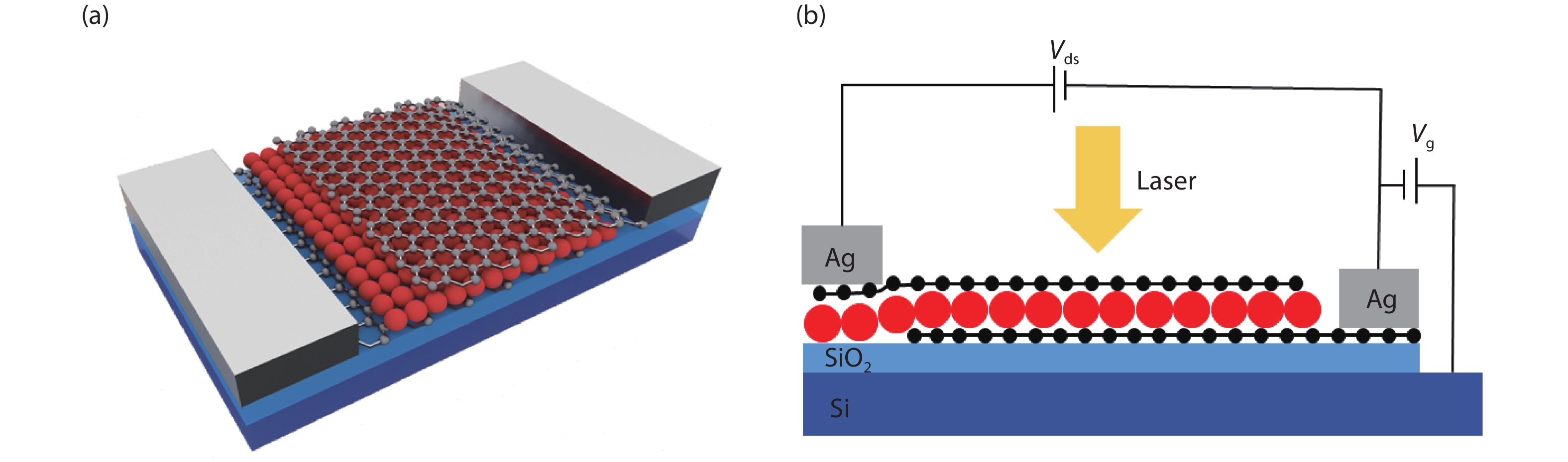
Fig. 1.
(Color online) Device schematic. (a) Device with three-layer structure of graphene/CdSe QDs/graphene, silver as the electrodes on each graphene. (b) Circuit connection diagram of the devices.
ARTICLES
Siyu Zhou1, 2, 3 and Bo Peng1, 2, 3,
Corresponding author: Bo Peng, Email: bo_peng@uestc.edu.cn
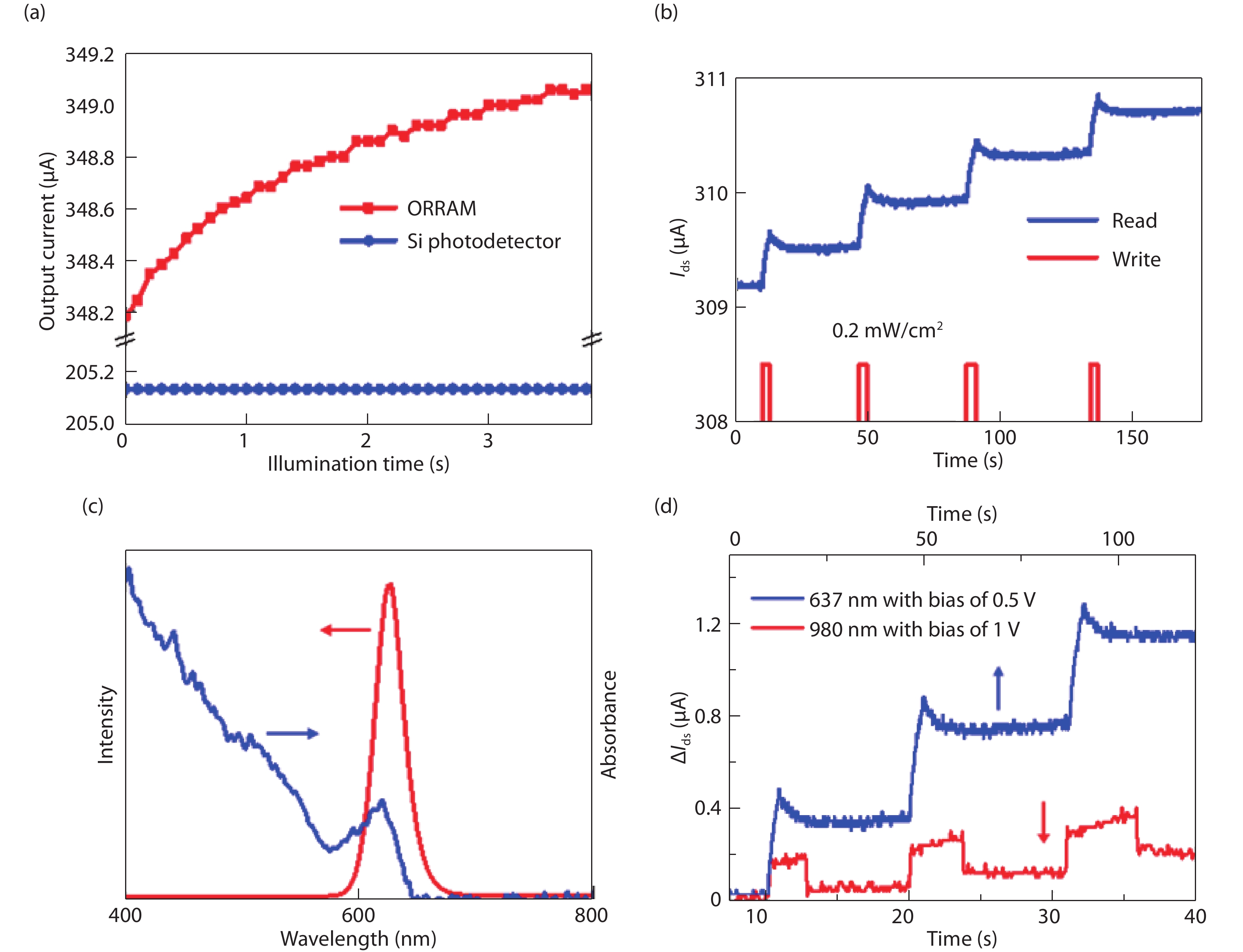
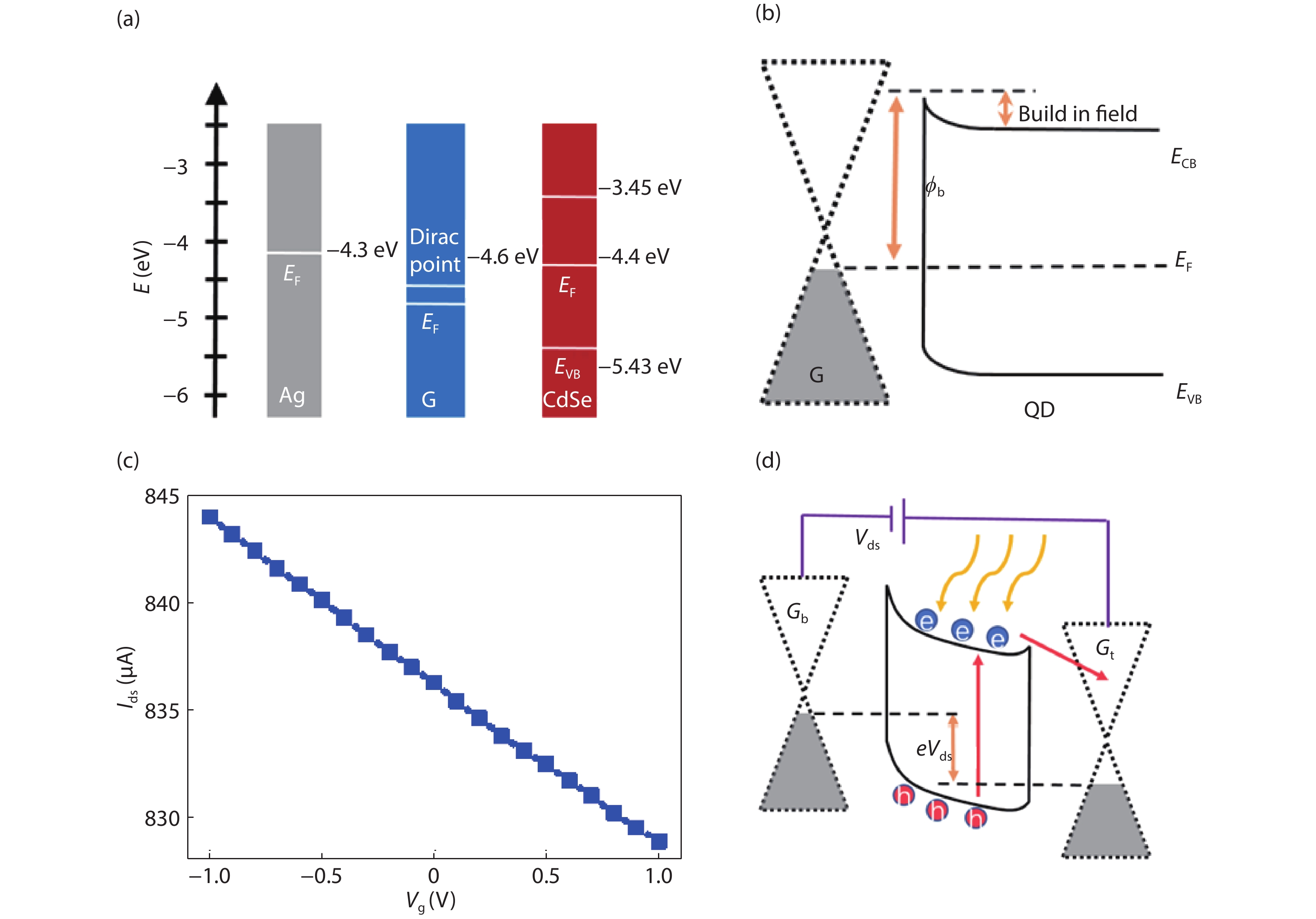
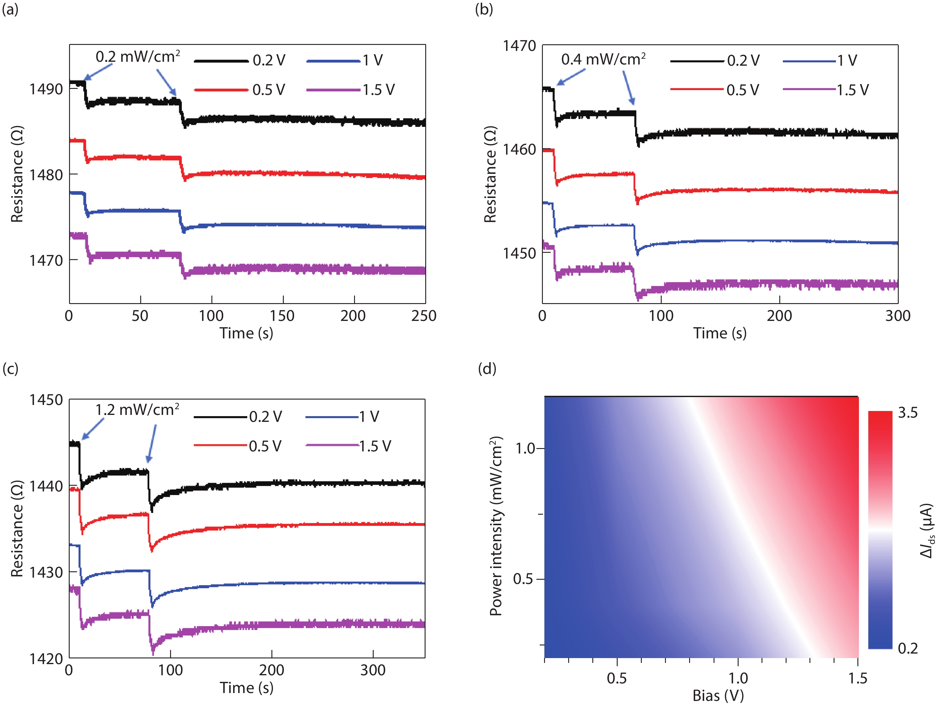
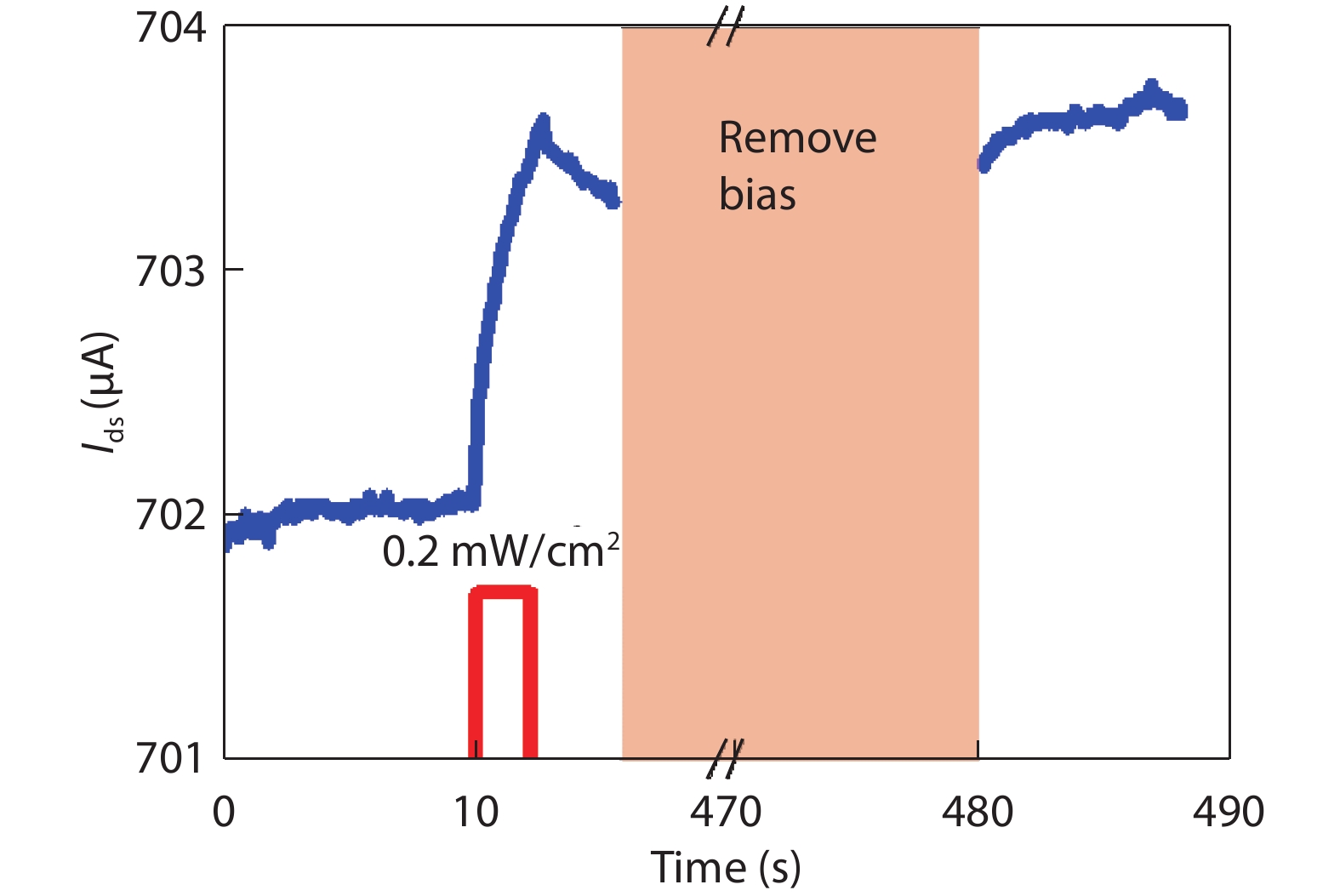
Abstract: Emulating synaptic plasticity in an artificial neural network is crucial to mimic the basic functions of the human brain. In this work, we report a new optoelectronic resistive random access memory (ORRAM) in a three-layer vertical heterostructure of graphene/CdSe quantum dots (QDs)/graphene, which shows non-volatile multi-level optical memory under optical stimuli, giving rise to light-tunable synaptic behaviors. The optical non-volatile storage time is up to ~450 s. The device realizes the function of multi-level optical storage through the interlayer changes between graphene and QDs. This work highlights the feasibility for applying two-dimensional (2D) materials in ORRAM and optoelectronic synaptic devices towards artificial vision.
Key words: ORRAM, heterostructure, synaptic devices
| [1] |
Waldrop M M. The chips are down for Moore’s law. Nature, 2016, 530(7589), 144 doi: 10.1038/530144a
|
| [2] |
Indiveri G, Liu S C. Memory and information processing in neuromorphic systems. Proc IEEE, 2015, 103(8), 1379 doi: 10.1109/JPROC.2015.2444094
|
| [3] |
Cho S, Tan S H, Li Z, et al. SiGe epitaxial memory for neuromorphic computing with reproducible high performance based on engineered dislocations. Nat Mater, 2018, 17(4), 335 doi: 10.1038/s41563-017-0001-5
|
| [4] |
Lü J , Chen Y B , Zuo Z, et al. Charge storage characteristics of nonvolatile floating-gate memory based on gradual Ge1– xSi x/Si heteronanocrystals. J Semicond, 2008, 29(4), 770
|
| [5] |
Zhou H Y, Shi H P, Cheng B C. Surface traps-related nonvolatile resistive switching memory effect in a single SnO2:Sm nanowire. J Semicond, 2020, 41(1), 012101 doi: 10.1088/1674-4926/41/1/012101
|
| [6] |
Shen J, Cong J, Chai Y, et al. Nonvolatile memory based on nonlinear magnetoelectric effects. Phys Rev Appl, 2016, 6(2), 021001 doi: 10.1103/PhysRevApplied.6.021001
|
| [7] |
Shen J, Cong J, Shang D, et al. A multilevel nonvolatile magnetoelectric memory. Sci Rep, 2016, 6, 34473 doi: 10.1038/srep34473
|
| [8] |
Jo S H, Chang T, Ebong I, et al. Nanoscale memristor device as synapse in neuromorphic systems. Nano Lett, 2010, 10(4), 1297 doi: 10.1021/nl904092h
|
| [9] |
Li C, Hu M, Li Y, et al. Analogue signal and image processing with large memristor crossbars. Nat Electron, 2017, 1(1), 52 doi: 10.1038/s41928-017-0002-z
|
| [10] |
Zhu D, Li Y, Shen W, et al. Resistive random access memory and its applications in storage and nonvolatile logic. J Semicond, 2017, 38(7), 071002 doi: 10.1088/1674-4926/38/7/071002
|
| [11] |
Zhou F, Zhou Z, Chen J, et al. Optoelectronic resistive random access memory for neuromorphic vision sensors. Nat Nanotechnol, 2019, 14(8), 776 doi: 10.1038/s41565-019-0501-3
|
| [12] |
Britnell L, Ribeiro R M, Eckmann A, et al. Strong light-matter interactions in heterostructures of atomically thin films. Science, 2013, 340(6138), 1311 doi: 10.1126/science.1235547
|
| [13] |
Tran M D, Kim J H, Kim H, et al. Role of hole trap sites in MoS2 for inconsistency in optical and electrical phenomena. ACS Appl Mater Interfaces, 2018, 10(12), 10580 doi: 10.1021/acsami.8b00541
|
| [14] |
Yang H, Heo J, Park S, et al. Graphene barristor, a triode device with a gate-controlled Schottky barrier. Science, 2012, 336(6085), 1140 doi: 10.1126/science.1220527
|
| [15] |
Yu W, Liu Y, Zhou H, et al. Highly efficient gate-tunable photocurrent generation in vertical heterostructures of layered materials. Nat Nanotech, 2013, 8(12), 952 doi: 10.1038/nnano.2013.219
|
| [16] |
Wang X, Xie W, Xu J B. Graphene based non-volatile memory devices. Adv Mater, 2014, 26(31), 5496 doi: 10.1002/adma.201306041
|
| [17] |
Zhou F, Chen J, Tao X, et al. 2D materials based optoelectronic memory: convergence of electronic memory and optical sensor. Research (Wash D C), 2019, 9490413 doi: 10.34133/2019/9490413
|
| [18] |
Wang Q, Wen Y, Cai K, et al. Nonvolatile infrared memory in MoS2/PbS van der Waals heterostructures. Sci Adv, 2018, 4(4), 7916 doi: 10.1126/sciadv.aap7916
|
| [19] |
Chen S, Lou Z, Chen D, et al. An artificial flexible visual memory system based on an UV-motivated memristor. Adv Mater, 2018, 30(7), 1705400 doi: 10.1002/adma.201705400
|
| [20] |
Tan H, Liu G, Yang H, et al. Light-gated memristor with integrated logic and memory functions. ACS Nano, 2017, 11(11), 11298 doi: 10.1021/acsnano.7b05762
|
| [21] |
Kang C G, Lee S K, Choe S, et al. Intrinsic photocurrent characteristics of graphene photodetectors passivated with Al2O3. Opt Express, 2013, 21(20), 23391 doi: 10.1364/OE.21.023391
|
| [22] |
Peng B, Li Z, Mutlugun E, et al. Quantum dots on vertically aligned gold nanorod monolayer: plasmon enhanced fluorescence. Nanoscale, 2014, 6(11), 5592 doi: 10.1039/C3NR06341K
|
| [23] |
Qiao H, Huang Z, Ren X, et al. Self-powered photodetectors based on 2D materials. Adv Opt Mater, 2020, 8, 1900765 doi: 10.1002/adom.201900765
|
| [24] |
Zhang B Y, Liu T, Meng B, et al. Broadband high photoresponse from pure monolayer graphene photodetector. Nat Commun, 2013, 4, 1811 doi: 10.1038/ncomms2830
|
| [25] |
Yu Y J, Zhao Y, Ryu S, et al. Tuning the graphene work function by electric field effect. Nano Lett, 2009, 9(10), 3430 doi: 10.1021/nl901572a
|
| [26] |
Jasieniak J, Califano M, Watkins S E. Size-dependent valence and conduction band-edge energies of semiconductor nanocrystals. ACS Nano, 2011, 5(7), 5888 doi: 10.1021/nn201681s
|
| [27] |
Zhang Y C, Shao Y Y, Lu X B, et al. Defect states and charge trapping characteristics of HfO2 films for high performance nonvolatile memory applications. Appl Phys Lett, 2014, 105(17), 113 doi: 10.1063/1.4900745
|
| [28] |
Cho K, Kim T Y, Park W, et al. Gate-bias stress-dependent photoconductive characteristics of multi-layer MoS2, field-effect transistors. Nanotechnology, 2014, 25(15), 155201 doi: 10.1088/0957-4484/25/15/155201
|
| [29] |
Bera A, Peng H, Lourembam J, et al. A versatile light-switchable nanorod memory: wurtzite ZnO on perovskite SrTiO3. Adv Funct Mater, 2013, 23(39), 4977 doi: 10.1002/adfm.201300509
|
| [30] |
Lee J, Pak S, Lee Y W, et al. Monolayer optical memory cells based on artificial trap-mediated charge storage and release. Nat Commun, 2017, 8, 14734 doi: 10.1038/ncomms14734
|


Article views: 5518 Times PDF downloads: 106 Times Cited by: 0 Times
Received: 18 January 2020 Revised: 30 March 2020 Online: Accepted Manuscript: 29 April 2020Uncorrected proof: 13 May 2020Published: 02 July 2020
| Citation: |
Siyu Zhou, Bo Peng. Non-volatile optical memory in vertical van der Waals heterostructures[J]. Journal of Semiconductors, 2020, 41(7): 072906. doi: 10.1088/1674-4926/41/7/072906
****
S Y Zhou, B Peng, Non-volatile optical memory in vertical van der Waals heterostructures[J]. J. Semicond., 2020, 41(7): 072906. doi: 10.1088/1674-4926/41/7/072906.

|
| [1] |
Waldrop M M. The chips are down for Moore’s law. Nature, 2016, 530(7589), 144 doi: 10.1038/530144a
|
| [2] |
Indiveri G, Liu S C. Memory and information processing in neuromorphic systems. Proc IEEE, 2015, 103(8), 1379 doi: 10.1109/JPROC.2015.2444094
|
| [3] |
Cho S, Tan S H, Li Z, et al. SiGe epitaxial memory for neuromorphic computing with reproducible high performance based on engineered dislocations. Nat Mater, 2018, 17(4), 335 doi: 10.1038/s41563-017-0001-5
|
| [4] |
Lü J , Chen Y B , Zuo Z, et al. Charge storage characteristics of nonvolatile floating-gate memory based on gradual Ge1– xSi x/Si heteronanocrystals. J Semicond, 2008, 29(4), 770
|
| [5] |
Zhou H Y, Shi H P, Cheng B C. Surface traps-related nonvolatile resistive switching memory effect in a single SnO2:Sm nanowire. J Semicond, 2020, 41(1), 012101 doi: 10.1088/1674-4926/41/1/012101
|
| [6] |
Shen J, Cong J, Chai Y, et al. Nonvolatile memory based on nonlinear magnetoelectric effects. Phys Rev Appl, 2016, 6(2), 021001 doi: 10.1103/PhysRevApplied.6.021001
|
| [7] |
Shen J, Cong J, Shang D, et al. A multilevel nonvolatile magnetoelectric memory. Sci Rep, 2016, 6, 34473 doi: 10.1038/srep34473
|
| [8] |
Jo S H, Chang T, Ebong I, et al. Nanoscale memristor device as synapse in neuromorphic systems. Nano Lett, 2010, 10(4), 1297 doi: 10.1021/nl904092h
|
| [9] |
Li C, Hu M, Li Y, et al. Analogue signal and image processing with large memristor crossbars. Nat Electron, 2017, 1(1), 52 doi: 10.1038/s41928-017-0002-z
|
| [10] |
Zhu D, Li Y, Shen W, et al. Resistive random access memory and its applications in storage and nonvolatile logic. J Semicond, 2017, 38(7), 071002 doi: 10.1088/1674-4926/38/7/071002
|
| [11] |
Zhou F, Zhou Z, Chen J, et al. Optoelectronic resistive random access memory for neuromorphic vision sensors. Nat Nanotechnol, 2019, 14(8), 776 doi: 10.1038/s41565-019-0501-3
|
| [12] |
Britnell L, Ribeiro R M, Eckmann A, et al. Strong light-matter interactions in heterostructures of atomically thin films. Science, 2013, 340(6138), 1311 doi: 10.1126/science.1235547
|
| [13] |
Tran M D, Kim J H, Kim H, et al. Role of hole trap sites in MoS2 for inconsistency in optical and electrical phenomena. ACS Appl Mater Interfaces, 2018, 10(12), 10580 doi: 10.1021/acsami.8b00541
|
| [14] |
Yang H, Heo J, Park S, et al. Graphene barristor, a triode device with a gate-controlled Schottky barrier. Science, 2012, 336(6085), 1140 doi: 10.1126/science.1220527
|
| [15] |
Yu W, Liu Y, Zhou H, et al. Highly efficient gate-tunable photocurrent generation in vertical heterostructures of layered materials. Nat Nanotech, 2013, 8(12), 952 doi: 10.1038/nnano.2013.219
|
| [16] |
Wang X, Xie W, Xu J B. Graphene based non-volatile memory devices. Adv Mater, 2014, 26(31), 5496 doi: 10.1002/adma.201306041
|
| [17] |
Zhou F, Chen J, Tao X, et al. 2D materials based optoelectronic memory: convergence of electronic memory and optical sensor. Research (Wash D C), 2019, 9490413 doi: 10.34133/2019/9490413
|
| [18] |
Wang Q, Wen Y, Cai K, et al. Nonvolatile infrared memory in MoS2/PbS van der Waals heterostructures. Sci Adv, 2018, 4(4), 7916 doi: 10.1126/sciadv.aap7916
|
| [19] |
Chen S, Lou Z, Chen D, et al. An artificial flexible visual memory system based on an UV-motivated memristor. Adv Mater, 2018, 30(7), 1705400 doi: 10.1002/adma.201705400
|
| [20] |
Tan H, Liu G, Yang H, et al. Light-gated memristor with integrated logic and memory functions. ACS Nano, 2017, 11(11), 11298 doi: 10.1021/acsnano.7b05762
|
| [21] |
Kang C G, Lee S K, Choe S, et al. Intrinsic photocurrent characteristics of graphene photodetectors passivated with Al2O3. Opt Express, 2013, 21(20), 23391 doi: 10.1364/OE.21.023391
|
| [22] |
Peng B, Li Z, Mutlugun E, et al. Quantum dots on vertically aligned gold nanorod monolayer: plasmon enhanced fluorescence. Nanoscale, 2014, 6(11), 5592 doi: 10.1039/C3NR06341K
|
| [23] |
Qiao H, Huang Z, Ren X, et al. Self-powered photodetectors based on 2D materials. Adv Opt Mater, 2020, 8, 1900765 doi: 10.1002/adom.201900765
|
| [24] |
Zhang B Y, Liu T, Meng B, et al. Broadband high photoresponse from pure monolayer graphene photodetector. Nat Commun, 2013, 4, 1811 doi: 10.1038/ncomms2830
|
| [25] |
Yu Y J, Zhao Y, Ryu S, et al. Tuning the graphene work function by electric field effect. Nano Lett, 2009, 9(10), 3430 doi: 10.1021/nl901572a
|
| [26] |
Jasieniak J, Califano M, Watkins S E. Size-dependent valence and conduction band-edge energies of semiconductor nanocrystals. ACS Nano, 2011, 5(7), 5888 doi: 10.1021/nn201681s
|
| [27] |
Zhang Y C, Shao Y Y, Lu X B, et al. Defect states and charge trapping characteristics of HfO2 films for high performance nonvolatile memory applications. Appl Phys Lett, 2014, 105(17), 113 doi: 10.1063/1.4900745
|
| [28] |
Cho K, Kim T Y, Park W, et al. Gate-bias stress-dependent photoconductive characteristics of multi-layer MoS2, field-effect transistors. Nanotechnology, 2014, 25(15), 155201 doi: 10.1088/0957-4484/25/15/155201
|
| [29] |
Bera A, Peng H, Lourembam J, et al. A versatile light-switchable nanorod memory: wurtzite ZnO on perovskite SrTiO3. Adv Funct Mater, 2013, 23(39), 4977 doi: 10.1002/adfm.201300509
|
| [30] |
Lee J, Pak S, Lee Y W, et al. Monolayer optical memory cells based on artificial trap-mediated charge storage and release. Nat Commun, 2017, 8, 14734 doi: 10.1038/ncomms14734
|

 WeChat ID
Journal of Semiconductors © 2017 All Rights Reserved 京ICP備05085259號(hào)-2
 DownLoad:

