


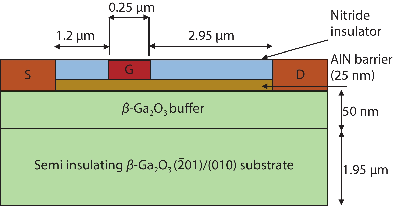
Fig. 1.
(Color online) Schematic cross sectional view of the analysed device structure.
ARTICLES
R. Singh1, T. R. Lenka1, , R. T. Velpula2, B. Jain2, H. Q. T. Bui2 and H. P. T. Nguyen2
Corresponding author: T. R. Lenka, Email: trlenka@ieee.org
Abstract: In this paper, drain current transient characteristics of β-Ga2O3 high electron mobility transistor (HEMT) are studied to access current collapse and recovery time due to dynamic population and de-population of deep level traps and interface traps. An approximately 10 min, and 1 h of recovery time to steady-state drain current value is measured under 1 ms of stress on the gate and drain electrodes due to iron (Fe)–doped β-Ga2O3 substrate and germanium (Ge)–doped β-Ga2O3 epitaxial layer respectively. On-state current lag is more severe due to widely reported defect trap EC – 0.82 eV over EC – 0.78 eV, ?0.75 eV present in Iron (Fe)-doped β-Ga2O3 bulk crystals. A negligible amount of current degradation is observed in the latter case due to the trap level at EC – 0.98 eV. It is found that occupancy of ionized trap density varied mostly under the gate and gate–source area. This investigation of reversible current collapse phenomenon and assessment of recovery time in β-Ga2O3 HEMT is carried out through 2D device simulations using appropriate velocity and charge transport models. This work can further help in the proper characterization of β-Ga2O3 devices to understand temporary and permanent device degradation.
Key words: β-Ga2O3, current collapse, degradation, HEMT, recovery time, traps, trapping effects
| [1] |
He H Y, Orlando R, Blanco M A, et al. First-principles study of the structural, electronic, and optical properties of Ga2O3 in its monoclinic and hexagonal phases. Phys Rev B, 2006, 74, 195123 doi: 10.1103/PhysRevB.74.195123
|
| [2] |
Higashiwaki M, Sasaki K, Kuramata A, et al. Gallium oxide (Ga2O3) metal–semiconductor field-effect transistors on single-crystal β-Ga2O3 (010) substrates. Appl Phys Lett, 2012, 100, 013504 doi: 10.1063/1.3674287
|
| [3] |
Ghosh K, Singisetti U. Ab initio velocity-field curves in monoclinic β-Ga2O3. J Appl Phys, 2017, 122, 035702 doi: 10.1063/1.4986174
|
| [4] |
Varley J B, Weber J R, Janotti A, et al. Oxygen vacancies and donor impurities in β-Ga2O3. Appl Phys Lett, 2010, 97, 142106 doi: 10.1063/1.3499306
|
| [5] |
Chikoidze E, Fellous A, Perez-Tomas A, et al. P-type β-gallium oxide: A new perspective for power and optoelectronic devices. Mater Today Phys, 2017, 3, 118 doi: 10.1016/j.mtphys.2017.10.002
|
| [6] |
Kyrtsos A, Matsubara M, Bellotti E. On the feasibility of p-type Ga2O3. Appl Phys Lett, 2018, 112, 032108 doi: 10.1063/1.5009423
|
| [7] |
Tomm Y, Reiche P, Klimm D, et al. Czochralski grown Ga2O3 crystals. J Cryst Growth, 2000, 220, 510 doi: 10.1016/S0022-0248(00)00851-4
|
| [8] |
Aida H, Nishiguchi K, Takeda H, et al. Growth of β-Ga2O3 single crystals by the edge-defined, film fed growth method. Jpn J Appl Phys, 2008, 47, 8506 doi: 10.1143/JJAP.47.8506
|
| [9] |
Farzana E, Ahmadi E, Speck J S, et al. Deep level defects in Ge-doped (010) β-Ga2O3 layers grown by plasma-assisted molecular beam epitaxy. J Appl Phys, 2018, 123, 161410 doi: 10.1063/1.5010608
|
| [10] |
Zhang Z, Farzana E, Arehart A R, et al. Erratum: “Deep level defects throughout the bandgap of (010) β-Ga2O3 detected by optically and thermally stimulated defect spectroscopy” [Appl. Phys. Lett. 108, 052105 (2016)]. Appl Phys Lett, 2016, 108, 079901 doi: 10.1063/1.4942431
|
| [11] |
Irmscher K, Galazka Z, Pietsch M, et al. Electrical properties of β-Ga2O3 single crystals grown by the Czochralski method. J Appl Phys, 2011, 110, 063720 doi: 10.1063/1.3642962
|
| [12] |
Ingebrigtsen M E, Varley J B, Kuznetsov A Y, et al. Iron and intrinsic deep level states in Ga2O3. Appl Phys Lett, 2018, 112, 042104 doi: 10.1063/1.5020134
|
| [13] |
Sasaki K, Higashiwaki M, Kuramata A, et al. Ga2O3 Schottky barrier diodes fabricated by using single-crystal β-Ga2O3 (010) substrates. IEEE Electron Device Lett, 2013, 34, 493 doi: 10.1109/LED.2013.2244057
|
| [14] |
Krishnamoorthy S, Xia Z B, Bajaj S, et al. Delta-doped β-gallium oxide field-effect transistor. Appl Phys Express, 2017, 10, 051102 doi: 10.7567/APEX.10.051102
|
| [15] |
Zhou H, Maize K, Qiu G, et al. β-Ga2O3 on insulator field-effect transistors with drain currents exceeding 1.5 A/mm and their self-heating effect. Appl Phys Lett, 2017, 111, 092102 doi: 10.1063/1.5000735
|
| [16] |
Oshima T, Kato Y, Kawano N, et al. Carrier confinement observed at modulation-doped β-(Al xGa1– x)2O3/Ga2O3 heterojunction interface. Appl Phys Express, 2017, 10, 035701 doi: 10.7567/APEX.10.035701
|
| [17] |
Zhang Y W, Neal A, Xia Z B, et al. Demonstration of high mobility and quantum transport in modulation-doped β-(Al xGa1 – x)2O3/Ga2O3 heterostructures. Appl Phys Lett, 2018, 112, 173502 doi: 10.1063/1.5025704
|
| [18] |
McGlone J F, Xia Z B, Zhang Y W, et al. Trapping effects in Si δ-doped β-Ga2O3 MESFETs on an Fe-doped β-Ga2O3 substrate. IEEE Electron Device Lett, 2018, 39, 1042 doi: 10.1109/LED.2018.2843344
|
| [19] |
Polyakov A Y, Smirnov N B, Shchemerov I V, et al. Defect states determining dynamic trapping-detrapping in β-Ga2O3 field-effect transistors. ECS J Solid State Sci Technol, 2019, 8, Q3013 doi: 10.1149/2.0031907jss
|
| [20] |
Sun H D, Torres Castanedo C G, Liu K K, et al. Valence and conduction band offsets of β-Ga2O3/AlN heterojunction. Appl Phys Lett, 2017, 111, 162105 doi: 10.1063/1.5003930
|
| [21] |
Mock A, Korlacki R, Briley C, et al. Band-to-band transitions, selection rules, effective mass, and excitonic contributions in monoclinic β-Ga2O3. Phys Rev B, 2017, 96, 245205 doi: 10.1103/PhysRevB.96.245205
|
| [22] |
Device simulation software, ATLAS user’s manual. Silvaco, Santa Clara, CA, USA, 2009
|
| [23] |
Lu Y, Yao H H, Li J, et al. AlN/β-Ga2O3 based HEMT: A potential pathway to ultimate high power device. arXiv: 1901.05111, 2019
|
| [24] |
Balaz D. Current collapse and device degradation in AlGaN/GaN heterostructure field effect transistors. Ph D Dissertation, University of Glasgow, 2011
|
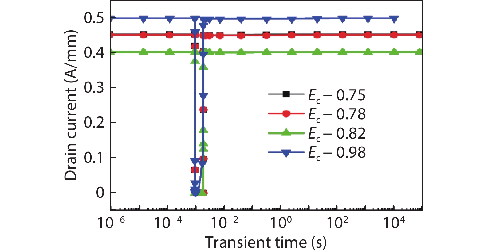
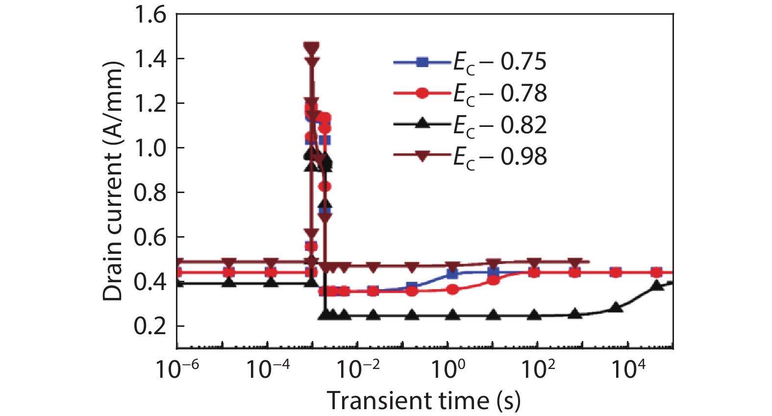
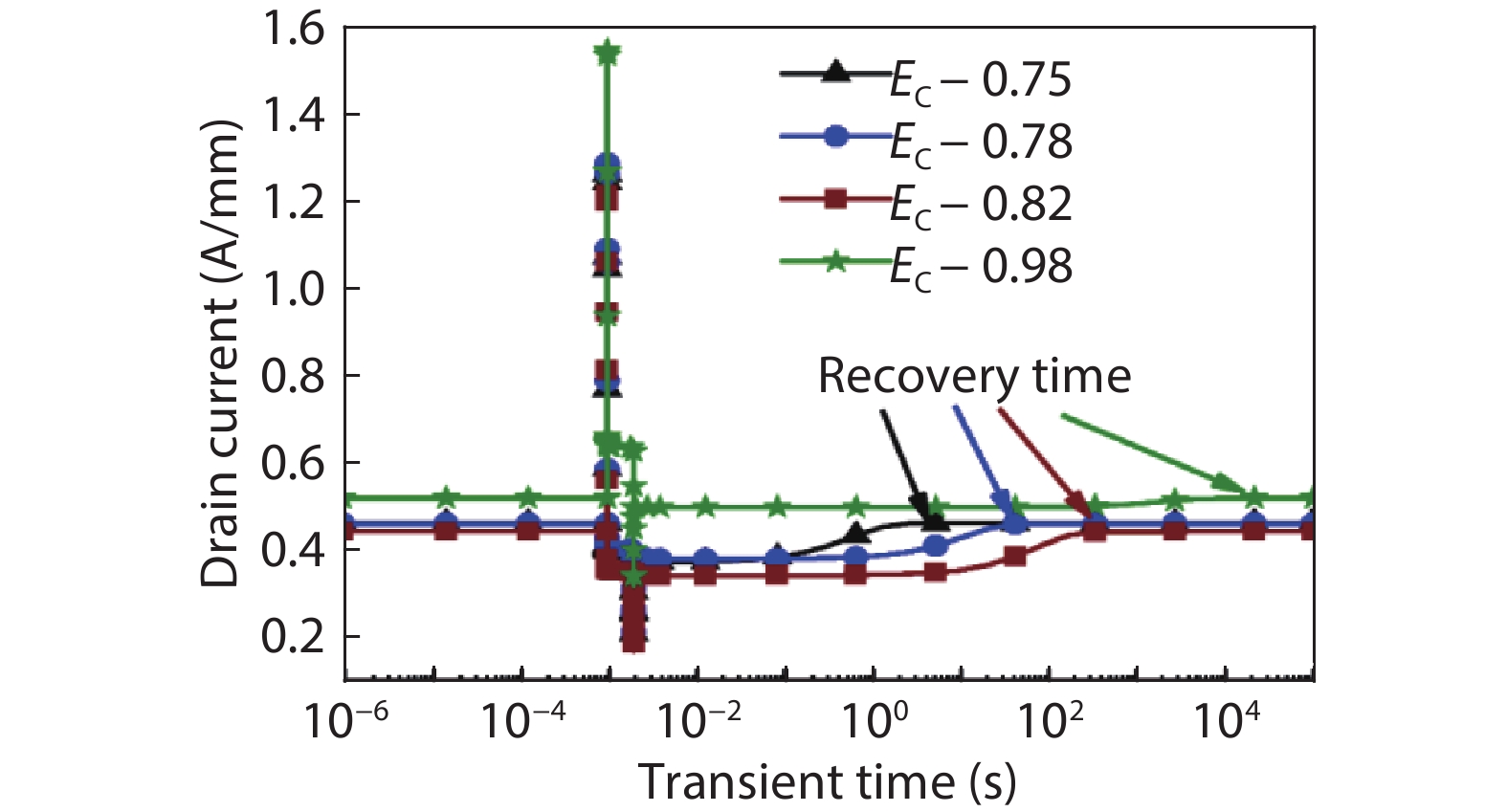
Table 1. Deep level traps reported in β-Ga2O3 substrate and epitaxial layer, energy level, capture cross section and trap concentration. Fe and Ge enabled current collapse and drain current recovery time to pre-stress condition.
| Reference | Trap energy levels (eV) | Capture cross section (10?14 cm–2) | Trap source | Trap concentration (1015 cm–3) | Current collapse/ recovery time |
| [12] | EC – 0.78 | 0.7 | Fe-doped substrate ( | 10 | Moderate/ few seconds |
| EC – 0.75 | 5 | Fe-doped substrate ( | 10 | Moderate/ few minutes | |
| [9] | EC – 0.98 | 0.1? 9 | Ge-doped PAMBE on (010) substrate | 1.6 | Mild/ ~ 1 h |
| [10] | EC – 0.82 | 1 | UID bulk EFG wafer (010) | 36 | Severe/ ~ 10 min |
 DownLoad: CSV
| [1] |
He H Y, Orlando R, Blanco M A, et al. First-principles study of the structural, electronic, and optical properties of Ga2O3 in its monoclinic and hexagonal phases. Phys Rev B, 2006, 74, 195123 doi: 10.1103/PhysRevB.74.195123
|
| [2] |
Higashiwaki M, Sasaki K, Kuramata A, et al. Gallium oxide (Ga2O3) metal–semiconductor field-effect transistors on single-crystal β-Ga2O3 (010) substrates. Appl Phys Lett, 2012, 100, 013504 doi: 10.1063/1.3674287
|
| [3] |
Ghosh K, Singisetti U. Ab initio velocity-field curves in monoclinic β-Ga2O3. J Appl Phys, 2017, 122, 035702 doi: 10.1063/1.4986174
|
| [4] |
Varley J B, Weber J R, Janotti A, et al. Oxygen vacancies and donor impurities in β-Ga2O3. Appl Phys Lett, 2010, 97, 142106 doi: 10.1063/1.3499306
|
| [5] |
Chikoidze E, Fellous A, Perez-Tomas A, et al. P-type β-gallium oxide: A new perspective for power and optoelectronic devices. Mater Today Phys, 2017, 3, 118 doi: 10.1016/j.mtphys.2017.10.002
|
| [6] |
Kyrtsos A, Matsubara M, Bellotti E. On the feasibility of p-type Ga2O3. Appl Phys Lett, 2018, 112, 032108 doi: 10.1063/1.5009423
|
| [7] |
Tomm Y, Reiche P, Klimm D, et al. Czochralski grown Ga2O3 crystals. J Cryst Growth, 2000, 220, 510 doi: 10.1016/S0022-0248(00)00851-4
|
| [8] |
Aida H, Nishiguchi K, Takeda H, et al. Growth of β-Ga2O3 single crystals by the edge-defined, film fed growth method. Jpn J Appl Phys, 2008, 47, 8506 doi: 10.1143/JJAP.47.8506
|
| [9] |
Farzana E, Ahmadi E, Speck J S, et al. Deep level defects in Ge-doped (010) β-Ga2O3 layers grown by plasma-assisted molecular beam epitaxy. J Appl Phys, 2018, 123, 161410 doi: 10.1063/1.5010608
|
| [10] |
Zhang Z, Farzana E, Arehart A R, et al. Erratum: “Deep level defects throughout the bandgap of (010) β-Ga2O3 detected by optically and thermally stimulated defect spectroscopy” [Appl. Phys. Lett. 108, 052105 (2016)]. Appl Phys Lett, 2016, 108, 079901 doi: 10.1063/1.4942431
|
| [11] |
Irmscher K, Galazka Z, Pietsch M, et al. Electrical properties of β-Ga2O3 single crystals grown by the Czochralski method. J Appl Phys, 2011, 110, 063720 doi: 10.1063/1.3642962
|
| [12] |
Ingebrigtsen M E, Varley J B, Kuznetsov A Y, et al. Iron and intrinsic deep level states in Ga2O3. Appl Phys Lett, 2018, 112, 042104 doi: 10.1063/1.5020134
|
| [13] |
Sasaki K, Higashiwaki M, Kuramata A, et al. Ga2O3 Schottky barrier diodes fabricated by using single-crystal β-Ga2O3 (010) substrates. IEEE Electron Device Lett, 2013, 34, 493 doi: 10.1109/LED.2013.2244057
|
| [14] |
Krishnamoorthy S, Xia Z B, Bajaj S, et al. Delta-doped β-gallium oxide field-effect transistor. Appl Phys Express, 2017, 10, 051102 doi: 10.7567/APEX.10.051102
|
| [15] |
Zhou H, Maize K, Qiu G, et al. β-Ga2O3 on insulator field-effect transistors with drain currents exceeding 1.5 A/mm and their self-heating effect. Appl Phys Lett, 2017, 111, 092102 doi: 10.1063/1.5000735
|
| [16] |
Oshima T, Kato Y, Kawano N, et al. Carrier confinement observed at modulation-doped β-(Al xGa1– x)2O3/Ga2O3 heterojunction interface. Appl Phys Express, 2017, 10, 035701 doi: 10.7567/APEX.10.035701
|
| [17] |
Zhang Y W, Neal A, Xia Z B, et al. Demonstration of high mobility and quantum transport in modulation-doped β-(Al xGa1 – x)2O3/Ga2O3 heterostructures. Appl Phys Lett, 2018, 112, 173502 doi: 10.1063/1.5025704
|
| [18] |
McGlone J F, Xia Z B, Zhang Y W, et al. Trapping effects in Si δ-doped β-Ga2O3 MESFETs on an Fe-doped β-Ga2O3 substrate. IEEE Electron Device Lett, 2018, 39, 1042 doi: 10.1109/LED.2018.2843344
|
| [19] |
Polyakov A Y, Smirnov N B, Shchemerov I V, et al. Defect states determining dynamic trapping-detrapping in β-Ga2O3 field-effect transistors. ECS J Solid State Sci Technol, 2019, 8, Q3013 doi: 10.1149/2.0031907jss
|
| [20] |
Sun H D, Torres Castanedo C G, Liu K K, et al. Valence and conduction band offsets of β-Ga2O3/AlN heterojunction. Appl Phys Lett, 2017, 111, 162105 doi: 10.1063/1.5003930
|
| [21] |
Mock A, Korlacki R, Briley C, et al. Band-to-band transitions, selection rules, effective mass, and excitonic contributions in monoclinic β-Ga2O3. Phys Rev B, 2017, 96, 245205 doi: 10.1103/PhysRevB.96.245205
|
| [22] |
Device simulation software, ATLAS user’s manual. Silvaco, Santa Clara, CA, USA, 2009
|
| [23] |
Lu Y, Yao H H, Li J, et al. AlN/β-Ga2O3 based HEMT: A potential pathway to ultimate high power device. arXiv: 1901.05111, 2019
|
| [24] |
Balaz D. Current collapse and device degradation in AlGaN/GaN heterostructure field effect transistors. Ph D Dissertation, University of Glasgow, 2011
|


Article views: 5288 Times PDF downloads: 121 Times Cited by: 0 Times
Received: 12 February 2020 Revised: 27 May 2020 Online: Accepted Manuscript: 28 June 2020Uncorrected proof: 01 July 2020Published: 01 October 2020
| Citation: |
R. Singh, T. R. Lenka, R. T. Velpula, B. Jain, H. Q. T. Bui, H. P. T. Nguyen. Investigation of current collapse and recovery time due to deep level defect traps in β-Ga2O3 HEMT[J]. Journal of Semiconductors, 2020, 41(10): 102802. doi: 10.1088/1674-4926/41/10/102802
****
R Singh, T R Lenka, R T Velpula, B Jain, H Q T Bui, H P T Nguyen, Investigation of current collapse and recovery time due to deep level defect traps in β-Ga2O3 HEMT[J]. J. Semicond., 2020, 41(10): 102802. doi: 10.1088/1674-4926/41/10/102802.

|
| [1] |
He H Y, Orlando R, Blanco M A, et al. First-principles study of the structural, electronic, and optical properties of Ga2O3 in its monoclinic and hexagonal phases. Phys Rev B, 2006, 74, 195123 doi: 10.1103/PhysRevB.74.195123
|
| [2] |
Higashiwaki M, Sasaki K, Kuramata A, et al. Gallium oxide (Ga2O3) metal–semiconductor field-effect transistors on single-crystal β-Ga2O3 (010) substrates. Appl Phys Lett, 2012, 100, 013504 doi: 10.1063/1.3674287
|
| [3] |
Ghosh K, Singisetti U. Ab initio velocity-field curves in monoclinic β-Ga2O3. J Appl Phys, 2017, 122, 035702 doi: 10.1063/1.4986174
|
| [4] |
Varley J B, Weber J R, Janotti A, et al. Oxygen vacancies and donor impurities in β-Ga2O3. Appl Phys Lett, 2010, 97, 142106 doi: 10.1063/1.3499306
|
| [5] |
Chikoidze E, Fellous A, Perez-Tomas A, et al. P-type β-gallium oxide: A new perspective for power and optoelectronic devices. Mater Today Phys, 2017, 3, 118 doi: 10.1016/j.mtphys.2017.10.002
|
| [6] |
Kyrtsos A, Matsubara M, Bellotti E. On the feasibility of p-type Ga2O3. Appl Phys Lett, 2018, 112, 032108 doi: 10.1063/1.5009423
|
| [7] |
Tomm Y, Reiche P, Klimm D, et al. Czochralski grown Ga2O3 crystals. J Cryst Growth, 2000, 220, 510 doi: 10.1016/S0022-0248(00)00851-4
|
| [8] |
Aida H, Nishiguchi K, Takeda H, et al. Growth of β-Ga2O3 single crystals by the edge-defined, film fed growth method. Jpn J Appl Phys, 2008, 47, 8506 doi: 10.1143/JJAP.47.8506
|
| [9] |
Farzana E, Ahmadi E, Speck J S, et al. Deep level defects in Ge-doped (010) β-Ga2O3 layers grown by plasma-assisted molecular beam epitaxy. J Appl Phys, 2018, 123, 161410 doi: 10.1063/1.5010608
|
| [10] |
Zhang Z, Farzana E, Arehart A R, et al. Erratum: “Deep level defects throughout the bandgap of (010) β-Ga2O3 detected by optically and thermally stimulated defect spectroscopy” [Appl. Phys. Lett. 108, 052105 (2016)]. Appl Phys Lett, 2016, 108, 079901 doi: 10.1063/1.4942431
|
| [11] |
Irmscher K, Galazka Z, Pietsch M, et al. Electrical properties of β-Ga2O3 single crystals grown by the Czochralski method. J Appl Phys, 2011, 110, 063720 doi: 10.1063/1.3642962
|
| [12] |
Ingebrigtsen M E, Varley J B, Kuznetsov A Y, et al. Iron and intrinsic deep level states in Ga2O3. Appl Phys Lett, 2018, 112, 042104 doi: 10.1063/1.5020134
|
| [13] |
Sasaki K, Higashiwaki M, Kuramata A, et al. Ga2O3 Schottky barrier diodes fabricated by using single-crystal β-Ga2O3 (010) substrates. IEEE Electron Device Lett, 2013, 34, 493 doi: 10.1109/LED.2013.2244057
|
| [14] |
Krishnamoorthy S, Xia Z B, Bajaj S, et al. Delta-doped β-gallium oxide field-effect transistor. Appl Phys Express, 2017, 10, 051102 doi: 10.7567/APEX.10.051102
|
| [15] |
Zhou H, Maize K, Qiu G, et al. β-Ga2O3 on insulator field-effect transistors with drain currents exceeding 1.5 A/mm and their self-heating effect. Appl Phys Lett, 2017, 111, 092102 doi: 10.1063/1.5000735
|
| [16] |
Oshima T, Kato Y, Kawano N, et al. Carrier confinement observed at modulation-doped β-(Al xGa1– x)2O3/Ga2O3 heterojunction interface. Appl Phys Express, 2017, 10, 035701 doi: 10.7567/APEX.10.035701
|
| [17] |
Zhang Y W, Neal A, Xia Z B, et al. Demonstration of high mobility and quantum transport in modulation-doped β-(Al xGa1 – x)2O3/Ga2O3 heterostructures. Appl Phys Lett, 2018, 112, 173502 doi: 10.1063/1.5025704
|
| [18] |
McGlone J F, Xia Z B, Zhang Y W, et al. Trapping effects in Si δ-doped β-Ga2O3 MESFETs on an Fe-doped β-Ga2O3 substrate. IEEE Electron Device Lett, 2018, 39, 1042 doi: 10.1109/LED.2018.2843344
|
| [19] |
Polyakov A Y, Smirnov N B, Shchemerov I V, et al. Defect states determining dynamic trapping-detrapping in β-Ga2O3 field-effect transistors. ECS J Solid State Sci Technol, 2019, 8, Q3013 doi: 10.1149/2.0031907jss
|
| [20] |
Sun H D, Torres Castanedo C G, Liu K K, et al. Valence and conduction band offsets of β-Ga2O3/AlN heterojunction. Appl Phys Lett, 2017, 111, 162105 doi: 10.1063/1.5003930
|
| [21] |
Mock A, Korlacki R, Briley C, et al. Band-to-band transitions, selection rules, effective mass, and excitonic contributions in monoclinic β-Ga2O3. Phys Rev B, 2017, 96, 245205 doi: 10.1103/PhysRevB.96.245205
|
| [22] |
Device simulation software, ATLAS user’s manual. Silvaco, Santa Clara, CA, USA, 2009
|
| [23] |
Lu Y, Yao H H, Li J, et al. AlN/β-Ga2O3 based HEMT: A potential pathway to ultimate high power device. arXiv: 1901.05111, 2019
|
| [24] |
Balaz D. Current collapse and device degradation in AlGaN/GaN heterostructure field effect transistors. Ph D Dissertation, University of Glasgow, 2011
|

 WeChat ID
Journal of Semiconductors © 2017 All Rights Reserved 京ICP備05085259號(hào)-2

