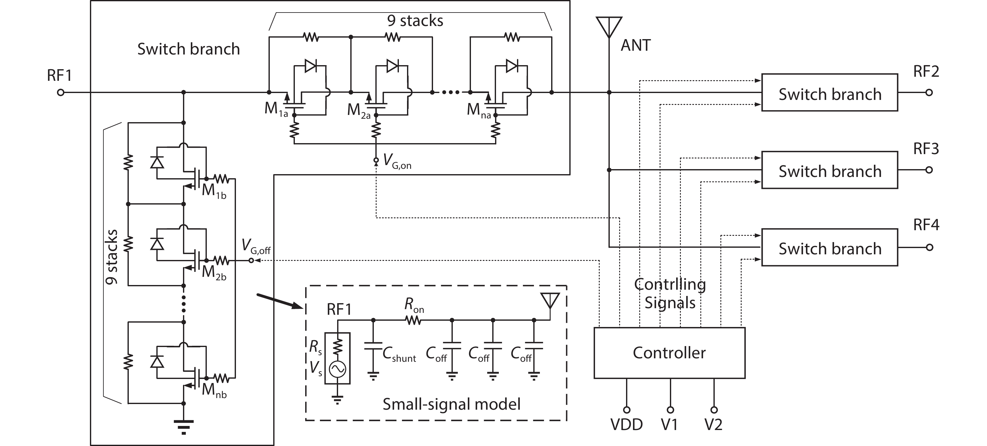
Fig. 1.
The block diagram of the proposed SP4T switch. Schematic of a single switch branch is depicted.
ARTICLES
Hao Zhang1, *, Qiangsheng Cui2, *, Xu Yan1, 3, Jiahui Shi1 and Fujiang Lin1,
Corresponding author: F J Lin, linfj@ustc.edu.cn
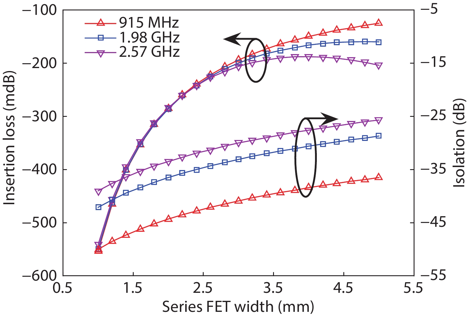
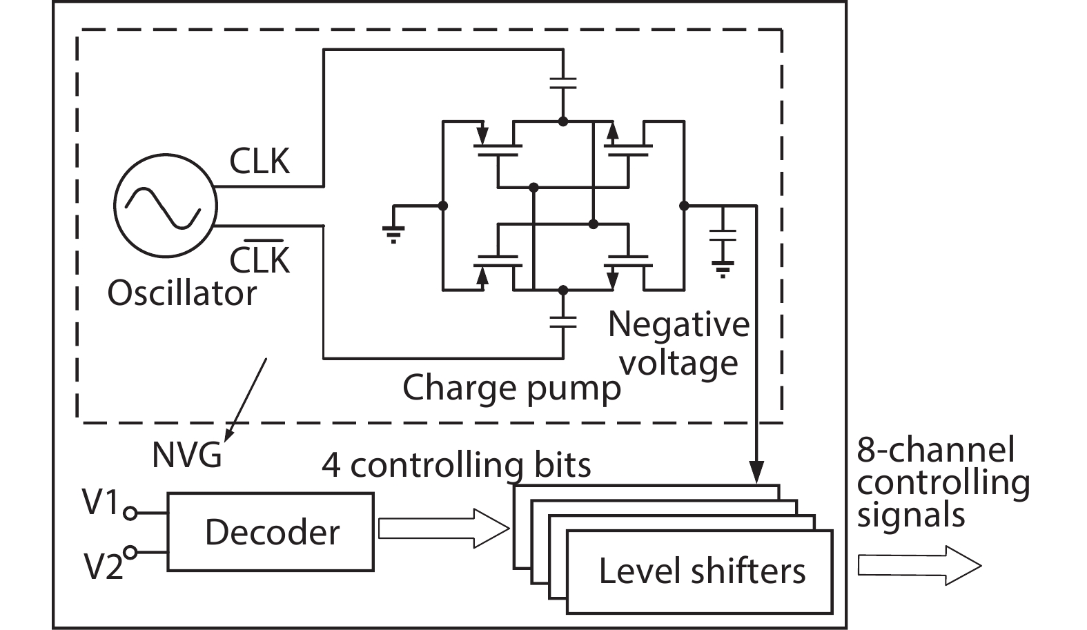
Abstract: A single-pole four-throw (SP4T) RF switch with charge-pump-based controller is designed and implemented in a commercial 130-nm silicon-on-insulator (SOI) CMOS process. An improved body self-biasing technique based on diodes is utilized to simplify the controlling circuitry and improve the linearity. A multistack field-effect-transistor (FET) structure with body floating technique is employed to provide good power-handling capability. The proposed design demonstrates a measured input 0.1-dB compression point of 38.5 dBm at 1.9 GHz, an insertion loss of 0.27 dB/0.33 dB and an isolation of 35 dB/27 dB at 900 MHz/1.9 GHz, respectively. The overall chip area is only 0.49 mm2. This RF switch can be used in GSM/WCDMA/LTE front-end modules.
Key words: RF switch, silicon-on-insulator, body self-biasing technique, multistack FETs
| [1] |
Yan X, Li Y, Chen Y, et al. A LNA-merged RF front-end with digitally assisted technique for gain flatness and input-match compensation. Analog Integr Circuits Signal Process, 2019, 101, 219 doi: 10.1007/s10470-019-01539-2
|
| [2] |
Zhang H, Yan X, Shi J H, et al. A 0.5–5.6 GHz inductorless wideband LNA with local active feedback. 2018 IEEE 3rd International Conference on Integrated Circuits and Microsystems (ICICM), 2018, 164
|
| [3] |
Yan X, Chen C, Yang L, et al. A 0.1–1.1 GHz inductorless differential LNA with double gm -boosting and positive feedback. Analog Integr Circuits Signal Process, 2017, 93, 205 doi: 10.1007/s10470-017-1043-y
|
| [4] |
Huang C W P, Christainsen K, Nabokin S, et al. A highly integrated single chip 5–6 GHz front-end IC based on SiGe BiCMOS that enhances 802.11ac WLAN radio front-end designs. 2015 IEEE Radio Freq Integr Circuits Symp RFIC, 2015, 227
|
| [5] |
Im D, Kim B K, Im D K, et al. A stacked-FET linear SOI CMOS cellular antenna switch with an extremely low-power biasing strategy. IEEE Trans Microw Theory Tech, 2015, 63, 1964 doi: 10.1109/TMTT.2015.2427801
|
| [6] |
Ahn M, Cha J, Cho C, et al. Ultra low loss and high linearity SPMT antenna switch using SOI CMOS process. 40th Eur Microw Conf, 2010, 652
|
| [7] |
Joshi A B, Lee S, Chen Y Y, et al. Optimized CMOS-SOI process for high performance RF switches. 2012 IEEE Int SOI Conf SOI, 2012, 1
|
| [8] |
Ben Ali K, Roda Neve C, Gharsallah A, et al. Ultrawide frequency range crosstalk into standard and trap-rich high resistivity silicon substrates. IEEE Trans Electron Devices, 2011, 58, 4258 doi: 10.1109/TED.2011.2170074
|
| [9] |
Wang X S, Yue C P. A dual-band SP6T t/r switch in SOI CMOS with 37-dBm P–0.1 dB for GSM/W-CDMA handsets. IEEE Trans Theory Technol, 2014, 62, 861 doi: 10.1109/TMTT.2014.2308306
|
| [10] |
Ohnakado T, Yamakawa S, Murakami T, et al. 21.5 dBm power-handling 5 GHz transmit/receive CMOS switch realized by voltage division effect of stacked transistor configuration with depletion-layer-extended transistors (DETs). 2003 Symp VLSI Circuits Dig Tech Pap, 2003, 1152, 25
|
| [11] |
Ahn M, Lee C H, Kim B S, et al. A high-power CMOS switch using A novel adaptive voltage swing distribution method in multistack FETs. IEEE Trans Microw Theory Tech, 2008, 56, 849 doi: 10.1109/TMTT.2008.919047
|
| [12] |
Ahn M, Kim H W, Lee C H, et al. A 1.8-GHz 33-dBm P0.1-dB CMOS T/R switch using stacked FETs with feed-forward capacitors in a floated well structure. IEEE Trans Microw Theory Tech, 2009, 57, 2661 doi: 10.1109/TMTT.2009.2031928
|
| [13] |
Cui J, Chen L, Liu Y. Monolithic single-pole sixteen-throw T/R switch for next-generation front-end module. IEEE Microw Wirel Compon Lett, 2014, 24, 345 doi: 10.1109/LMWC.2014.2309082
|
| [14] |
Yeh M C, Tsai Z M, Liu R C, et al. Design and analysis for a miniature CMOS SPDT switch using body-floating technique to improve power performance. IEEE Trans Microw Theory Tech, 2006, 54, 31 doi: 10.1109/TMTT.2005.860894
|
| [15] |
Tinella C, Richard O, Cathelin A, et al. 0.13 μm CMOS SOI SP6T antenna switch for multi-standard handsets. 2006 Topical Meeting on Silicon Monolithic Integrated Circuits in RF Systems, 2006, 4
|
| [16] |
Zhang Z H, Huang L, Yu K, et al. A novel body self-biased technique for enhanced RF performance of a SP8T antenna switch in partially depleted CMOS-SOI technology. 2014 12th IEEE International Conference on Solid-State and Integrated Circuit Technology (ICSICT), 2014, 1
|
| [17] |
Xu H F, Kenneth K O. A 31.3-dBm bulk CMOS T/R switch using stacked transistors with sub-design-rule channel length in floated p-wells. IEEE J Solid-State Circuits, 2007, 42, 2528 doi: 10.1109/JSSC.2007.907201
|
| [18] |
Tseng Y C, Huang W M, Monk D J, et al. AC floating body effects and the resultant analog circuit issues in submicron floating body and body-grounded SOI MOSFET's. IEEE Trans Electron Devices, 1999, 46, 1685 doi: 10.1109/16.777157
|
| [19] |
Cha J, Ahn M, Cho C, et al. Analysis and design techniques of CMOS charge-pump-based radio-frequency antenna-switch controllers. IEEE Trans Circuits Syst I, 2009, 56, 1053 doi: 10.1109/TCSI.2009.2016129
|
| [20] |
Zhu H W, Li Q L, Sun H, et al. Ultra low loss and high linearity RF switch using 130 nm SOI CMOS process. 2017 IEEE 12th International Conference on ASIC (ASICON), 2017, 698
|
| [21] |
Guan H, Sun H, Bao J L, et al. High-performance RF switch in 0.13 μm RF SOI process. J Semicond, 2019, 40, 022401 doi: 10.1088/1674-4926/40/2/022401
|
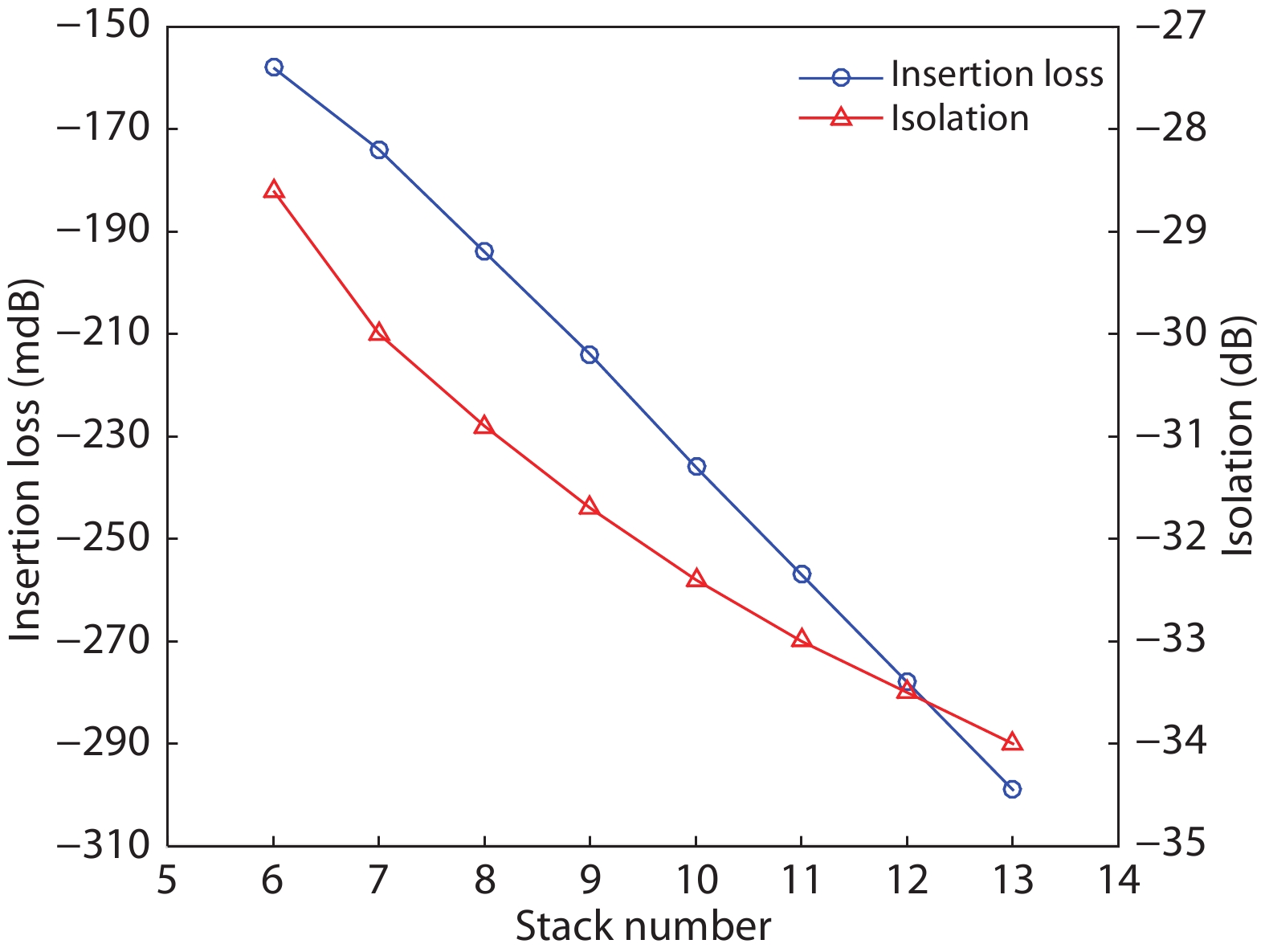
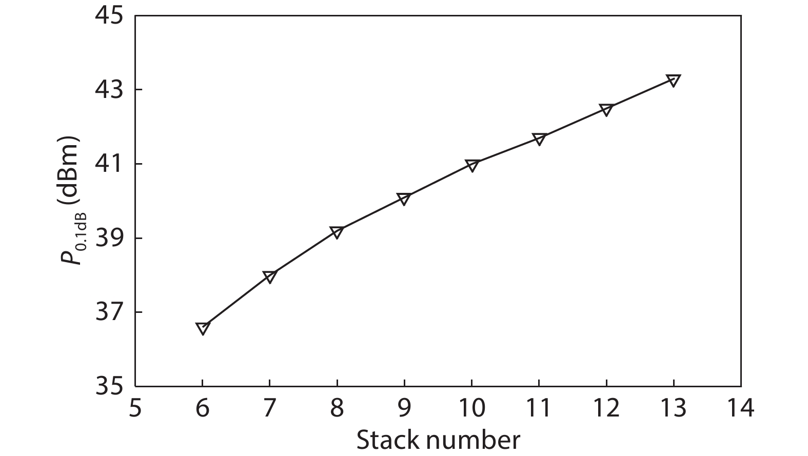
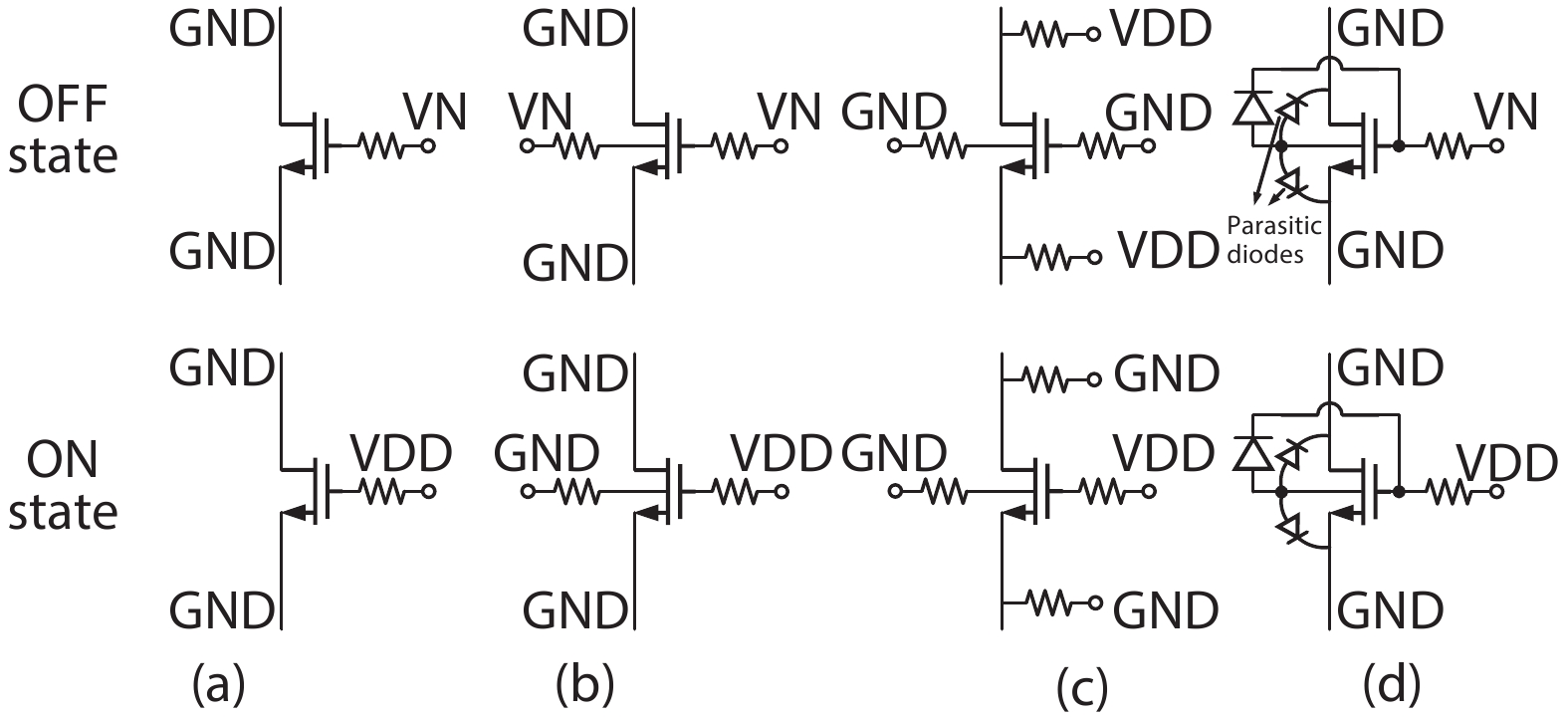
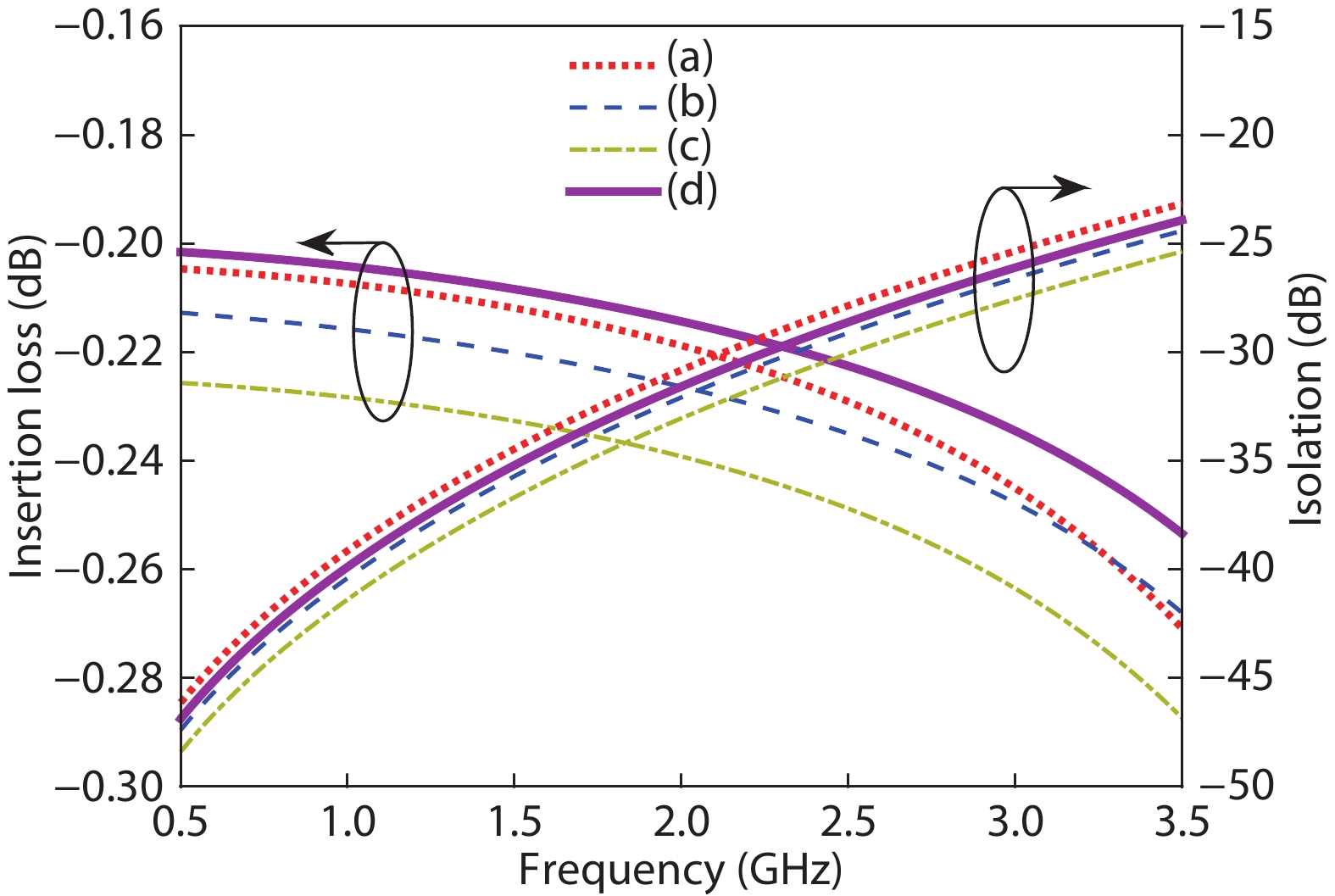
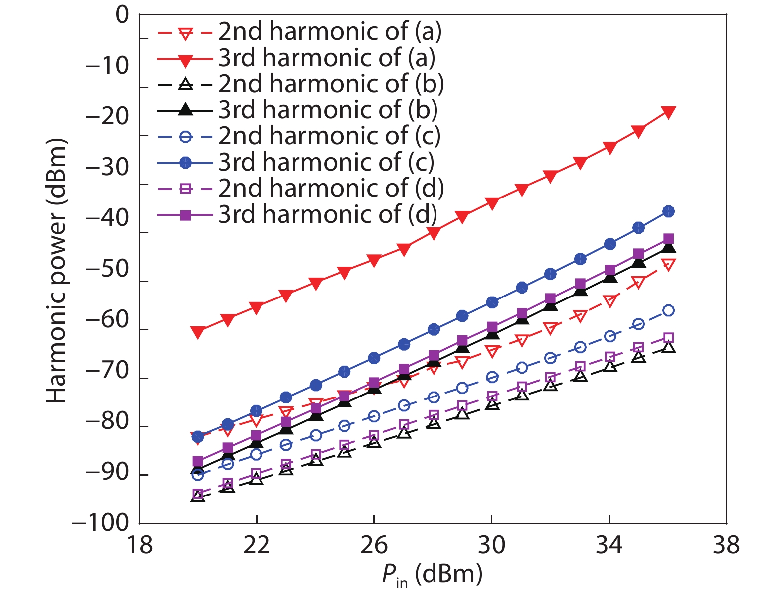
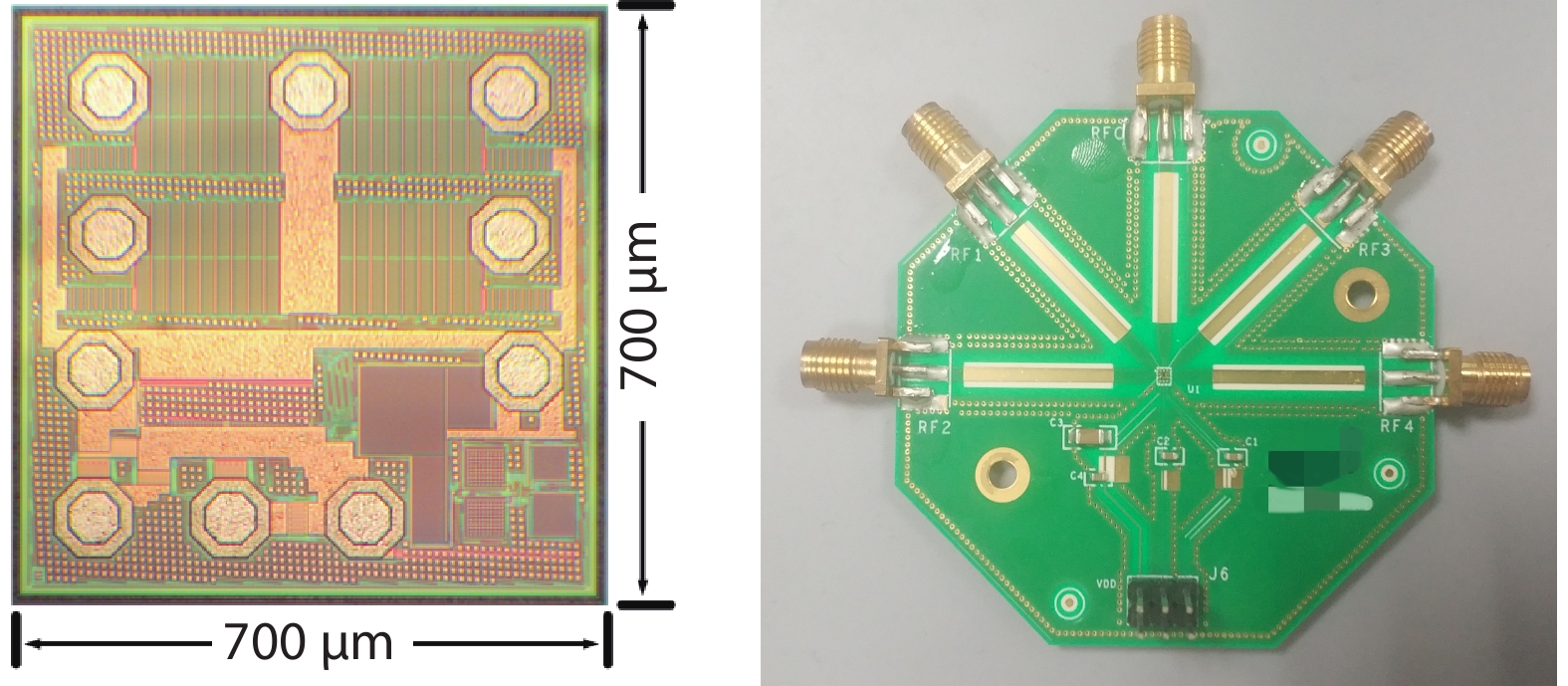
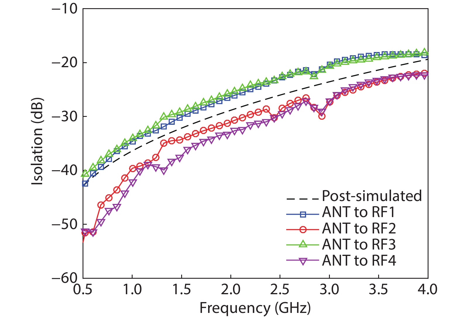
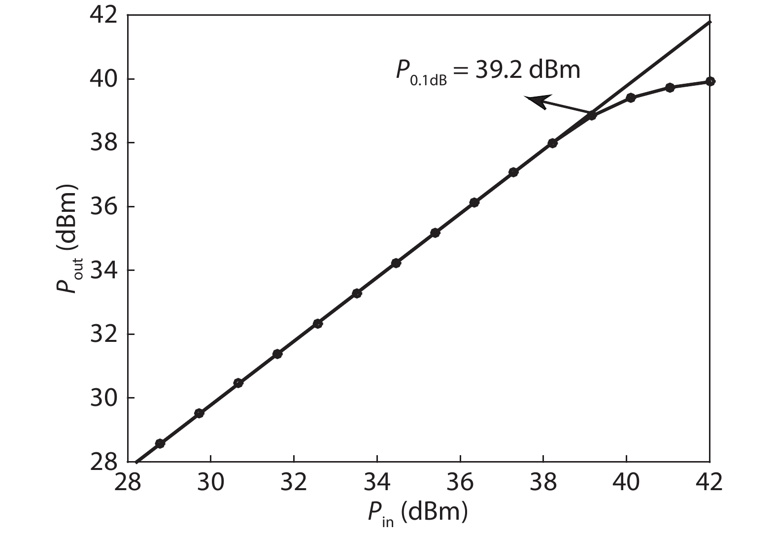
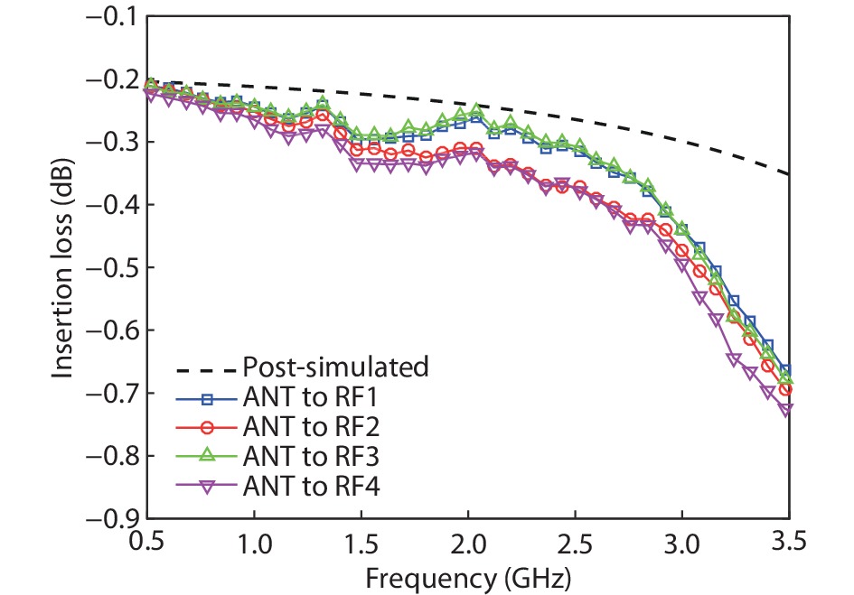
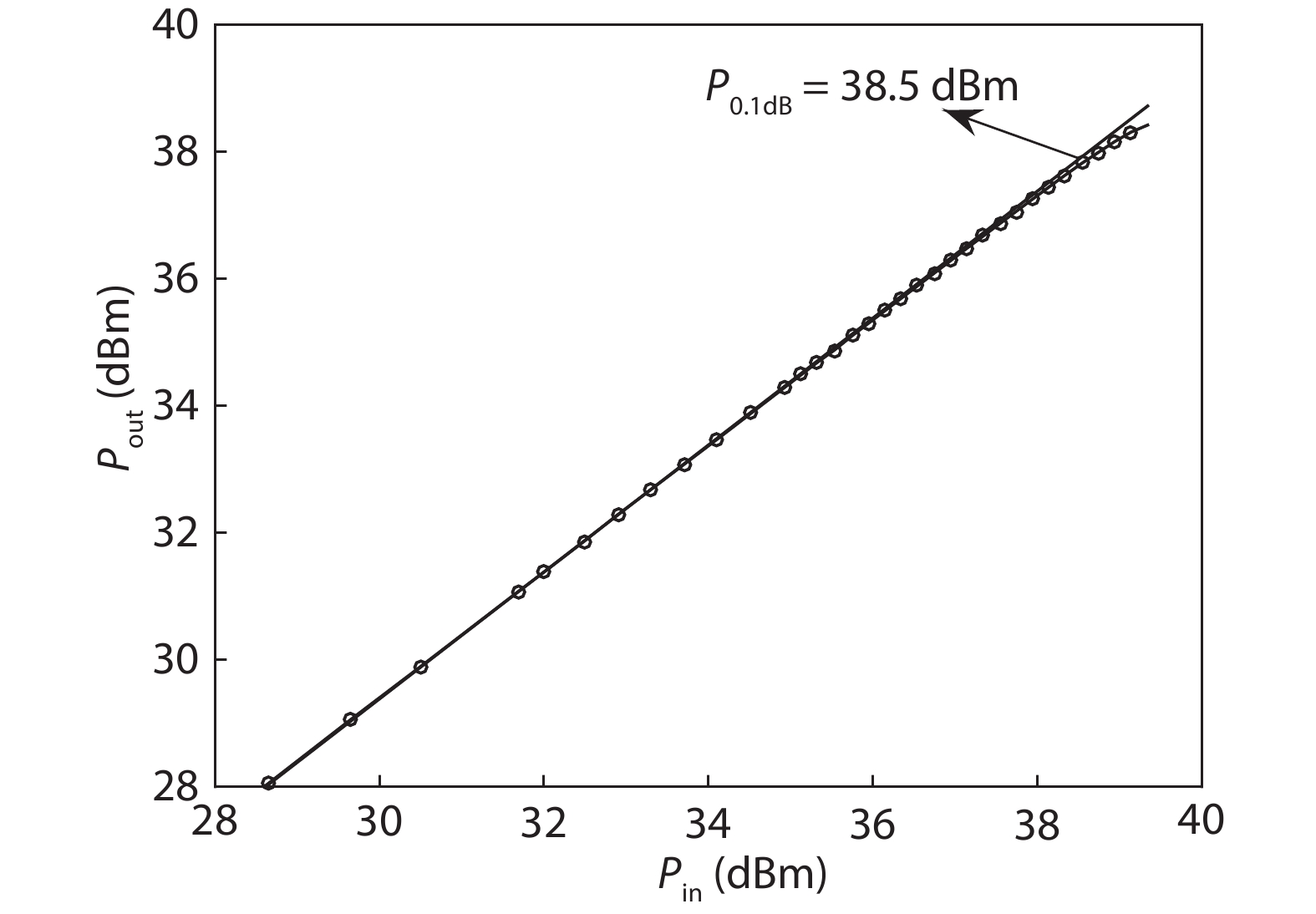
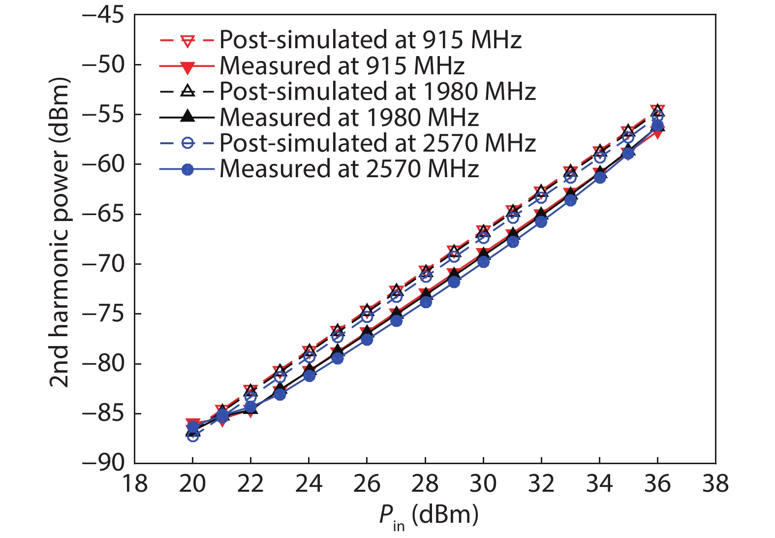
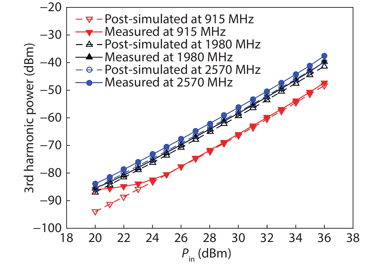
Table 1. P0.1 dB at 1.9 GHz of different biasing strategies.
| Biasing | (a) | (b) | (c) | (d) |
| P0.1 dB (dBm) | 37.3 | 40.2 | 36.7 | 40.1 |
 DownLoad: CSV
Table 2. Comparison of RF switch performance.
| Parameter | Ref. [5] | Ref. [6] | Ref. [20] | Ref. [21] | This work |
| SPXT | SP4T | SP4T | SPDT | SPST | SP4T |
| f (GHz) | 0.90/1.9 | 0.90/1.9 | 0.90/1.9 | 0.90/1.9 | 0.90/1.9 |
| Insertion loss (dB) | 0.49/0.70 | 0.30/0.37 | 0.25/0.30 | 0.24/0.34 | 0.27/0.33 |
| Isolation (dB) | 37/32 | 40/33 | 29/22 | 29/22 | 35/27 |
| P0.1 dB (dBm) | 38* | NA | 35* | 36 | 38.5 |
| 2nd Harmonic (dBc)** | 82/83 | 90/83 | 91/NA | 96**** | 91/96 |
| 3rd Harmonic (dBc)** | 80/81 | 85/78 | 88/NA | 78**** | 82/83 |
| Area (mm2) | 0.98*** | 1.01*** | 0.43 | 0.20 | 0.49*** |
| Stack number | 10 | NA | 10 | 10 | 9 |
| Biasing strategy | Improved dc-lifting | RBFT | RBFT | pFET body self-biasing | Diode body self-biasing |
| Technology | 0.25 μm SOI CMOS | 0.13 μm SOI CMOS | 0.13 μm SOI CMOS | 0.13 μm SOI CMOS | 0.13 μm SOI CMOS |
| * 1-dB compression point. **Pin = 35 dBm at 900 MHz and 33 dBm at 1.9 GHz. *** including controller. **** frequency not specified. | |||||
DownLoad: CSV
| [1] |
Yan X, Li Y, Chen Y, et al. A LNA-merged RF front-end with digitally assisted technique for gain flatness and input-match compensation. Analog Integr Circuits Signal Process, 2019, 101, 219 doi: 10.1007/s10470-019-01539-2
|
| [2] |
Zhang H, Yan X, Shi J H, et al. A 0.5–5.6 GHz inductorless wideband LNA with local active feedback. 2018 IEEE 3rd International Conference on Integrated Circuits and Microsystems (ICICM), 2018, 164
|
| [3] |
Yan X, Chen C, Yang L, et al. A 0.1–1.1 GHz inductorless differential LNA with double gm -boosting and positive feedback. Analog Integr Circuits Signal Process, 2017, 93, 205 doi: 10.1007/s10470-017-1043-y
|
| [4] |
Huang C W P, Christainsen K, Nabokin S, et al. A highly integrated single chip 5–6 GHz front-end IC based on SiGe BiCMOS that enhances 802.11ac WLAN radio front-end designs. 2015 IEEE Radio Freq Integr Circuits Symp RFIC, 2015, 227
|
| [5] |
Im D, Kim B K, Im D K, et al. A stacked-FET linear SOI CMOS cellular antenna switch with an extremely low-power biasing strategy. IEEE Trans Microw Theory Tech, 2015, 63, 1964 doi: 10.1109/TMTT.2015.2427801
|
| [6] |
Ahn M, Cha J, Cho C, et al. Ultra low loss and high linearity SPMT antenna switch using SOI CMOS process. 40th Eur Microw Conf, 2010, 652
|
| [7] |
Joshi A B, Lee S, Chen Y Y, et al. Optimized CMOS-SOI process for high performance RF switches. 2012 IEEE Int SOI Conf SOI, 2012, 1
|
| [8] |
Ben Ali K, Roda Neve C, Gharsallah A, et al. Ultrawide frequency range crosstalk into standard and trap-rich high resistivity silicon substrates. IEEE Trans Electron Devices, 2011, 58, 4258 doi: 10.1109/TED.2011.2170074
|
| [9] |
Wang X S, Yue C P. A dual-band SP6T t/r switch in SOI CMOS with 37-dBm P–0.1 dB for GSM/W-CDMA handsets. IEEE Trans Theory Technol, 2014, 62, 861 doi: 10.1109/TMTT.2014.2308306
|
| [10] |
Ohnakado T, Yamakawa S, Murakami T, et al. 21.5 dBm power-handling 5 GHz transmit/receive CMOS switch realized by voltage division effect of stacked transistor configuration with depletion-layer-extended transistors (DETs). 2003 Symp VLSI Circuits Dig Tech Pap, 2003, 1152, 25
|
| [11] |
Ahn M, Lee C H, Kim B S, et al. A high-power CMOS switch using A novel adaptive voltage swing distribution method in multistack FETs. IEEE Trans Microw Theory Tech, 2008, 56, 849 doi: 10.1109/TMTT.2008.919047
|
| [12] |
Ahn M, Kim H W, Lee C H, et al. A 1.8-GHz 33-dBm P0.1-dB CMOS T/R switch using stacked FETs with feed-forward capacitors in a floated well structure. IEEE Trans Microw Theory Tech, 2009, 57, 2661 doi: 10.1109/TMTT.2009.2031928
|
| [13] |
Cui J, Chen L, Liu Y. Monolithic single-pole sixteen-throw T/R switch for next-generation front-end module. IEEE Microw Wirel Compon Lett, 2014, 24, 345 doi: 10.1109/LMWC.2014.2309082
|
| [14] |
Yeh M C, Tsai Z M, Liu R C, et al. Design and analysis for a miniature CMOS SPDT switch using body-floating technique to improve power performance. IEEE Trans Microw Theory Tech, 2006, 54, 31 doi: 10.1109/TMTT.2005.860894
|
| [15] |
Tinella C, Richard O, Cathelin A, et al. 0.13 μm CMOS SOI SP6T antenna switch for multi-standard handsets. 2006 Topical Meeting on Silicon Monolithic Integrated Circuits in RF Systems, 2006, 4
|
| [16] |
Zhang Z H, Huang L, Yu K, et al. A novel body self-biased technique for enhanced RF performance of a SP8T antenna switch in partially depleted CMOS-SOI technology. 2014 12th IEEE International Conference on Solid-State and Integrated Circuit Technology (ICSICT), 2014, 1
|
| [17] |
Xu H F, Kenneth K O. A 31.3-dBm bulk CMOS T/R switch using stacked transistors with sub-design-rule channel length in floated p-wells. IEEE J Solid-State Circuits, 2007, 42, 2528 doi: 10.1109/JSSC.2007.907201
|
| [18] |
Tseng Y C, Huang W M, Monk D J, et al. AC floating body effects and the resultant analog circuit issues in submicron floating body and body-grounded SOI MOSFET's. IEEE Trans Electron Devices, 1999, 46, 1685 doi: 10.1109/16.777157
|
| [19] |
Cha J, Ahn M, Cho C, et al. Analysis and design techniques of CMOS charge-pump-based radio-frequency antenna-switch controllers. IEEE Trans Circuits Syst I, 2009, 56, 1053 doi: 10.1109/TCSI.2009.2016129
|
| [20] |
Zhu H W, Li Q L, Sun H, et al. Ultra low loss and high linearity RF switch using 130 nm SOI CMOS process. 2017 IEEE 12th International Conference on ASIC (ASICON), 2017, 698
|
| [21] |
Guan H, Sun H, Bao J L, et al. High-performance RF switch in 0.13 μm RF SOI process. J Semicond, 2019, 40, 022401 doi: 10.1088/1674-4926/40/2/022401
|


Article views: 6319 Times PDF downloads: 226 Times Cited by: 0 Times
Received: 21 January 2020 Revised: 20 April 2020 Online: Accepted Manuscript: 23 June 2020Uncorrected proof: 28 June 2020Published: 01 October 2020
| Citation: |
Hao Zhang, Qiangsheng Cui, Xu Yan, Jiahui Shi, Fujiang Lin. A 0.5–3.0 GHz SP4T RF switch with improved body self-biasing technique in 130-nm SOI CMOS[J]. Journal of Semiconductors, 2020, 41(10): 102404. doi: 10.1088/1674-4926/41/10/102404
****
H Zhang, Q S Cui, X Yan, J H Shi, F J Lin. A 0.5–3.0 GHz SP4T RF switch with improved body self-biasing technique in 130-nm SOI CMOS[J]. J. Semicond, 2020, 41(10): 102404. doi: 10.1088/1674-4926/41/10/102404

|
| [1] |
Yan X, Li Y, Chen Y, et al. A LNA-merged RF front-end with digitally assisted technique for gain flatness and input-match compensation. Analog Integr Circuits Signal Process, 2019, 101, 219 doi: 10.1007/s10470-019-01539-2
|
| [2] |
Zhang H, Yan X, Shi J H, et al. A 0.5–5.6 GHz inductorless wideband LNA with local active feedback. 2018 IEEE 3rd International Conference on Integrated Circuits and Microsystems (ICICM), 2018, 164
|
| [3] |
Yan X, Chen C, Yang L, et al. A 0.1–1.1 GHz inductorless differential LNA with double gm -boosting and positive feedback. Analog Integr Circuits Signal Process, 2017, 93, 205 doi: 10.1007/s10470-017-1043-y
|
| [4] |
Huang C W P, Christainsen K, Nabokin S, et al. A highly integrated single chip 5–6 GHz front-end IC based on SiGe BiCMOS that enhances 802.11ac WLAN radio front-end designs. 2015 IEEE Radio Freq Integr Circuits Symp RFIC, 2015, 227
|
| [5] |
Im D, Kim B K, Im D K, et al. A stacked-FET linear SOI CMOS cellular antenna switch with an extremely low-power biasing strategy. IEEE Trans Microw Theory Tech, 2015, 63, 1964 doi: 10.1109/TMTT.2015.2427801
|
| [6] |
Ahn M, Cha J, Cho C, et al. Ultra low loss and high linearity SPMT antenna switch using SOI CMOS process. 40th Eur Microw Conf, 2010, 652
|
| [7] |
Joshi A B, Lee S, Chen Y Y, et al. Optimized CMOS-SOI process for high performance RF switches. 2012 IEEE Int SOI Conf SOI, 2012, 1
|
| [8] |
Ben Ali K, Roda Neve C, Gharsallah A, et al. Ultrawide frequency range crosstalk into standard and trap-rich high resistivity silicon substrates. IEEE Trans Electron Devices, 2011, 58, 4258 doi: 10.1109/TED.2011.2170074
|
| [9] |
Wang X S, Yue C P. A dual-band SP6T t/r switch in SOI CMOS with 37-dBm P–0.1 dB for GSM/W-CDMA handsets. IEEE Trans Theory Technol, 2014, 62, 861 doi: 10.1109/TMTT.2014.2308306
|
| [10] |
Ohnakado T, Yamakawa S, Murakami T, et al. 21.5 dBm power-handling 5 GHz transmit/receive CMOS switch realized by voltage division effect of stacked transistor configuration with depletion-layer-extended transistors (DETs). 2003 Symp VLSI Circuits Dig Tech Pap, 2003, 1152, 25
|
| [11] |
Ahn M, Lee C H, Kim B S, et al. A high-power CMOS switch using A novel adaptive voltage swing distribution method in multistack FETs. IEEE Trans Microw Theory Tech, 2008, 56, 849 doi: 10.1109/TMTT.2008.919047
|
| [12] |
Ahn M, Kim H W, Lee C H, et al. A 1.8-GHz 33-dBm P0.1-dB CMOS T/R switch using stacked FETs with feed-forward capacitors in a floated well structure. IEEE Trans Microw Theory Tech, 2009, 57, 2661 doi: 10.1109/TMTT.2009.2031928
|
| [13] |
Cui J, Chen L, Liu Y. Monolithic single-pole sixteen-throw T/R switch for next-generation front-end module. IEEE Microw Wirel Compon Lett, 2014, 24, 345 doi: 10.1109/LMWC.2014.2309082
|
| [14] |
Yeh M C, Tsai Z M, Liu R C, et al. Design and analysis for a miniature CMOS SPDT switch using body-floating technique to improve power performance. IEEE Trans Microw Theory Tech, 2006, 54, 31 doi: 10.1109/TMTT.2005.860894
|
| [15] |
Tinella C, Richard O, Cathelin A, et al. 0.13 μm CMOS SOI SP6T antenna switch for multi-standard handsets. 2006 Topical Meeting on Silicon Monolithic Integrated Circuits in RF Systems, 2006, 4
|
| [16] |
Zhang Z H, Huang L, Yu K, et al. A novel body self-biased technique for enhanced RF performance of a SP8T antenna switch in partially depleted CMOS-SOI technology. 2014 12th IEEE International Conference on Solid-State and Integrated Circuit Technology (ICSICT), 2014, 1
|
| [17] |
Xu H F, Kenneth K O. A 31.3-dBm bulk CMOS T/R switch using stacked transistors with sub-design-rule channel length in floated p-wells. IEEE J Solid-State Circuits, 2007, 42, 2528 doi: 10.1109/JSSC.2007.907201
|
| [18] |
Tseng Y C, Huang W M, Monk D J, et al. AC floating body effects and the resultant analog circuit issues in submicron floating body and body-grounded SOI MOSFET's. IEEE Trans Electron Devices, 1999, 46, 1685 doi: 10.1109/16.777157
|
| [19] |
Cha J, Ahn M, Cho C, et al. Analysis and design techniques of CMOS charge-pump-based radio-frequency antenna-switch controllers. IEEE Trans Circuits Syst I, 2009, 56, 1053 doi: 10.1109/TCSI.2009.2016129
|
| [20] |
Zhu H W, Li Q L, Sun H, et al. Ultra low loss and high linearity RF switch using 130 nm SOI CMOS process. 2017 IEEE 12th International Conference on ASIC (ASICON), 2017, 698
|
| [21] |
Guan H, Sun H, Bao J L, et al. High-performance RF switch in 0.13 μm RF SOI process. J Semicond, 2019, 40, 022401 doi: 10.1088/1674-4926/40/2/022401
|

 WeChat ID
Journal of Semiconductors © 2017 All Rights Reserved 京ICP備05085259號(hào)-2