


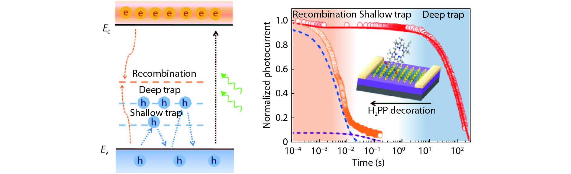
Fig. 1.
(Color online) Schematic diagram of carrier recombination and trapping kinetics (left) and transient response of as-prepared and H2PP decorated ReS2 photoconductor (right)[7].
NEWS AND VIEWS
Jie Jiang and Zhenhua Ni
Corresponding author: Z H Ni, zhni@seu.edu.cn
| [1] |
Hu Z, Wu Z, Han C, et al. Two-dimensional transition metal dichalcogenides: interface and defect engineering. Chem Soc Rev, 2018, 47, 3100 doi: 10.1039/C8CS00024G
|
| [2] |
Lien D H, Uddin S Z, Yeh M, et al. Electrical suppression of all nonradiative recombination pathways in monolayer semiconductors. Science, 2019, 364, 468 doi: 10.1126/science.aaw8053
|
| [3] |
Han H V, Lu A Y, Lu L S, et al. Photoluminescence enhancement and structure repairing of monolayer MoSe2 by hydrohalic acid treatment. ACS Nano, 2016, 10, 1454 doi: 10.1021/acsnano.5b06960
|
| [4] |
Nan H, Wang Z, Wang W, et al. Strong photoluminescence enhancement of MoS2 through defect engineering and oxygen bonding. ACS Nano, 2014, 8, 5738 doi: 10.1021/nn500532f
|
| [5] |
Yu Z, Pan Y, Shen Y, et al. Towards intrinsic charge transport in monolayer molybdenum disulfide by defect and interface engineering. Nat Commun, 2014, 5, 5290 doi: 10.1038/ncomms6290
|
| [6] |
Zhang X, Liao Q, Liu S, et al. Poly (4-styrenesulfonate)-induced sulfur vacancy self-healing strategy for monolayer MoS2 homojunction photodiode. Nat Commun, 2017, 8, 15881 doi: 10.1038/ncomms15881
|
| [7] |
Jiang J, Ling C, Xu T, et al. Defect engineering for modulating the trap states in 2D photoconductors. Adv Mater, 2018, 30, 1804332 doi: 10.1002/adma.v30.40
|
| [8] |
Tosun M, Chan L, Amani M, et al. Air-stable n-doping of WSe2 by anion vacancy formation with mild plasma treatment. ACS Nano, 2016, 10, 6853 doi: 10.1021/acsnano.6b02521
|
| [9] |
Giannazzo F, Fisichella G, Greco G, et al. Ambipolar MoS2 transistors by nanoscale tailoring of Schottky barrier using oxygen plasma functionalization. ACS Appl Mater Inter, 2017, 9, 23164 doi: 10.1021/acsami.7b04919
|


Article views: 4961 Times PDF downloads: 114 Times Cited by: 0 Times
Received: Revised: Online: Accepted Manuscript: 05 June 2019Uncorrected proof: 10 June 2019Published: 05 July 2019
| Citation: |
Jie Jiang, Zhenhua Ni. Defect engineering in two-dimensional materials[J]. Journal of Semiconductors, 2019, 40(7): 070403. doi: 10.1088/1674-4926/40/7/070403
****
J Jiang, Z H Ni, Defect engineering in two-dimensional materials[J]. J. Semicond., 2019, 40(7): 070403. doi: 10.1088/1674-4926/40/7/070403.

|
| [1] |
Hu Z, Wu Z, Han C, et al. Two-dimensional transition metal dichalcogenides: interface and defect engineering. Chem Soc Rev, 2018, 47, 3100 doi: 10.1039/C8CS00024G
|
| [2] |
Lien D H, Uddin S Z, Yeh M, et al. Electrical suppression of all nonradiative recombination pathways in monolayer semiconductors. Science, 2019, 364, 468 doi: 10.1126/science.aaw8053
|
| [3] |
Han H V, Lu A Y, Lu L S, et al. Photoluminescence enhancement and structure repairing of monolayer MoSe2 by hydrohalic acid treatment. ACS Nano, 2016, 10, 1454 doi: 10.1021/acsnano.5b06960
|
| [4] |
Nan H, Wang Z, Wang W, et al. Strong photoluminescence enhancement of MoS2 through defect engineering and oxygen bonding. ACS Nano, 2014, 8, 5738 doi: 10.1021/nn500532f
|
| [5] |
Yu Z, Pan Y, Shen Y, et al. Towards intrinsic charge transport in monolayer molybdenum disulfide by defect and interface engineering. Nat Commun, 2014, 5, 5290 doi: 10.1038/ncomms6290
|
| [6] |
Zhang X, Liao Q, Liu S, et al. Poly (4-styrenesulfonate)-induced sulfur vacancy self-healing strategy for monolayer MoS2 homojunction photodiode. Nat Commun, 2017, 8, 15881 doi: 10.1038/ncomms15881
|
| [7] |
Jiang J, Ling C, Xu T, et al. Defect engineering for modulating the trap states in 2D photoconductors. Adv Mater, 2018, 30, 1804332 doi: 10.1002/adma.v30.40
|
| [8] |
Tosun M, Chan L, Amani M, et al. Air-stable n-doping of WSe2 by anion vacancy formation with mild plasma treatment. ACS Nano, 2016, 10, 6853 doi: 10.1021/acsnano.6b02521
|
| [9] |
Giannazzo F, Fisichella G, Greco G, et al. Ambipolar MoS2 transistors by nanoscale tailoring of Schottky barrier using oxygen plasma functionalization. ACS Appl Mater Inter, 2017, 9, 23164 doi: 10.1021/acsami.7b04919
|

 WeChat ID
Journal of Semiconductors © 2017 All Rights Reserved 京ICP備05085259號-2
 DownLoad:

