


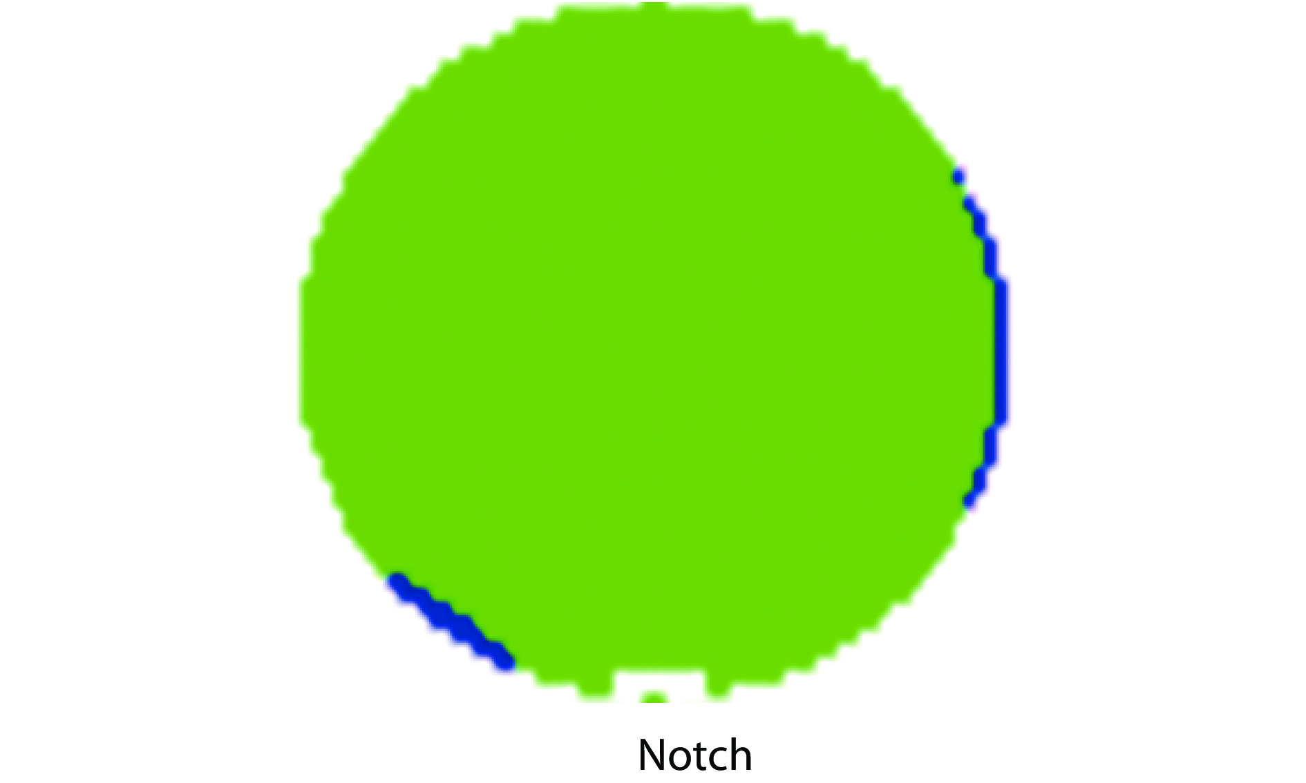
Fig. 1.
(Color online) Yield loss map induced by the CT open issue.
ARTICLES
Zhangli Liu, Bingkui He, Fei Meng, Qiang Bao, Yuhong Sun, Shaojun Sun, Guangwei Zhou, Xiuliang Cao and Haiwei Xin
Corresponding author: Zhangli Liu, Email: Zhangli.Liu@hhgrace.com
Abstract: Radio-frequency (RF) process products suffer from a wafer edge low yield issue, which is induced by contact opening. A failure mechanism has been proposed that is based on the characteristics of a wafer edge film stack. The large step height at the wafer’s edge leads to worse planarization for the sparse poly-pattern region during the inter-layer dielectric (ILD) chemical mechanical polishing (CMP) process. A thicker bottom anti-reflect coating (BARC) layer was introduced for a sparse poly-pattern at the wafer edge region. The contact open issue was solved by increasing the break through (BT) time to get a large enough window. Well profile and resistance uniformity were obtained by contact etch recipe optimization.
Key words: bottom anti-reflect coating, break through, wafer edge, planarization
| [1] |
Esfeh B K, Rack M, Ali K B, et al. RF small- and large-signal characteristics of CPW and TFMS lines on trap-rich HR-SOI substrates. IEEE Trans Electron Devices, 2018, 65, 3120 doi: 10.1109/TED.2018.2845679
|
| [2] |
Jaffe M, Abou-Khalil M, Botula A, et al. Improvements in SOI technology for RF switches. IEEE 15th Topical Meeting on Silicon Monolithic Integrated Circuits in RF Systems, 2015, 30
|
| [3] |
Gianesello F, Monroy A, Vialla V, et al. Highly linear and sub 120 fs Ron × Coff 130 nm RF SOI technology targeting 5G carrier aggregation RF switches and FEM SOC. IEEE 16th Topical Meeting on Silicon Monolithic Integrated Circuits in RF Systems (SiRF), 2016, 9
|
| [4] |
Maleville C, Celler G. SOI: Challenges and solutions to increasing yield in an ultrathin age. Yield Management Solutions, 2004, 6
|
| [5] |
Delahaye B, Baltzinger J L, Denis L, et al. Edge and extreme edge wafer manufacturing on 200 mm wafer: methodology, yield challenges, cost effective solutions, limitations. IEEE/SEMI Advanced Semiconductor Manufacturing Conference, 2009, 100
|
| [6] |
Goh I A N, Chua H S, Neo T L, et al. An integrated engineering approach to improve wafer edge yield. IEEE International Symposium on Semiconductor Manufacturing Conference Proceedings, 2001, 351
|
| [7] |
Harris K R, Ang B Y. Yield implications of wafer edge engineering. International Symposium on Microelectronics & Assembly, 2000, 70
|
| [8] |
Plummer J D, Deal M D, Griffin P B. Silicon VLSI technology. Beijing: Publishing House of Electronics Industry, 2003
|
| [9] |
Quirk M, Serda J. Semiconductor manufacturing technology. Beijing: Publishing House of Electronics Industry, 2006
|
| [10] |
Men Y W, Zhang H, Zhou K, et al. Wafer back pressure control and optimization in the CMP process. J Semicond, 2011, 32, 126002 doi: 10.1088/1674-4926/32/12/126002
|
| [11] |
Zhou J W, Liu Y L, Zhang W. Study of CMP lapping technique of ULSI silicon substrate. J Semicond, 2007, 28, 572
|
| [12] |
Boumerzoug M. Optimized BARC films and etch byproduct removal for wafer edge defectivity reduction. 25th Annual SEMI Advanced Semiconductor Manufacturing Conference, 2014, 330
|
| [13] |
Hu H S, Zhang M. Modeling for charging effect during RIE processing. Chin J Electron, 2000, 28, 81
|
| [14] |
Ding H T, Yang Z C, Yan G Z. A dual-purpose method to enhance heat transfer and prevent notching effect in deep reactive ion etching. Chin J Electron, 2010, 38, 1201
|
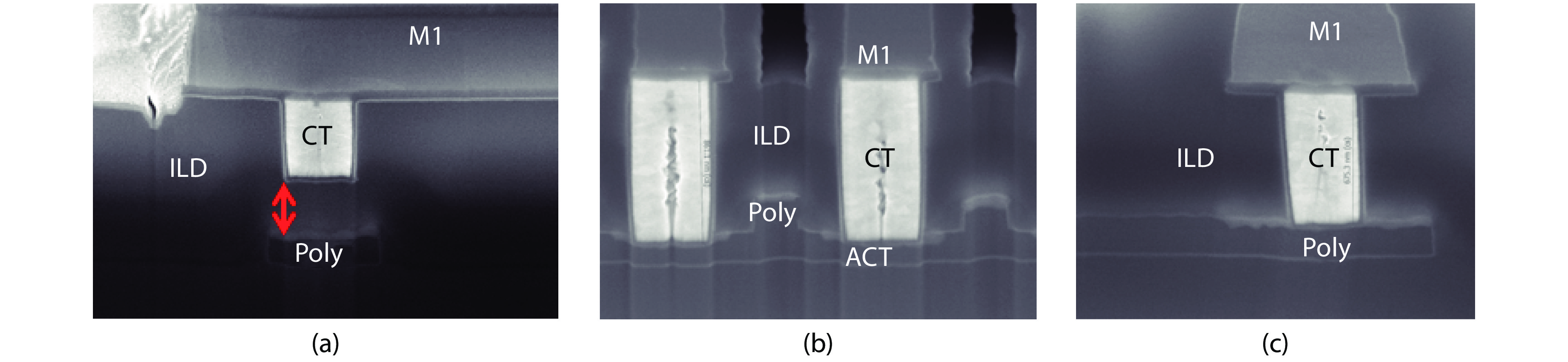
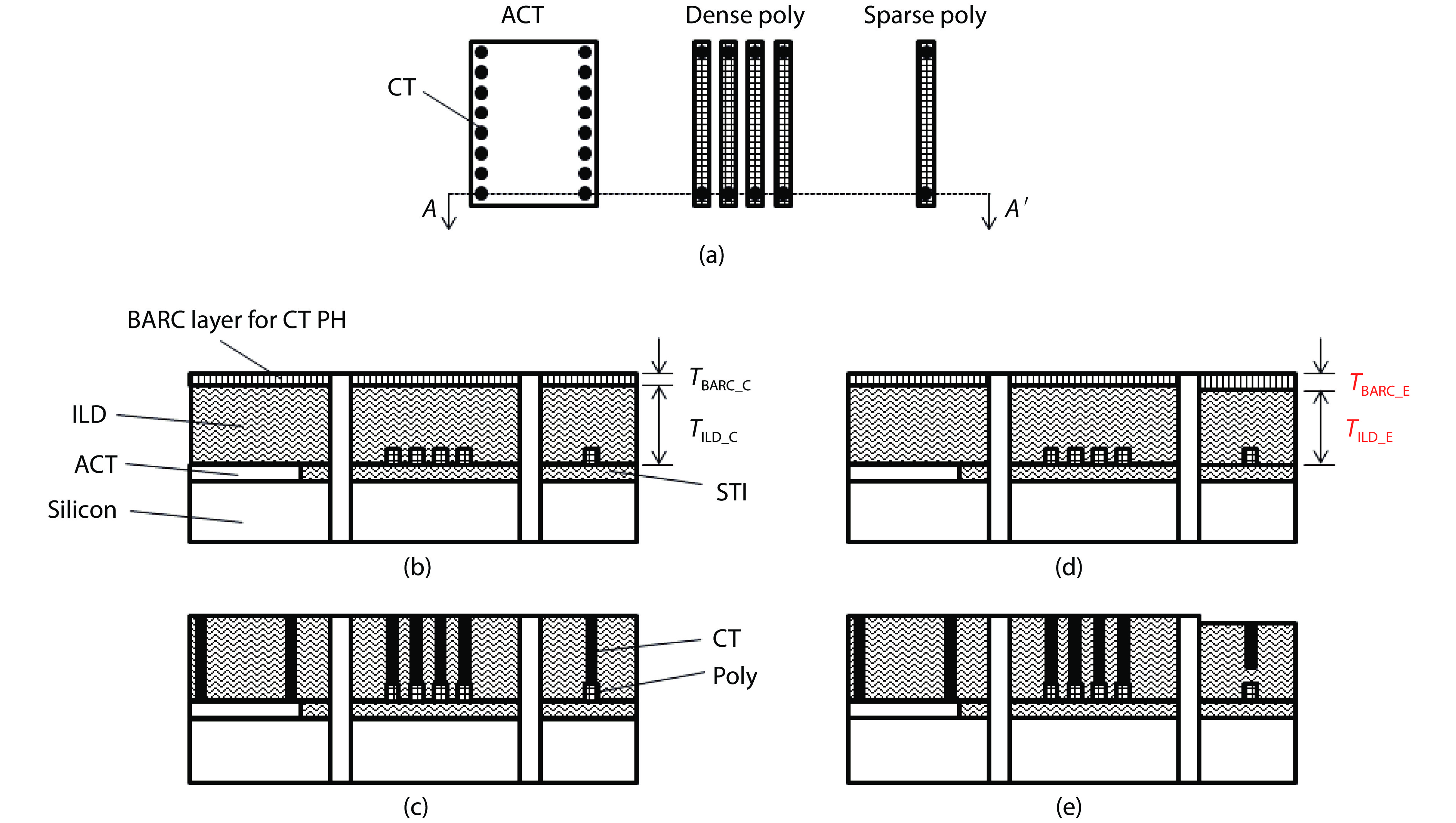
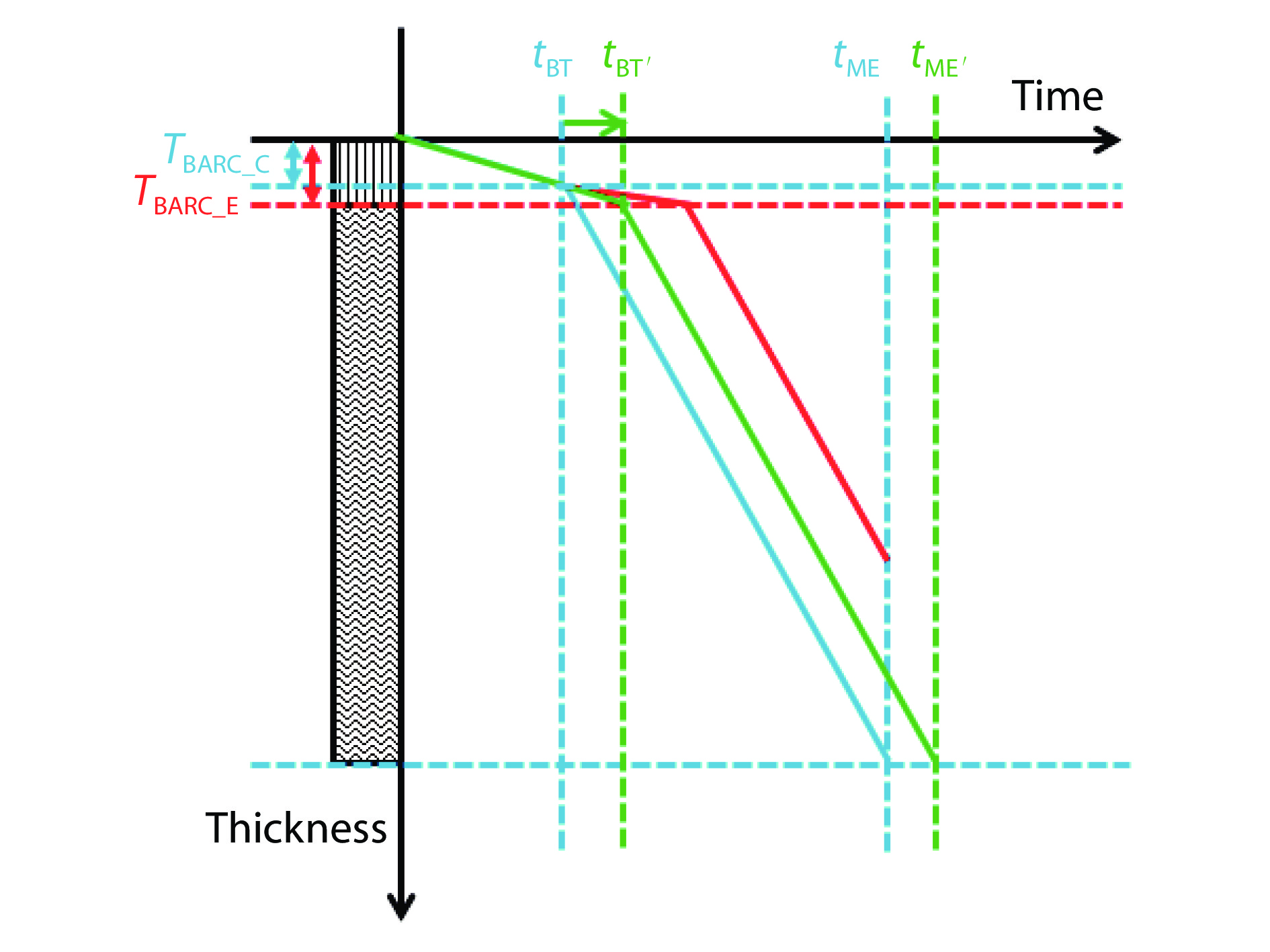
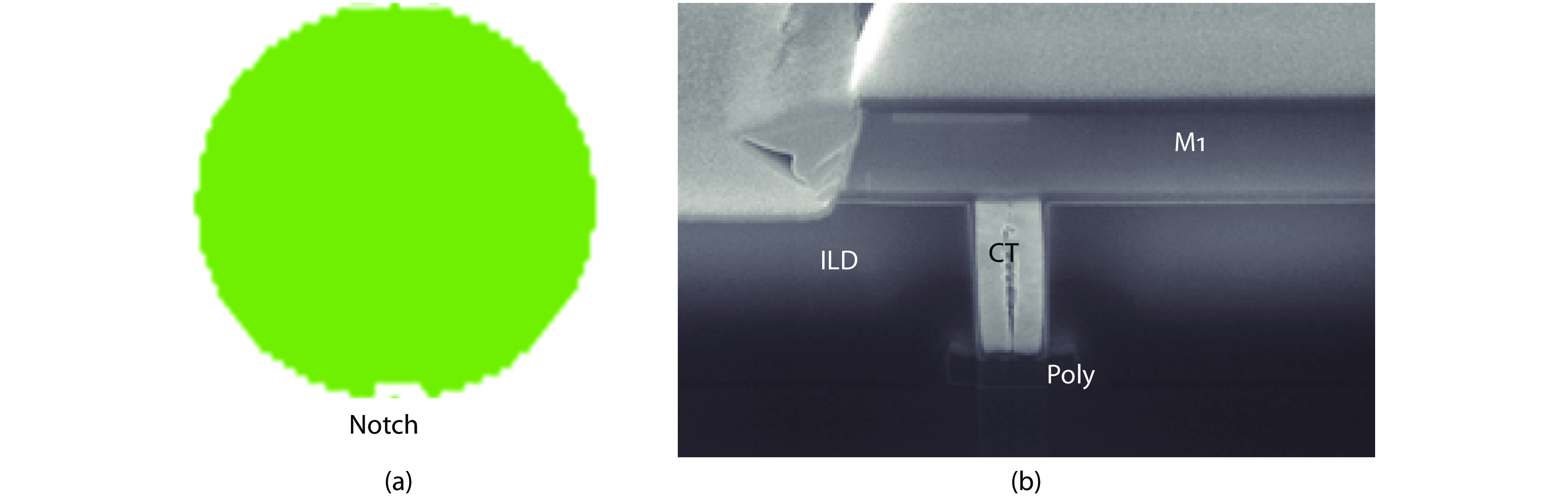
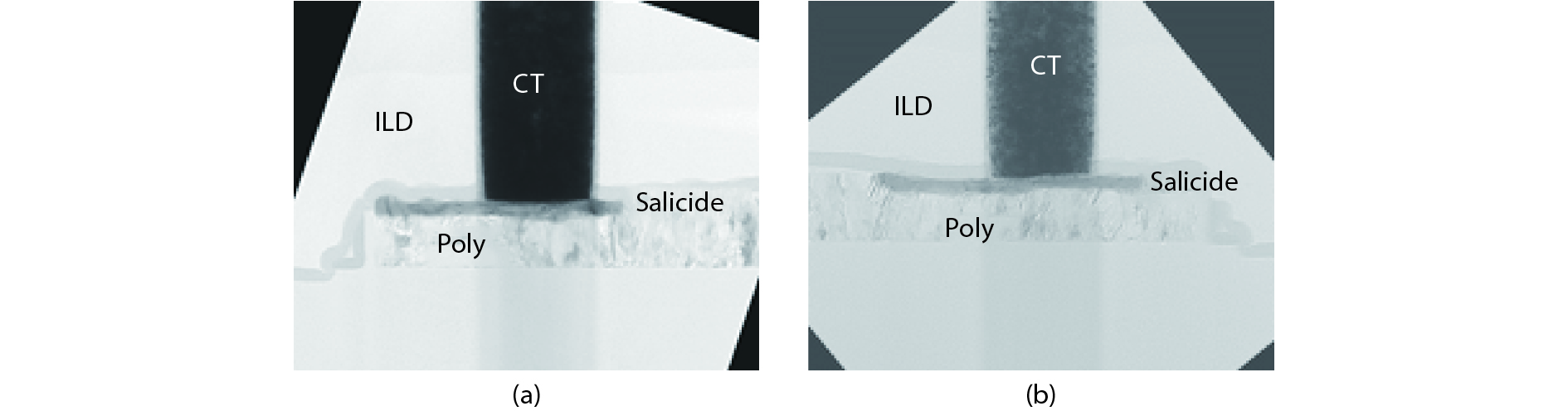
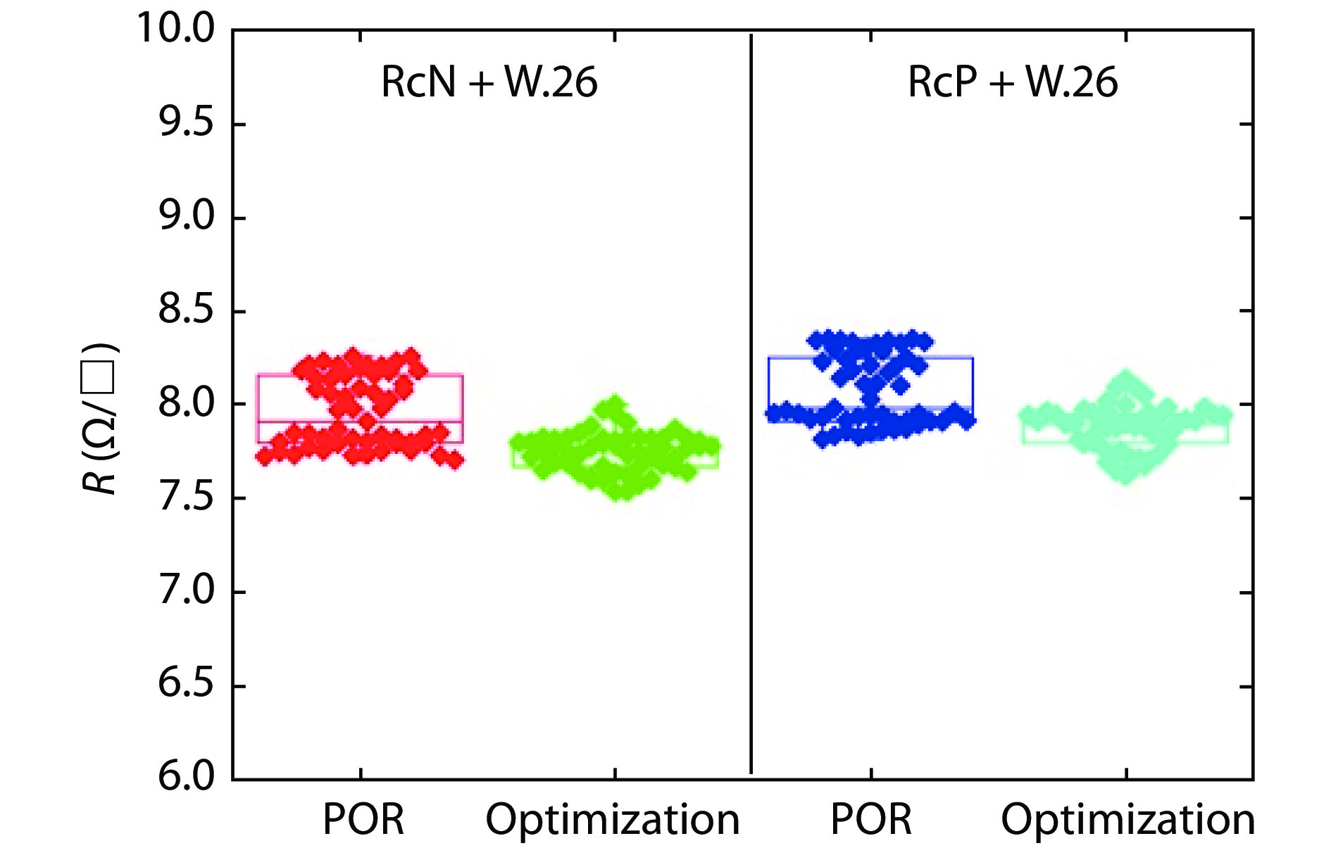
Table 1. Etch rate for BARC and ILD oxide.
| CT etch step | BARC | ILD oxide | |
| 1st step | BT (CF4 base) | 1 | 2.938 |
| 2nd step | ME (C5F8 base) | 0.102 | 1 |
 DownLoad: CSV
| [1] |
Esfeh B K, Rack M, Ali K B, et al. RF small- and large-signal characteristics of CPW and TFMS lines on trap-rich HR-SOI substrates. IEEE Trans Electron Devices, 2018, 65, 3120 doi: 10.1109/TED.2018.2845679
|
| [2] |
Jaffe M, Abou-Khalil M, Botula A, et al. Improvements in SOI technology for RF switches. IEEE 15th Topical Meeting on Silicon Monolithic Integrated Circuits in RF Systems, 2015, 30
|
| [3] |
Gianesello F, Monroy A, Vialla V, et al. Highly linear and sub 120 fs Ron × Coff 130 nm RF SOI technology targeting 5G carrier aggregation RF switches and FEM SOC. IEEE 16th Topical Meeting on Silicon Monolithic Integrated Circuits in RF Systems (SiRF), 2016, 9
|
| [4] |
Maleville C, Celler G. SOI: Challenges and solutions to increasing yield in an ultrathin age. Yield Management Solutions, 2004, 6
|
| [5] |
Delahaye B, Baltzinger J L, Denis L, et al. Edge and extreme edge wafer manufacturing on 200 mm wafer: methodology, yield challenges, cost effective solutions, limitations. IEEE/SEMI Advanced Semiconductor Manufacturing Conference, 2009, 100
|
| [6] |
Goh I A N, Chua H S, Neo T L, et al. An integrated engineering approach to improve wafer edge yield. IEEE International Symposium on Semiconductor Manufacturing Conference Proceedings, 2001, 351
|
| [7] |
Harris K R, Ang B Y. Yield implications of wafer edge engineering. International Symposium on Microelectronics & Assembly, 2000, 70
|
| [8] |
Plummer J D, Deal M D, Griffin P B. Silicon VLSI technology. Beijing: Publishing House of Electronics Industry, 2003
|
| [9] |
Quirk M, Serda J. Semiconductor manufacturing technology. Beijing: Publishing House of Electronics Industry, 2006
|
| [10] |
Men Y W, Zhang H, Zhou K, et al. Wafer back pressure control and optimization in the CMP process. J Semicond, 2011, 32, 126002 doi: 10.1088/1674-4926/32/12/126002
|
| [11] |
Zhou J W, Liu Y L, Zhang W. Study of CMP lapping technique of ULSI silicon substrate. J Semicond, 2007, 28, 572
|
| [12] |
Boumerzoug M. Optimized BARC films and etch byproduct removal for wafer edge defectivity reduction. 25th Annual SEMI Advanced Semiconductor Manufacturing Conference, 2014, 330
|
| [13] |
Hu H S, Zhang M. Modeling for charging effect during RIE processing. Chin J Electron, 2000, 28, 81
|
| [14] |
Ding H T, Yang Z C, Yan G Z. A dual-purpose method to enhance heat transfer and prevent notching effect in deep reactive ion etching. Chin J Electron, 2010, 38, 1201
|


Article views: 7667 Times PDF downloads: 149 Times Cited by: 0 Times
Received: 17 January 2019 Revised: 21 April 2019 Online: Accepted Manuscript: 26 August 2019Uncorrected proof: 28 August 2019Published: 09 December 2019
| Citation: |
Zhangli Liu, Bingkui He, Fei Meng, Qiang Bao, Yuhong Sun, Shaojun Sun, Guangwei Zhou, Xiuliang Cao, Haiwei Xin. Contact etch process optimization for RF process wafer edge yield improvement[J]. Journal of Semiconductors, 2019, 40(12): 122402. doi: 10.1088/1674-4926/40/12/122402
****
Z L Liu, B K He, F Meng, Q Bao, Y H Sun, S J Sun, G W Zhou, X L Cao, H W Xin, Contact etch process optimization for RF process wafer edge yield improvement[J]. J. Semicond., 2019, 40(12): 122402. doi: 10.1088/1674-4926/40/12/122402.

|
| [1] |
Esfeh B K, Rack M, Ali K B, et al. RF small- and large-signal characteristics of CPW and TFMS lines on trap-rich HR-SOI substrates. IEEE Trans Electron Devices, 2018, 65, 3120 doi: 10.1109/TED.2018.2845679
|
| [2] |
Jaffe M, Abou-Khalil M, Botula A, et al. Improvements in SOI technology for RF switches. IEEE 15th Topical Meeting on Silicon Monolithic Integrated Circuits in RF Systems, 2015, 30
|
| [3] |
Gianesello F, Monroy A, Vialla V, et al. Highly linear and sub 120 fs Ron × Coff 130 nm RF SOI technology targeting 5G carrier aggregation RF switches and FEM SOC. IEEE 16th Topical Meeting on Silicon Monolithic Integrated Circuits in RF Systems (SiRF), 2016, 9
|
| [4] |
Maleville C, Celler G. SOI: Challenges and solutions to increasing yield in an ultrathin age. Yield Management Solutions, 2004, 6
|
| [5] |
Delahaye B, Baltzinger J L, Denis L, et al. Edge and extreme edge wafer manufacturing on 200 mm wafer: methodology, yield challenges, cost effective solutions, limitations. IEEE/SEMI Advanced Semiconductor Manufacturing Conference, 2009, 100
|
| [6] |
Goh I A N, Chua H S, Neo T L, et al. An integrated engineering approach to improve wafer edge yield. IEEE International Symposium on Semiconductor Manufacturing Conference Proceedings, 2001, 351
|
| [7] |
Harris K R, Ang B Y. Yield implications of wafer edge engineering. International Symposium on Microelectronics & Assembly, 2000, 70
|
| [8] |
Plummer J D, Deal M D, Griffin P B. Silicon VLSI technology. Beijing: Publishing House of Electronics Industry, 2003
|
| [9] |
Quirk M, Serda J. Semiconductor manufacturing technology. Beijing: Publishing House of Electronics Industry, 2006
|
| [10] |
Men Y W, Zhang H, Zhou K, et al. Wafer back pressure control and optimization in the CMP process. J Semicond, 2011, 32, 126002 doi: 10.1088/1674-4926/32/12/126002
|
| [11] |
Zhou J W, Liu Y L, Zhang W. Study of CMP lapping technique of ULSI silicon substrate. J Semicond, 2007, 28, 572
|
| [12] |
Boumerzoug M. Optimized BARC films and etch byproduct removal for wafer edge defectivity reduction. 25th Annual SEMI Advanced Semiconductor Manufacturing Conference, 2014, 330
|
| [13] |
Hu H S, Zhang M. Modeling for charging effect during RIE processing. Chin J Electron, 2000, 28, 81
|
| [14] |
Ding H T, Yang Z C, Yan G Z. A dual-purpose method to enhance heat transfer and prevent notching effect in deep reactive ion etching. Chin J Electron, 2010, 38, 1201
|

 WeChat ID
Journal of Semiconductors © 2017 All Rights Reserved 京ICP備05085259號-2

