


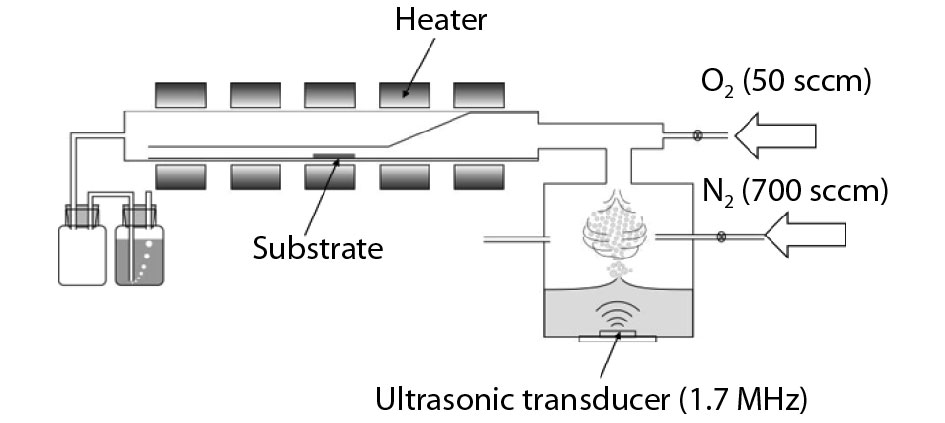
Fig. 1.
Schematic illustration the mist-CVD system used for α-Ga2O3 epitaxy.
ARTICLES
Tongchuan Ma, Xuanhu Chen, Fangfang Ren, Shunming Zhu, Shulin Gu, Rong Zhang, Youdou Zheng and Jiandong Ye
Corresponding author: Jiandong Ye, Email: yejd@nju.edu.cn
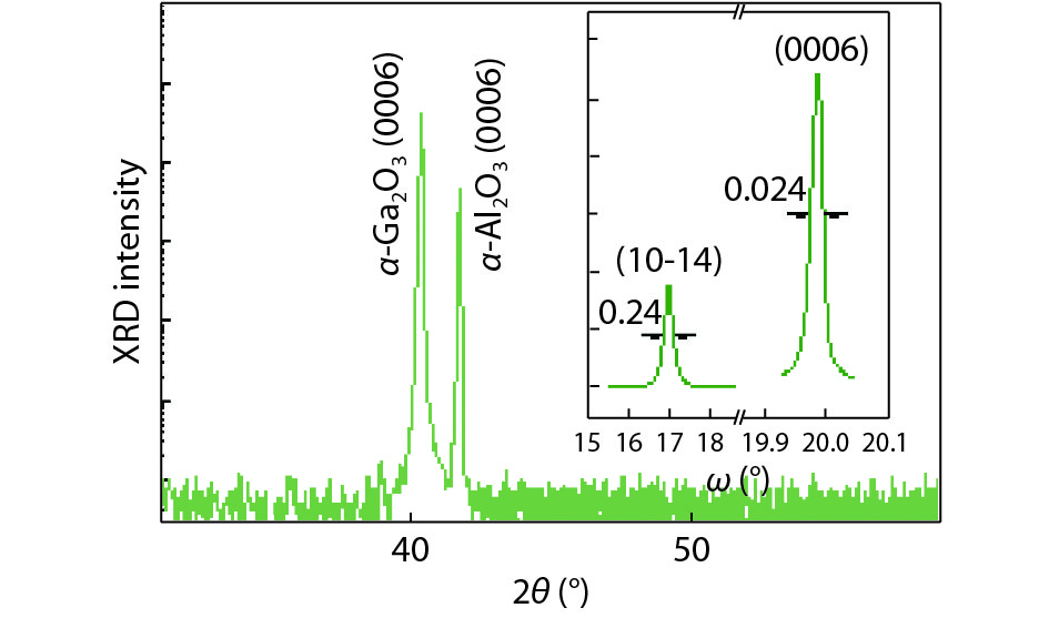
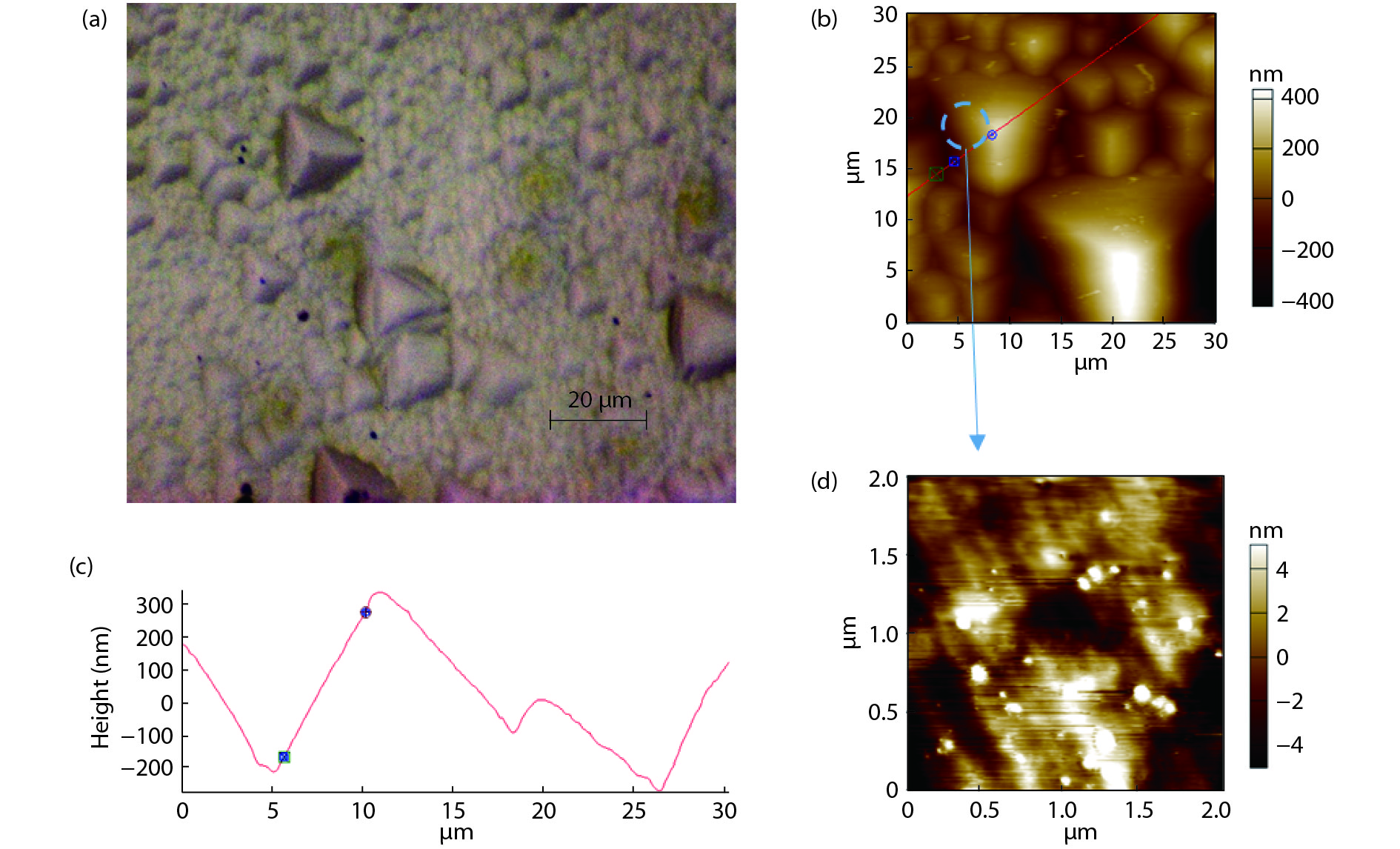
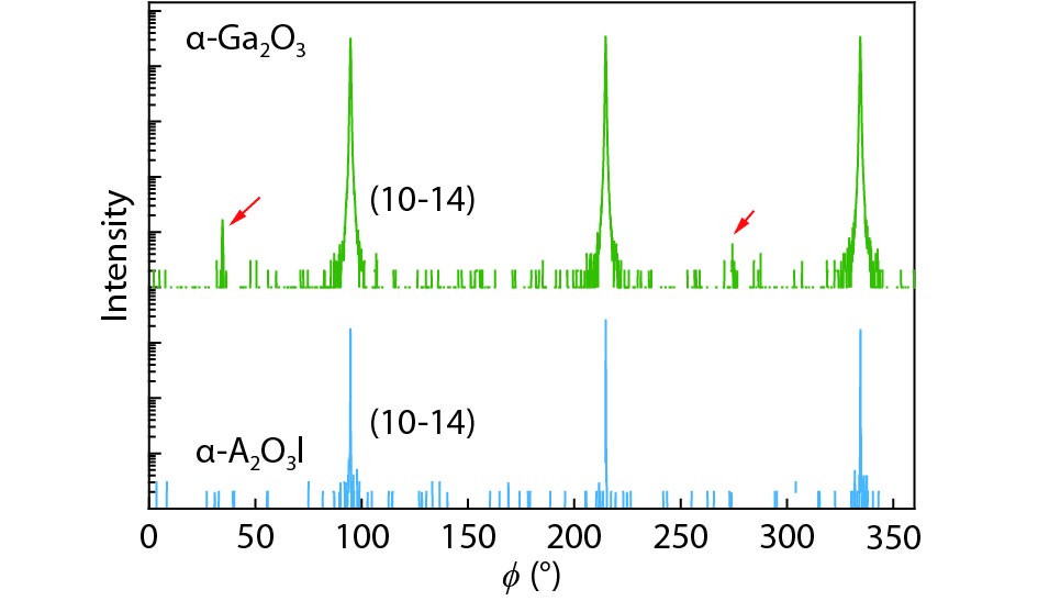
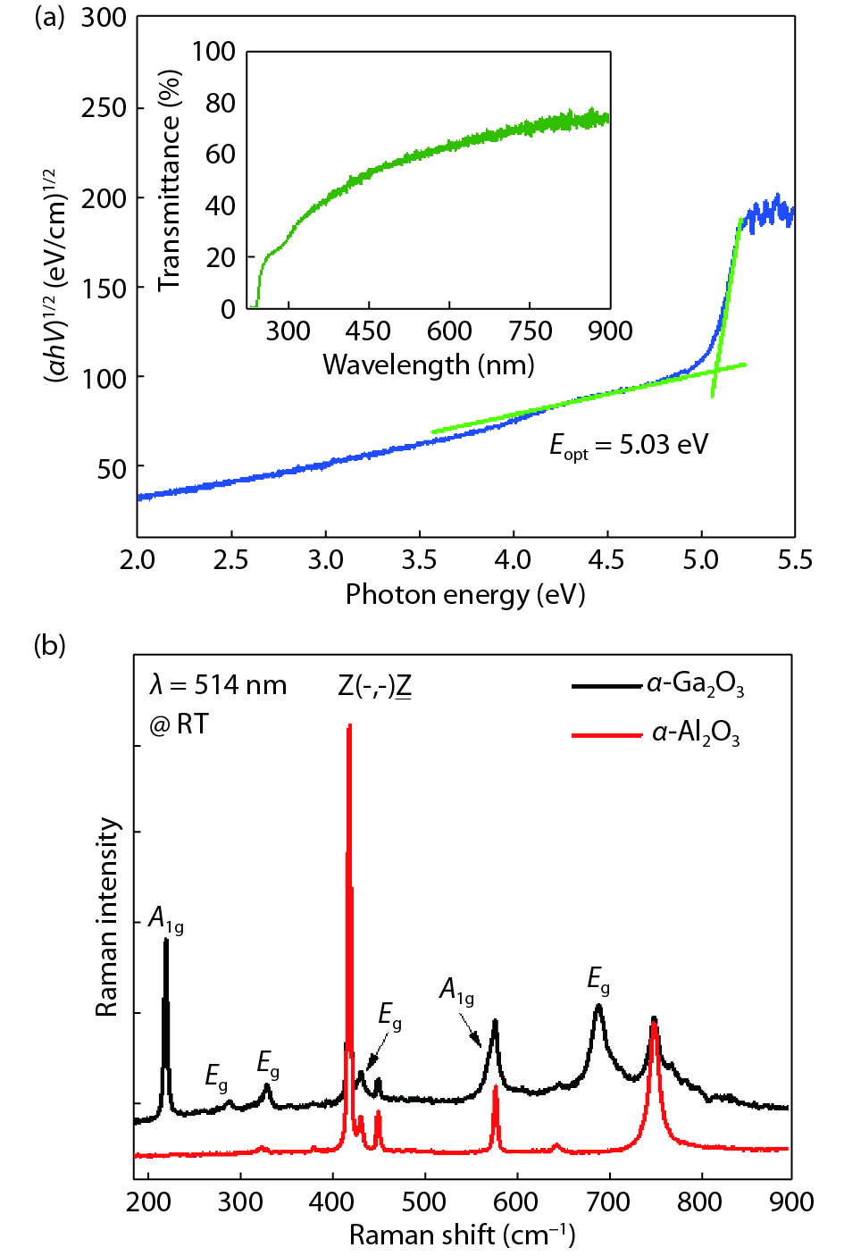
Abstract: The 8 μm thick single-crystalline α-Ga2O3 epilayers have been heteroepitaxially grown on sapphire (0001) substrates via mist chemical vapor deposition technique. High resolution X-ray diffraction measurements show that the full-widths-at-half-maximum (FWHM) of rocking curves for the (0006) and (10-14) planes are 0.024° and 0.24°, and the corresponding densities of screw and edge dislocations are 2.24 × 10⁶ and 1.63 × 109 cm?2, respectively, indicative of high single crystallinity. The out-of-plane and in-plane epitaxial relationships are [0001] α-Ga2O3//[0001] α-Al2O3 and [11-20] α-Ga2O3//[11-20] α-Al2O3, respectively. The lateral domain size is in micron scale and the indirect bandgap is determined as 5.03 eV by transmittance spectra. Raman measurement indicates that the lattice-mismatch induced compressive residual strain cannot be ruled out despite the large thickness of the α-Ga2O3 epilayer. The achieved high quality α-Ga2O3 may provide an alternative material platform for developing high performance power devices and solar-blind photodetectors.
Key words: ultra-wide bandgap semiconductor, chemical vapor deposition, epitaxy, gallium oxide
| [1] |
Varley J B, Weber J R, Janotti A, et al. Oxygen vacancies and donor impurities in β-Ga2O3. Appl Phys Lett, 2010, 97(14), 142106 doi: 10.1063/1.3499306
|
| [2] |
Higashiwaki M, Sasaki K, Kuramata A, et al. Gallium oxide (Ga2O3) metal-semiconductor field-effect transistors on single-crystal β-Ga2O3 (010) substrates. Appl Phys Lett, 2012, 100 (1), 013504 doi: 10.1063/1.3674287
|
| [3] |
Playford H Y, Hannon A C, Barney E R, et al.Structures of uncharacterised polymorphs of gallium oxide from total neutron diffraction. Chemistry, 2013, 19 (8), 2803 doi: 10.1002/chem.201203359
|
| [4] |
Roy R, Hill V G, Osborn E F. Polymorphism of Ga2O3 and the System Ga2O3-H2O. J Am Chem Soc, 1952, 74 (3), 719 doi: 10.1021/ja01123a039
|
| [5] |
Aida H, Nishiguchi K, Takeda H, et al. Growth of β-Ga2O3 single crystals by the edge-defined, film fed growth method. Jpn J Appl Phys, 2008, 47 (11), 8506 doi: 10.1143/JJAP.47.8506
|
| [6] |
Mahmoud W E. Solar blind avalanche photodetector based on the cation exchange growth of β-Ga2O3/SnO2 bilayer heterostructure thin film. Sol Energy Mater Sol Cells, 2016, 152, 65 doi: 10.1016/j.solmat.2016.03.015
|
| [7] |
Guo D Y, Shi H Z, Qian Y P, et al. Fabrication of β-Ga2O3/ZnO heterojunction for solar-blind deep ultraviolet photodetection. Semicond Sci Technol, 2017, 32 (3), 03LT01. doi: 10.1088/1361-6641/aa59b0
|
| [8] |
Zhao X, Wu Z, Guo D, et al. Growth and characterization of α-phase Ga2?xSnxO3 thin films for solar-blind ultraviolet applications. Semicond Sci Technol, 2016, 31 (6), 065010. doi: 10.1088/0268-1242/31/6/065010
|
| [9] |
Chen X, Xu Y, Zhou D, et al. Solar-blind photodetector with high avalanche gains and bias-tunable detecting functionality based on metastable phase alpha-Ga2O3/ZnO isotype heterostructures. ACS Appl Mater Interfaces, 2017, 9 (42), 36997 doi: 10.1021/acsami.7b09812
|
| [10] |
Li J, Chen X, Ma T, et al. Identification and modulation of electronic band structures of single-phase β-(AlxGa1?x)2O3 alloys grown by laser molecular beam epitaxy. Appl Phys Lett, 2018, 113 (4), 041901. doi: 10.1063/1.5027763
|
| [11] |
Zhao B, Wang F, Chen H, et al. Solar-blind avalanche photodetector based on single ZnO-Ga2O3 core-shell microwire. Nano Lett, 2015, 15 (6), 3988 doi: 10.1021/acs.nanolett.5b00906
|
| [12] |
Sasaki K, Higashiwaki M, Kuramata A, et al. Ga2O3 Schottky barrier diodes fabricated by using single-crystal β–Ga2O3 (010) substrates. IEEE Electron Device Lett, 2013, 34 (4), 493 doi: 10.1109/LED.2013.2244057
|
| [13] |
Akaiwa K, Fujita S. Electrical conductive corundum-structured α-Ga2O3 thin films on sapphire with tin-doping grown by spray-assisted mist chemical vapor deposition. J Jpn J Appl Phys, 2012, 51, 070203.
|
| [14] |
Ito H, Kaneko K, Fujita S. Growth and band gap control of corundum-structured α-Ga2O3 thin films on sapphire by spray-assisted mist chemical vapor deposition. Jpn J Appl Phys, 2012, 51, 100207.
|
| [15] |
Kaneko K, Nomura T, Kakeya I, et al. Fabrication of highly crystalline corundum-structured α-(Ga1?xFex)2O3 alloy thin films on sapphire substrates. Appl Phys Express 2009, 2, 075501.
|
| [16] |
Sun H, Li K H, Castanedo C G T, et al. HCl flow-induced phase change of α-, β-, and ε-Ga2O3 films grown by MOCVD. Cryst Growth Des. 2018, 18 (4), 2370 doi: 10.1021/acs.cgd.7b01791
|
| [17] |
Yao Y, Okur S, Lyle L A M, et al. Growth and characterization of α-, β-, and ?-phases of Ga2O3 using MOCVD and HVPE techniques. Mater Res Lett, 2018, 6 (5), 268 doi: 10.1080/21663831.2018.1443978
|
| [18] |
Kumaran R, Tiedje T, Webster S E, et al. Epitaxial Nd-doped alpha-(Al(1?x)Ga(x))2O3 films on sapphire for solid-state waveguide lasers. Opt Lett, 2010, 35 (22), 3793 doi: 10.1364/OL.35.003793
|
| [19] |
Fujita S, Oda M, Kaneko K, et al. Evolution of corundum-structured III-oxide semiconductors: Growth, properties, and devices. Jpn J Appl Phys, 2016, 55 (12), 1202A3. doi: 10.7567/JJAP.55.1202A3
|
| [20] |
Oda M, Kaneko K, Fujita S, et al. Crack-free thick (~5 μm) α-Ga2O3 films on sapphire substrates with α-(Al,Ga)2O3 buffer layers. Jpn J Appl Phys, 2016, 55 (12), 1202B4. doi: 10.7567/JJAP.55.1202B4
|
| [21] |
Shinohara D, Fujita S. Heteroepitaxy of corundum-structured α-Ga2O3 thin films on α-Al2O3 substrates by ultrasonic mist chemical vapor deposition. Jpn J Appl Phys, 2008, 47 (9), 7311 doi: 10.1143/JJAP.47.7311
|
| [22] |
Kawaharamura T. Physics on development of open-air atmospheric pressure thin film fabrication technique using mist droplets: Control of precursor flow. Jpn J Appl Phys, 2014, 53 (5), 05FF08.
|
| [23] |
Moram M A, Vickers M E. X-ray diffraction of III-nitrides. Rep Prog Phys, 2009, 72 (3), 036502. doi: 10.1088/0034-4885/72/3/036502
|
| [24] |
Zheng X H, Chen H, Yan Z B, et al. Determination of twist angle of in-plane mosaic spread of GaN films by high-resolution X-ray diffraction. J Cryst Growth, 2003, 255 (1/2), 63
|
| [25] |
Kaneko K, Kawanowa H, Ito H, et al. Evaluation of misfit relaxation in α-Ga2O3 epitaxial growth on α-Al2O3 substrate. Jpn J Appl Phys, 2012, 51, 020201.
|
| [26] |
Davis E A, Mott N F et al. Conduction in non-crystalline systems V. Conductivity, optical absorption and photoconductivity in amorphous semiconductors. Philos Mag A, 1970, 22 (179), 0903 doi: 10.1080/14786437008221061
|
| [27] |
Cusco R, Domenech-Amador N, Hatakeyama T, et al. Lattice dynamics of a mist-chemical vapor deposition-grown corundum-like Ga2O3 single crystal. J Appl Phys, 2015, 117 (18), 185706. doi: 10.1063/1.4921060
|


Article views: 7063 Times PDF downloads: 384 Times Cited by: 0 Times
Received: 01 August 2018 Revised: 13 September 2018 Online: Accepted Manuscript: 06 December 2018Uncorrected proof: 10 December 2018Published: 07 January 2019
| Citation: |
Tongchuan Ma, Xuanhu Chen, Fangfang Ren, Shunming Zhu, Shulin Gu, Rong Zhang, Youdou Zheng, Jiandong Ye. Heteroepitaxial growth of thick α-Ga2O3 film on sapphire (0001) by MIST-CVD technique[J]. Journal of Semiconductors, 2019, 40(1): 012804. doi: 10.1088/1674-4926/40/1/012804
****
T C Ma, X H Chen, F F Ren, S M Zhu, S L Gu, R Zhang, Y D Zheng, J D Ye, Heteroepitaxial growth of thick α-Ga2O3 film on sapphire (0001) by MIST-CVD technique[J]. J. Semicond., 2019, 40(1): 012804. doi: 10.1088/1674-4926/40/1/012804.

|
| [1] |
Varley J B, Weber J R, Janotti A, et al. Oxygen vacancies and donor impurities in β-Ga2O3. Appl Phys Lett, 2010, 97(14), 142106 doi: 10.1063/1.3499306
|
| [2] |
Higashiwaki M, Sasaki K, Kuramata A, et al. Gallium oxide (Ga2O3) metal-semiconductor field-effect transistors on single-crystal β-Ga2O3 (010) substrates. Appl Phys Lett, 2012, 100 (1), 013504 doi: 10.1063/1.3674287
|
| [3] |
Playford H Y, Hannon A C, Barney E R, et al.Structures of uncharacterised polymorphs of gallium oxide from total neutron diffraction. Chemistry, 2013, 19 (8), 2803 doi: 10.1002/chem.201203359
|
| [4] |
Roy R, Hill V G, Osborn E F. Polymorphism of Ga2O3 and the System Ga2O3-H2O. J Am Chem Soc, 1952, 74 (3), 719 doi: 10.1021/ja01123a039
|
| [5] |
Aida H, Nishiguchi K, Takeda H, et al. Growth of β-Ga2O3 single crystals by the edge-defined, film fed growth method. Jpn J Appl Phys, 2008, 47 (11), 8506 doi: 10.1143/JJAP.47.8506
|
| [6] |
Mahmoud W E. Solar blind avalanche photodetector based on the cation exchange growth of β-Ga2O3/SnO2 bilayer heterostructure thin film. Sol Energy Mater Sol Cells, 2016, 152, 65 doi: 10.1016/j.solmat.2016.03.015
|
| [7] |
Guo D Y, Shi H Z, Qian Y P, et al. Fabrication of β-Ga2O3/ZnO heterojunction for solar-blind deep ultraviolet photodetection. Semicond Sci Technol, 2017, 32 (3), 03LT01. doi: 10.1088/1361-6641/aa59b0
|
| [8] |
Zhao X, Wu Z, Guo D, et al. Growth and characterization of α-phase Ga2?xSnxO3 thin films for solar-blind ultraviolet applications. Semicond Sci Technol, 2016, 31 (6), 065010. doi: 10.1088/0268-1242/31/6/065010
|
| [9] |
Chen X, Xu Y, Zhou D, et al. Solar-blind photodetector with high avalanche gains and bias-tunable detecting functionality based on metastable phase alpha-Ga2O3/ZnO isotype heterostructures. ACS Appl Mater Interfaces, 2017, 9 (42), 36997 doi: 10.1021/acsami.7b09812
|
| [10] |
Li J, Chen X, Ma T, et al. Identification and modulation of electronic band structures of single-phase β-(AlxGa1?x)2O3 alloys grown by laser molecular beam epitaxy. Appl Phys Lett, 2018, 113 (4), 041901. doi: 10.1063/1.5027763
|
| [11] |
Zhao B, Wang F, Chen H, et al. Solar-blind avalanche photodetector based on single ZnO-Ga2O3 core-shell microwire. Nano Lett, 2015, 15 (6), 3988 doi: 10.1021/acs.nanolett.5b00906
|
| [12] |
Sasaki K, Higashiwaki M, Kuramata A, et al. Ga2O3 Schottky barrier diodes fabricated by using single-crystal β–Ga2O3 (010) substrates. IEEE Electron Device Lett, 2013, 34 (4), 493 doi: 10.1109/LED.2013.2244057
|
| [13] |
Akaiwa K, Fujita S. Electrical conductive corundum-structured α-Ga2O3 thin films on sapphire with tin-doping grown by spray-assisted mist chemical vapor deposition. J Jpn J Appl Phys, 2012, 51, 070203.
|
| [14] |
Ito H, Kaneko K, Fujita S. Growth and band gap control of corundum-structured α-Ga2O3 thin films on sapphire by spray-assisted mist chemical vapor deposition. Jpn J Appl Phys, 2012, 51, 100207.
|
| [15] |
Kaneko K, Nomura T, Kakeya I, et al. Fabrication of highly crystalline corundum-structured α-(Ga1?xFex)2O3 alloy thin films on sapphire substrates. Appl Phys Express 2009, 2, 075501.
|
| [16] |
Sun H, Li K H, Castanedo C G T, et al. HCl flow-induced phase change of α-, β-, and ε-Ga2O3 films grown by MOCVD. Cryst Growth Des. 2018, 18 (4), 2370 doi: 10.1021/acs.cgd.7b01791
|
| [17] |
Yao Y, Okur S, Lyle L A M, et al. Growth and characterization of α-, β-, and ?-phases of Ga2O3 using MOCVD and HVPE techniques. Mater Res Lett, 2018, 6 (5), 268 doi: 10.1080/21663831.2018.1443978
|
| [18] |
Kumaran R, Tiedje T, Webster S E, et al. Epitaxial Nd-doped alpha-(Al(1?x)Ga(x))2O3 films on sapphire for solid-state waveguide lasers. Opt Lett, 2010, 35 (22), 3793 doi: 10.1364/OL.35.003793
|
| [19] |
Fujita S, Oda M, Kaneko K, et al. Evolution of corundum-structured III-oxide semiconductors: Growth, properties, and devices. Jpn J Appl Phys, 2016, 55 (12), 1202A3. doi: 10.7567/JJAP.55.1202A3
|
| [20] |
Oda M, Kaneko K, Fujita S, et al. Crack-free thick (~5 μm) α-Ga2O3 films on sapphire substrates with α-(Al,Ga)2O3 buffer layers. Jpn J Appl Phys, 2016, 55 (12), 1202B4. doi: 10.7567/JJAP.55.1202B4
|
| [21] |
Shinohara D, Fujita S. Heteroepitaxy of corundum-structured α-Ga2O3 thin films on α-Al2O3 substrates by ultrasonic mist chemical vapor deposition. Jpn J Appl Phys, 2008, 47 (9), 7311 doi: 10.1143/JJAP.47.7311
|
| [22] |
Kawaharamura T. Physics on development of open-air atmospheric pressure thin film fabrication technique using mist droplets: Control of precursor flow. Jpn J Appl Phys, 2014, 53 (5), 05FF08.
|
| [23] |
Moram M A, Vickers M E. X-ray diffraction of III-nitrides. Rep Prog Phys, 2009, 72 (3), 036502. doi: 10.1088/0034-4885/72/3/036502
|
| [24] |
Zheng X H, Chen H, Yan Z B, et al. Determination of twist angle of in-plane mosaic spread of GaN films by high-resolution X-ray diffraction. J Cryst Growth, 2003, 255 (1/2), 63
|
| [25] |
Kaneko K, Kawanowa H, Ito H, et al. Evaluation of misfit relaxation in α-Ga2O3 epitaxial growth on α-Al2O3 substrate. Jpn J Appl Phys, 2012, 51, 020201.
|
| [26] |
Davis E A, Mott N F et al. Conduction in non-crystalline systems V. Conductivity, optical absorption and photoconductivity in amorphous semiconductors. Philos Mag A, 1970, 22 (179), 0903 doi: 10.1080/14786437008221061
|
| [27] |
Cusco R, Domenech-Amador N, Hatakeyama T, et al. Lattice dynamics of a mist-chemical vapor deposition-grown corundum-like Ga2O3 single crystal. J Appl Phys, 2015, 117 (18), 185706. doi: 10.1063/1.4921060
|

 WeChat ID
Journal of Semiconductors © 2017 All Rights Reserved 京ICP備05085259號-2
 DownLoad:

