


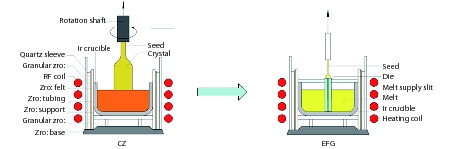
Fig. 1.
(Color online) Schematic of CZ and EFG process.
NEWS AND VIEWS
Corresponding author: Xutang Tao, txt@sdu.edu.cn
| [1] |
Higashiwaki M, Jessen G H. Guest Editorial: the dawn of gallium oxide microelectronics. Appl Phys Lett, 2018, 112, 060401 doi: 10.1063/1.5017845
|
| [2] |
Baldini M, Galazka Z, Wagner G. Recent progress in the growth of β-Ga2O3 for power electronics applications. Materials Science in Semiconductor Processing, 2018, 78, 132?146 doi: 10.1016/j.mssp.2017.10.040
|
| [3] |
Aida H, Nishiguchi K, Takeda H, et al. Growth of β-Ga2O3 single crystals by the edge-defined, film fed growth method. Jpn J Appl Phys, 2008, 47(11), 8506?8509 doi: 10.1143/JJAP.47.8506
|
| [4] |
Tomm Y, Reiche P, Klimm D, et al. Czochralski grown Ga2O3 crystals. J Cryst Growth, 2000, 220(4), 510 doi: 10.1016/S0022-0248(00)00851-4
|
| [5] |
Mastro M A, Kuramata A, Calkins J, et al. Opportunities and future directions for Ga2O3. ECS Journal of Solid State Science and Technology, 2017, 6(5), 356?359 doi: 10.1149/2.0031707jss
|
Table 1. Features of melt growth methods used for growing bulk β-Ga2O3 crystals.
| Method | Crystal shape | Crystal size (mm) | Growth direction | Crucible | Structural quality | Scalability |
| Verneuil | Cylinder | 9 × 25 | (100) plane | None | Poor | Limited |
| OFZ | Cylinder | 6 × 50
25 × 50 |
<100> | None | Acceptable | Limited |
| <010> | ||||||
| <001> | ||||||
| EFG | Slab | 50 × 75 × 3 | <010> | Ir | Good | High |
| 60 × 55 × 18 | ||||||
| 110 × 110 × 6 | ||||||
| VGF | Cylinder | 50 × 30 | <010> | Ir | Acceptable | High |
| VB | Cylinder | 25 × 25 | ⊥(100) | Pt?Rh | Acceptable | High |
| CZ | Cylinder | 10 × 30 | <010> | Ir | Good | High |
| 20 × 70 | ||||||
| 50 × 85 | ||||||
| Abbreviations: OFZ, optical floating zone; EFG, edge defined film-fed growth; VGF, vertical gradient freeze; VB, vertical bridgman; CZ, Czochralski. | ||||||
 DownLoad: CSV
| [1] |
Higashiwaki M, Jessen G H. Guest Editorial: the dawn of gallium oxide microelectronics. Appl Phys Lett, 2018, 112, 060401 doi: 10.1063/1.5017845
|
| [2] |
Baldini M, Galazka Z, Wagner G. Recent progress in the growth of β-Ga2O3 for power electronics applications. Materials Science in Semiconductor Processing, 2018, 78, 132?146 doi: 10.1016/j.mssp.2017.10.040
|
| [3] |
Aida H, Nishiguchi K, Takeda H, et al. Growth of β-Ga2O3 single crystals by the edge-defined, film fed growth method. Jpn J Appl Phys, 2008, 47(11), 8506?8509 doi: 10.1143/JJAP.47.8506
|
| [4] |
Tomm Y, Reiche P, Klimm D, et al. Czochralski grown Ga2O3 crystals. J Cryst Growth, 2000, 220(4), 510 doi: 10.1016/S0022-0248(00)00851-4
|
| [5] |
Mastro M A, Kuramata A, Calkins J, et al. Opportunities and future directions for Ga2O3. ECS Journal of Solid State Science and Technology, 2017, 6(5), 356?359 doi: 10.1149/2.0031707jss
|


Article views: 6318 Times PDF downloads: 245 Times Cited by: 0 Times
Received: 13 August 2018 Revised: 08 October 2018 Online: Accepted Manuscript: 08 January 2019Uncorrected proof: 09 January 2019Published: 07 January 2019
| Citation: |
Xutang Tao. Bulk gallium oxide single crystal growth[J]. Journal of Semiconductors, 2019, 40(1): 010401. doi: 10.1088/1674-4926/40/1/010401
****
X T Tao, Bulk gallium oxide single crystal growth[J]. J. Semicond., 2019, 40(1): 010401. doi: 10.1088/1674-4926/40/1/010401.

|
| [1] |
Higashiwaki M, Jessen G H. Guest Editorial: the dawn of gallium oxide microelectronics. Appl Phys Lett, 2018, 112, 060401 doi: 10.1063/1.5017845
|
| [2] |
Baldini M, Galazka Z, Wagner G. Recent progress in the growth of β-Ga2O3 for power electronics applications. Materials Science in Semiconductor Processing, 2018, 78, 132?146 doi: 10.1016/j.mssp.2017.10.040
|
| [3] |
Aida H, Nishiguchi K, Takeda H, et al. Growth of β-Ga2O3 single crystals by the edge-defined, film fed growth method. Jpn J Appl Phys, 2008, 47(11), 8506?8509 doi: 10.1143/JJAP.47.8506
|
| [4] |
Tomm Y, Reiche P, Klimm D, et al. Czochralski grown Ga2O3 crystals. J Cryst Growth, 2000, 220(4), 510 doi: 10.1016/S0022-0248(00)00851-4
|
| [5] |
Mastro M A, Kuramata A, Calkins J, et al. Opportunities and future directions for Ga2O3. ECS Journal of Solid State Science and Technology, 2017, 6(5), 356?359 doi: 10.1149/2.0031707jss
|

 WeChat ID
Journal of Semiconductors © 2017 All Rights Reserved 京ICP備05085259號(hào)-2

