


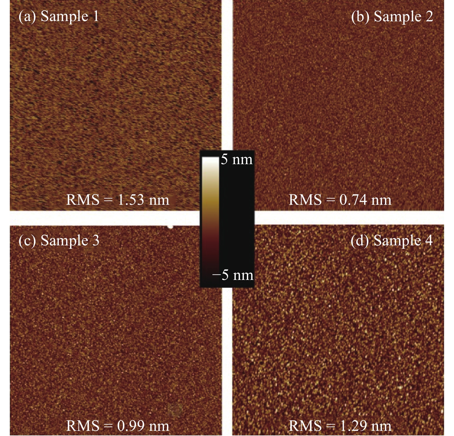
Fig. 1.
(Color online) AFM images of the SiNx samples with NH3 flow rate of (a) 3 sccm, (b) 6 sccm, (c) 9.5 sccm, and (d) 12 sccm, respectively (scanning area: 5 × 5 μm2).
SEMICONDUCTOR MATERIALS
Yi Zhu1, 2, Xingyou Chen1, Yingjie Ma1, Yonggang Zhang1, Ben Du1, 2, Yanhui Shi1, 2 and Yi Gu1,
Corresponding author: Yi Gu, Email: ygu@mail.sim.ac.cn
Abstract: The surface and optical properties of silicon nitride samples with different compositions were investigated. The samples were deposited on InP by inductively coupled plasma chemical vapor deposition using different NH3 flow rates. Atomic force microscopy measurements show that the surface roughness is increased for the samples with both low and high NH3 flow rates. By optimization, when the NH3 flow rate is 6 sccm, a smooth surface with RMS roughness of 0.74 nm over a 5 × 5 μm2 area has been achieved. X-ray photoelectron spectroscopy measurements reveal the Si/N ratio of the samples as a function of NH3 flow rate. It is found that amorphous silicon is dominant in the samples with low NH3 flow rates, which is also proved in Raman measurements. The bonding energies of the Si and N atoms have been extracted and analyzed. Results show that the bonding states of Si atoms transfer from Si0 to Si+4 as the NH3 flow rate increases.
Key words: silicon nitride, ICPCVD, X-ray photoelectron spectroscopy, Raman
| [1] |
Yota J, Hander J, Saleh A A. A comparative study on inductively-coupled plasma high-density plasma, plasma-enhanced and low pressure chemical vapor deposition silicon nitride films. J Vac Sci Technol A, 2000, 18(2): 372 doi: 10.1116/1.582195
|
| [2] |
Lee S H, Lee I, Yi J. Silicon nitride films prepared by high-density plasma chemical vapor deposition for solar cell applications. Surf Coat Technol, 2002, 153(1): 67 doi: 10.1016/S0257-8972(01)01554-7
|
| [3] |
Medjdoub M, Courant J L, Maher H, et al. Inductively coupled plasma-plasma enhanced chemical vapor deposition silicon nitride for passivation of InP based high electron mobility transistors (HEMTs). Mater Sci Eng B, 2001, 80(1): 252
|
| [4] |
Zhang J, Umana-Membreno G A, Gu R, et al. Investigation of ICPECVD silicon nitride films for HgCdTe surface passivation. J Electron Mater, 2015, 44(9): 2990 doi: 10.1007/s11664-015-3703-y
|
| [5] |
Shi M, Shao X M, Tang H J, et al. Inductively coupled plasma chemical vapor deposition silicon nitride for passivation of In0.83Ga0.17As photodiodes. Infrared Phys Technol, 2014, 67: 197 doi: 10.1016/j.infrared.2014.06.003
|
| [6] |
Wei P, Li X, Li T, et al. Surface passivation of In0.83Ga0.17As photodiode with high-quality SiN layer fabricated by ICPCVD at the lower temperature. Infrared Phys Technol, 2014, 62: 13 doi: 10.1016/j.infrared.2013.10.003
|
| [7] |
Wang H, Ng G I, Yang H, et al. Ammonia (NH3) plasma surface passivation of InP/InGaAs heterojunction bipolar transistors. International Conference on Indium Phosphide and Related Materials, 2001: 421
|
| [8] |
Moriguchi H, Hoshi S, Ohshima T, et al. Isolation degradation of InAlAs/InGaAs/InP HEMTs due to bias stress depending on passivation films formed by PCVD. International Conference on Indium Phosphide and Related Materials, 2001: 417
|
| [9] |
Wang H, Ng G I, Yang H, et al. Understanding the degradation of InP/InGaAs heterojunction bipolar transistors induced by silicon nitride passivation. International Conference on Indium Phosphide and Related Materials, 2001: 252
|
| [10] |
Jin Z, Uchida K, Nozaki S, et al. Passivation of InP-based HBTs. Appl Surf Sci, 2006, 252(21): 7664 doi: 10.1016/j.apsusc.2006.03.050
|
| [11] |
Lee J W, Mackenzie K D, Johnson D, et al. Low temperature silicon nitride and silicon dioxide film processing by inductively coupled plasma chemical vapor deposition. J Electrochem Soc, 2000, 147(4): 1481 doi: 10.1149/1.1393382
|
| [12] |
Chou Y C, Lai R, Li G P, et al. Innovative nitride passivated pseudomorphic GaAs HEMTs. IEEE Electron Device Lett, 2003, 24(1): 7 doi: 10.1109/LED.2002.807313
|
| [13] |
Wolf R, Wandel K, Gruska B. Low-temperature ICPECVD of silicon nitride in SiH4-NH3-Ar discharges analyzed by spectroscopic ellipsometry and etch behavior in KOH and BHF. Surf Coat Technol, 2001, 142: 786
|
| [14] |
Shi M, Tang H J, Shao X M, et al. Interface property of silicon nitride films grown by inductively coupled plasma chemical vapor deposition and plasma enhanced chemical vapor deposition on In0.82Al0.18As. Infrared Phys Technol, 2015, 71: 384 doi: 10.1016/j.infrared.2015.04.011
|
| [15] |
Dekkers H F W, Wolf D S, Agostinelli G, et al. Requirements of PECVD SiNx:H layers for bulk passivation of mc-Si. Sol Energy Mater Sol Cells, 2006, 90(18): 3244
|
| [16] |
Knotter D M, Denteneer T J J. Etching mechanism of silicon nitride in HF-based solutions. J Electrochem Soc, 2001, 148(3): F43 doi: 10.1149/1.1348262
|
| [17] |
Karcher R, Ley L, Johnson R L. Electronic structure of hydrogenated and unhydrogenated amorphous SiNx (0 ≤ x ≤1.6): A photoemission study. Phys Rev B, 1984, 30(4): 1896 doi: 10.1103/PhysRevB.30.1896
|
| [18] |
Moulder J F, Stickle W F, Sobol P E, et al. Handbook of X-ray photoelectron spectroscopy. Eden Prairie: Physical Electronics, 1992
|
| [19] |
Korchagina T T, Marin D V, Volodin V A, et al. Structure and optical properties of SiNx:H films with Si nanoclusters produced by low-frequency plasma-enhanced chemical vapor deposition. Semiconductors, 2009, 43(11): 1514 doi: 10.1134/S1063782609110207
|
| [20] |
Wei W S, Xu G Y, Wang J L, et al. Raman spectra of intrinsic and doped hydrogenated nanocrystalline silicon films. Vacuum, 2007, 81(5): 656 doi: 10.1016/j.vacuum.2006.09.006
|
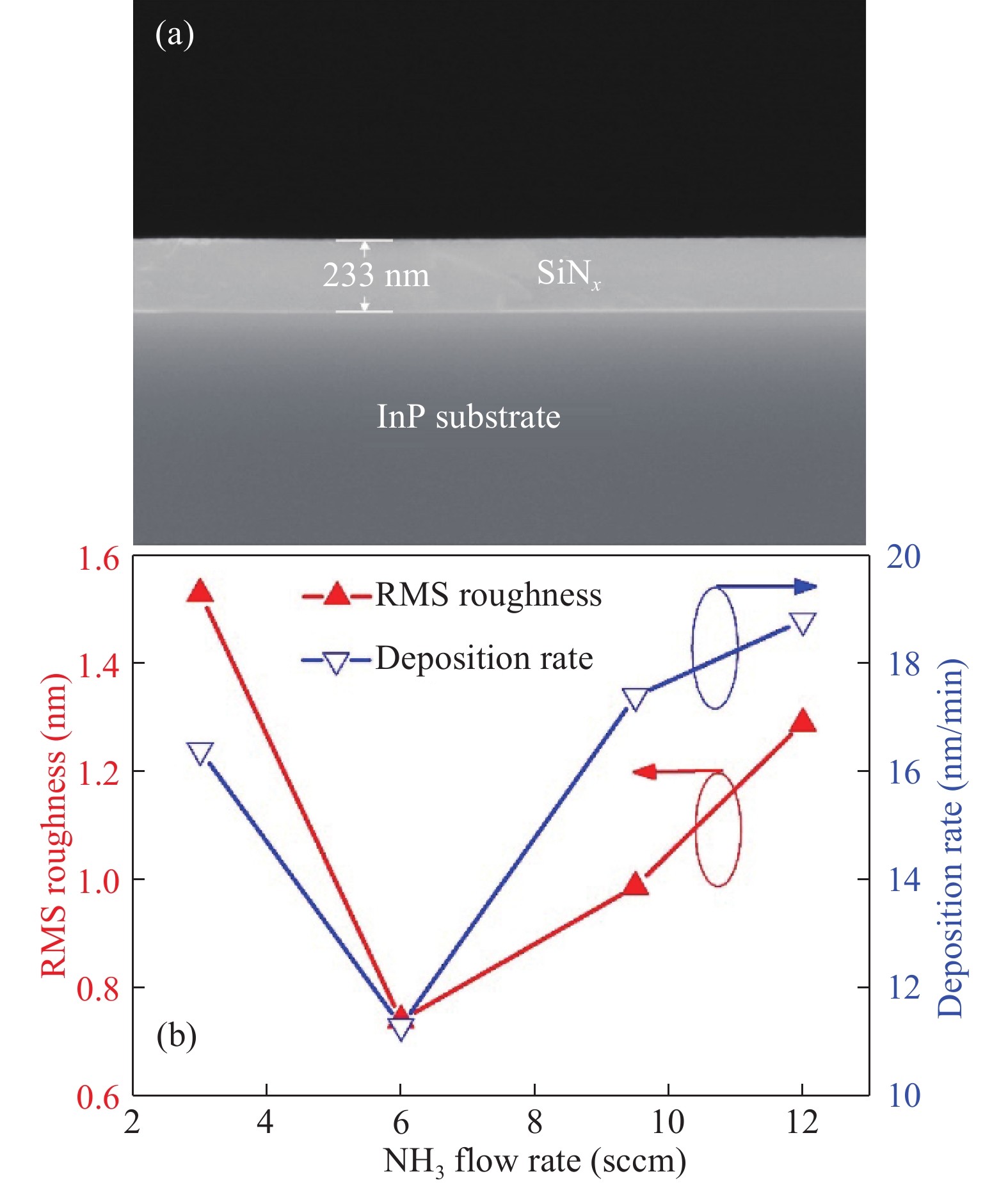
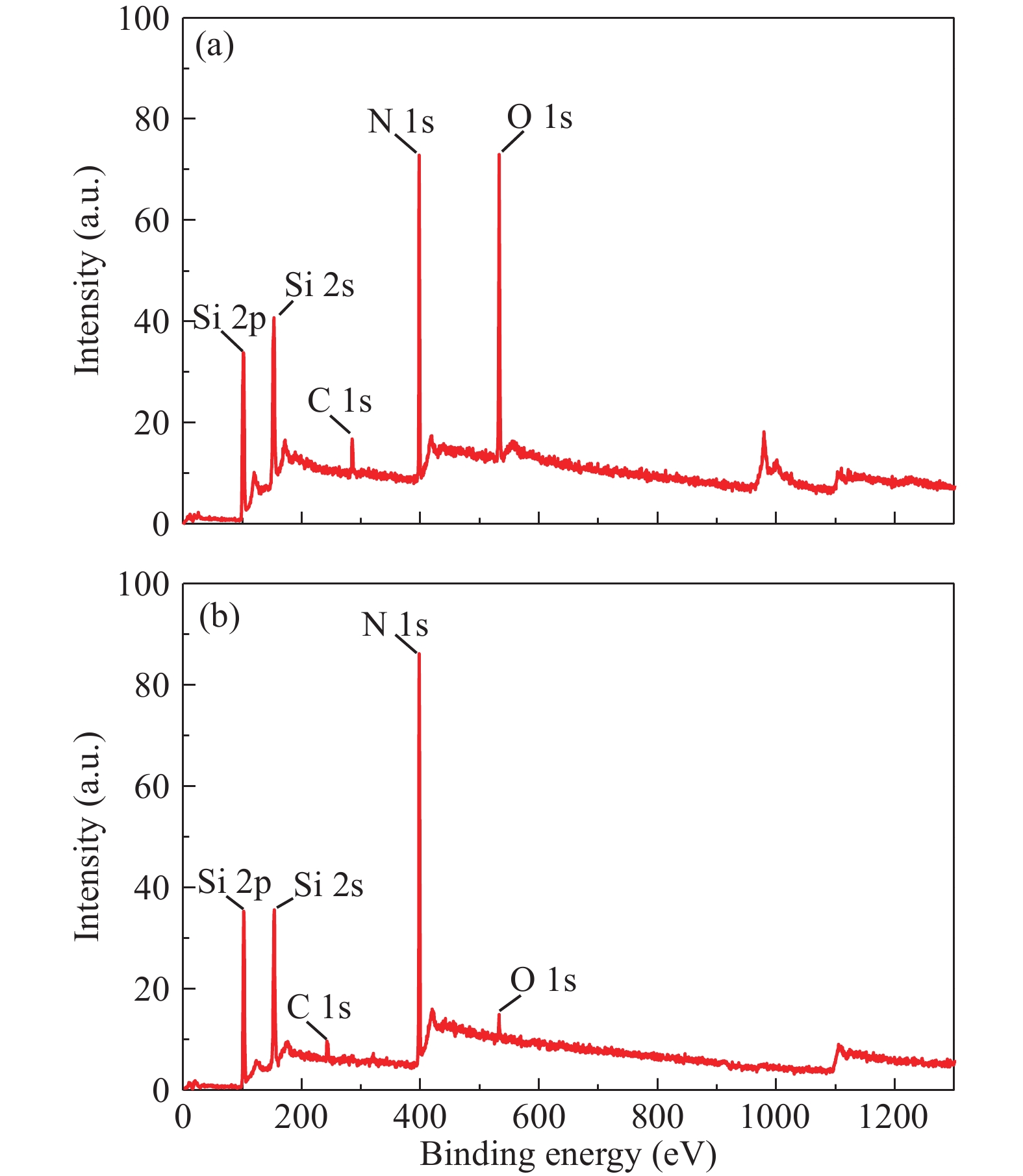
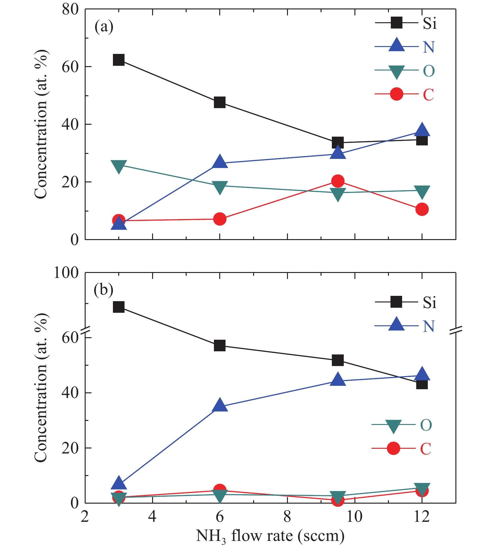
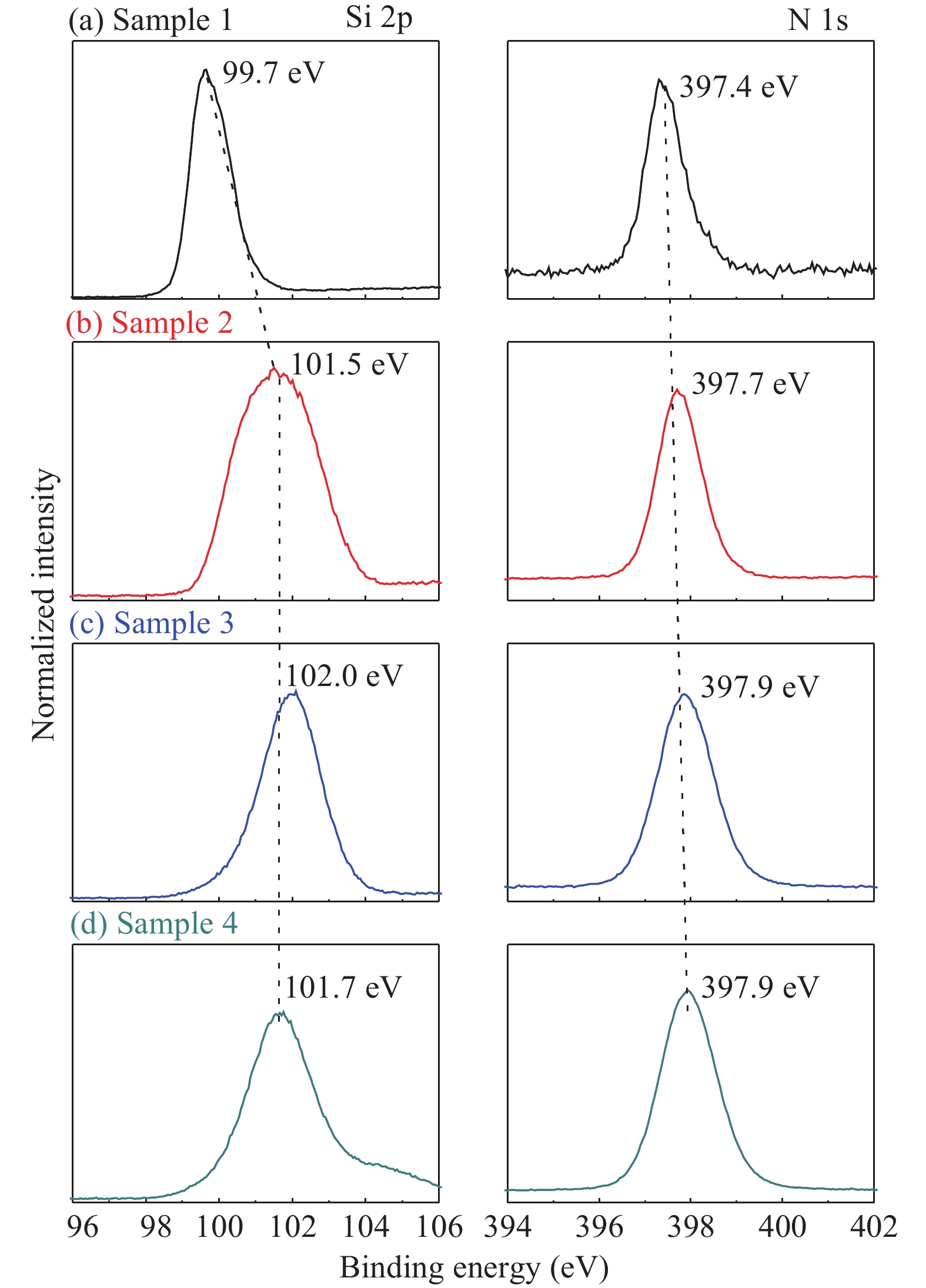
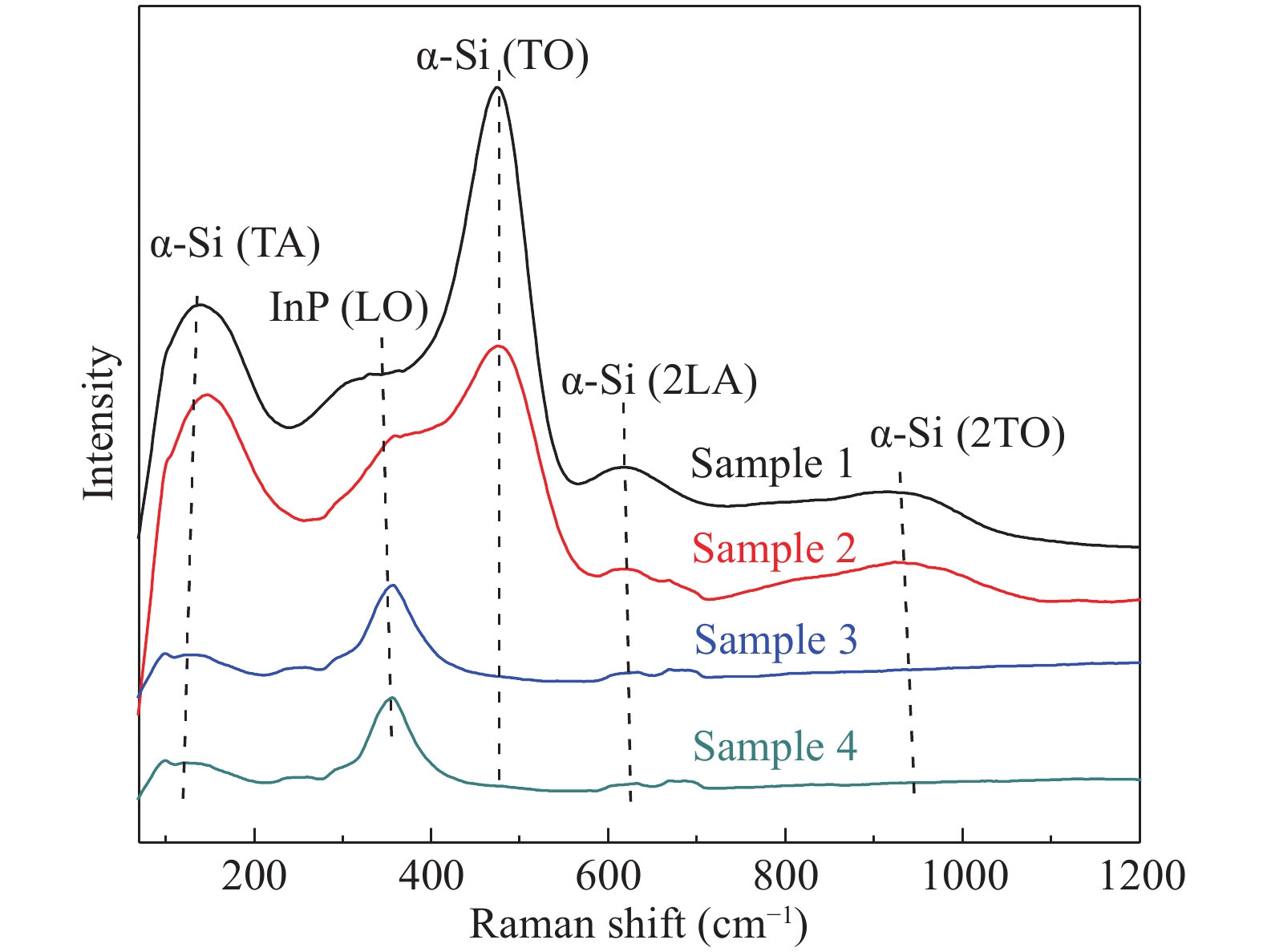
Table 1. The etching rate and Si/N ratio of SiNx samples with different NH3 flow rates.
| Sample No. | NH3 flow rate (sccm) | BOE etching rate (nm/min) | Si/N ratio |
| Sample 1 | 3.0 | 0 | 11.3 |
| Sample 2 | 6.0 | 10?20 | 1.5 |
| Sample 3 | 9.5 | 35 | 1.0 |
| Sample 4 | 12.0 | 230 | 0.9 |
 DownLoad: CSV
| [1] |
Yota J, Hander J, Saleh A A. A comparative study on inductively-coupled plasma high-density plasma, plasma-enhanced and low pressure chemical vapor deposition silicon nitride films. J Vac Sci Technol A, 2000, 18(2): 372 doi: 10.1116/1.582195
|
| [2] |
Lee S H, Lee I, Yi J. Silicon nitride films prepared by high-density plasma chemical vapor deposition for solar cell applications. Surf Coat Technol, 2002, 153(1): 67 doi: 10.1016/S0257-8972(01)01554-7
|
| [3] |
Medjdoub M, Courant J L, Maher H, et al. Inductively coupled plasma-plasma enhanced chemical vapor deposition silicon nitride for passivation of InP based high electron mobility transistors (HEMTs). Mater Sci Eng B, 2001, 80(1): 252
|
| [4] |
Zhang J, Umana-Membreno G A, Gu R, et al. Investigation of ICPECVD silicon nitride films for HgCdTe surface passivation. J Electron Mater, 2015, 44(9): 2990 doi: 10.1007/s11664-015-3703-y
|
| [5] |
Shi M, Shao X M, Tang H J, et al. Inductively coupled plasma chemical vapor deposition silicon nitride for passivation of In0.83Ga0.17As photodiodes. Infrared Phys Technol, 2014, 67: 197 doi: 10.1016/j.infrared.2014.06.003
|
| [6] |
Wei P, Li X, Li T, et al. Surface passivation of In0.83Ga0.17As photodiode with high-quality SiN layer fabricated by ICPCVD at the lower temperature. Infrared Phys Technol, 2014, 62: 13 doi: 10.1016/j.infrared.2013.10.003
|
| [7] |
Wang H, Ng G I, Yang H, et al. Ammonia (NH3) plasma surface passivation of InP/InGaAs heterojunction bipolar transistors. International Conference on Indium Phosphide and Related Materials, 2001: 421
|
| [8] |
Moriguchi H, Hoshi S, Ohshima T, et al. Isolation degradation of InAlAs/InGaAs/InP HEMTs due to bias stress depending on passivation films formed by PCVD. International Conference on Indium Phosphide and Related Materials, 2001: 417
|
| [9] |
Wang H, Ng G I, Yang H, et al. Understanding the degradation of InP/InGaAs heterojunction bipolar transistors induced by silicon nitride passivation. International Conference on Indium Phosphide and Related Materials, 2001: 252
|
| [10] |
Jin Z, Uchida K, Nozaki S, et al. Passivation of InP-based HBTs. Appl Surf Sci, 2006, 252(21): 7664 doi: 10.1016/j.apsusc.2006.03.050
|
| [11] |
Lee J W, Mackenzie K D, Johnson D, et al. Low temperature silicon nitride and silicon dioxide film processing by inductively coupled plasma chemical vapor deposition. J Electrochem Soc, 2000, 147(4): 1481 doi: 10.1149/1.1393382
|
| [12] |
Chou Y C, Lai R, Li G P, et al. Innovative nitride passivated pseudomorphic GaAs HEMTs. IEEE Electron Device Lett, 2003, 24(1): 7 doi: 10.1109/LED.2002.807313
|
| [13] |
Wolf R, Wandel K, Gruska B. Low-temperature ICPECVD of silicon nitride in SiH4-NH3-Ar discharges analyzed by spectroscopic ellipsometry and etch behavior in KOH and BHF. Surf Coat Technol, 2001, 142: 786
|
| [14] |
Shi M, Tang H J, Shao X M, et al. Interface property of silicon nitride films grown by inductively coupled plasma chemical vapor deposition and plasma enhanced chemical vapor deposition on In0.82Al0.18As. Infrared Phys Technol, 2015, 71: 384 doi: 10.1016/j.infrared.2015.04.011
|
| [15] |
Dekkers H F W, Wolf D S, Agostinelli G, et al. Requirements of PECVD SiNx:H layers for bulk passivation of mc-Si. Sol Energy Mater Sol Cells, 2006, 90(18): 3244
|
| [16] |
Knotter D M, Denteneer T J J. Etching mechanism of silicon nitride in HF-based solutions. J Electrochem Soc, 2001, 148(3): F43 doi: 10.1149/1.1348262
|
| [17] |
Karcher R, Ley L, Johnson R L. Electronic structure of hydrogenated and unhydrogenated amorphous SiNx (0 ≤ x ≤1.6): A photoemission study. Phys Rev B, 1984, 30(4): 1896 doi: 10.1103/PhysRevB.30.1896
|
| [18] |
Moulder J F, Stickle W F, Sobol P E, et al. Handbook of X-ray photoelectron spectroscopy. Eden Prairie: Physical Electronics, 1992
|
| [19] |
Korchagina T T, Marin D V, Volodin V A, et al. Structure and optical properties of SiNx:H films with Si nanoclusters produced by low-frequency plasma-enhanced chemical vapor deposition. Semiconductors, 2009, 43(11): 1514 doi: 10.1134/S1063782609110207
|
| [20] |
Wei W S, Xu G Y, Wang J L, et al. Raman spectra of intrinsic and doped hydrogenated nanocrystalline silicon films. Vacuum, 2007, 81(5): 656 doi: 10.1016/j.vacuum.2006.09.006
|


Article views: 7033 Times PDF downloads: 233 Times Cited by: 0 Times
Received: 16 November 2017 Revised: 12 January 2018 Online: Accepted Manuscript: 04 April 2018Uncorrected proof: 12 April 2018Published: 09 August 2018
| Citation: |
Yi Zhu, Xingyou Chen, Yingjie Ma, Yonggang Zhang, Ben Du, Yanhui Shi, Yi Gu. Surface and optical properties of silicon nitride deposited by inductively coupled plasma-chemical vapor deposition[J]. Journal of Semiconductors, 2018, 39(8): 083005. doi: 10.1088/1674-4926/39/8/083005
****
Y Zhu, X Y Chen, Y J Ma, Y G Zhang, B Du, Y H Shi, Y Gu, Surface and optical properties of silicon nitride deposited by inductively coupled plasma-chemical vapor deposition[J]. J. Semicond., 2018, 39(8): 083005. doi: 10.1088/1674-4926/39/8/083005.

|
Project supported by the National Key R&D Program of China (Nos. 2017YFB0405300, 2016YFB0402400) and the National Natural Science Foundation of China (Nos. 61775228, 61675225, 61605232).
| [1] |
Yota J, Hander J, Saleh A A. A comparative study on inductively-coupled plasma high-density plasma, plasma-enhanced and low pressure chemical vapor deposition silicon nitride films. J Vac Sci Technol A, 2000, 18(2): 372 doi: 10.1116/1.582195
|
| [2] |
Lee S H, Lee I, Yi J. Silicon nitride films prepared by high-density plasma chemical vapor deposition for solar cell applications. Surf Coat Technol, 2002, 153(1): 67 doi: 10.1016/S0257-8972(01)01554-7
|
| [3] |
Medjdoub M, Courant J L, Maher H, et al. Inductively coupled plasma-plasma enhanced chemical vapor deposition silicon nitride for passivation of InP based high electron mobility transistors (HEMTs). Mater Sci Eng B, 2001, 80(1): 252
|
| [4] |
Zhang J, Umana-Membreno G A, Gu R, et al. Investigation of ICPECVD silicon nitride films for HgCdTe surface passivation. J Electron Mater, 2015, 44(9): 2990 doi: 10.1007/s11664-015-3703-y
|
| [5] |
Shi M, Shao X M, Tang H J, et al. Inductively coupled plasma chemical vapor deposition silicon nitride for passivation of In0.83Ga0.17As photodiodes. Infrared Phys Technol, 2014, 67: 197 doi: 10.1016/j.infrared.2014.06.003
|
| [6] |
Wei P, Li X, Li T, et al. Surface passivation of In0.83Ga0.17As photodiode with high-quality SiN layer fabricated by ICPCVD at the lower temperature. Infrared Phys Technol, 2014, 62: 13 doi: 10.1016/j.infrared.2013.10.003
|
| [7] |
Wang H, Ng G I, Yang H, et al. Ammonia (NH3) plasma surface passivation of InP/InGaAs heterojunction bipolar transistors. International Conference on Indium Phosphide and Related Materials, 2001: 421
|
| [8] |
Moriguchi H, Hoshi S, Ohshima T, et al. Isolation degradation of InAlAs/InGaAs/InP HEMTs due to bias stress depending on passivation films formed by PCVD. International Conference on Indium Phosphide and Related Materials, 2001: 417
|
| [9] |
Wang H, Ng G I, Yang H, et al. Understanding the degradation of InP/InGaAs heterojunction bipolar transistors induced by silicon nitride passivation. International Conference on Indium Phosphide and Related Materials, 2001: 252
|
| [10] |
Jin Z, Uchida K, Nozaki S, et al. Passivation of InP-based HBTs. Appl Surf Sci, 2006, 252(21): 7664 doi: 10.1016/j.apsusc.2006.03.050
|
| [11] |
Lee J W, Mackenzie K D, Johnson D, et al. Low temperature silicon nitride and silicon dioxide film processing by inductively coupled plasma chemical vapor deposition. J Electrochem Soc, 2000, 147(4): 1481 doi: 10.1149/1.1393382
|
| [12] |
Chou Y C, Lai R, Li G P, et al. Innovative nitride passivated pseudomorphic GaAs HEMTs. IEEE Electron Device Lett, 2003, 24(1): 7 doi: 10.1109/LED.2002.807313
|
| [13] |
Wolf R, Wandel K, Gruska B. Low-temperature ICPECVD of silicon nitride in SiH4-NH3-Ar discharges analyzed by spectroscopic ellipsometry and etch behavior in KOH and BHF. Surf Coat Technol, 2001, 142: 786
|
| [14] |
Shi M, Tang H J, Shao X M, et al. Interface property of silicon nitride films grown by inductively coupled plasma chemical vapor deposition and plasma enhanced chemical vapor deposition on In0.82Al0.18As. Infrared Phys Technol, 2015, 71: 384 doi: 10.1016/j.infrared.2015.04.011
|
| [15] |
Dekkers H F W, Wolf D S, Agostinelli G, et al. Requirements of PECVD SiNx:H layers for bulk passivation of mc-Si. Sol Energy Mater Sol Cells, 2006, 90(18): 3244
|
| [16] |
Knotter D M, Denteneer T J J. Etching mechanism of silicon nitride in HF-based solutions. J Electrochem Soc, 2001, 148(3): F43 doi: 10.1149/1.1348262
|
| [17] |
Karcher R, Ley L, Johnson R L. Electronic structure of hydrogenated and unhydrogenated amorphous SiNx (0 ≤ x ≤1.6): A photoemission study. Phys Rev B, 1984, 30(4): 1896 doi: 10.1103/PhysRevB.30.1896
|
| [18] |
Moulder J F, Stickle W F, Sobol P E, et al. Handbook of X-ray photoelectron spectroscopy. Eden Prairie: Physical Electronics, 1992
|
| [19] |
Korchagina T T, Marin D V, Volodin V A, et al. Structure and optical properties of SiNx:H films with Si nanoclusters produced by low-frequency plasma-enhanced chemical vapor deposition. Semiconductors, 2009, 43(11): 1514 doi: 10.1134/S1063782609110207
|
| [20] |
Wei W S, Xu G Y, Wang J L, et al. Raman spectra of intrinsic and doped hydrogenated nanocrystalline silicon films. Vacuum, 2007, 81(5): 656 doi: 10.1016/j.vacuum.2006.09.006
|

 WeChat ID
Journal of Semiconductors © 2017 All Rights Reserved 京ICP備05085259號-2

