


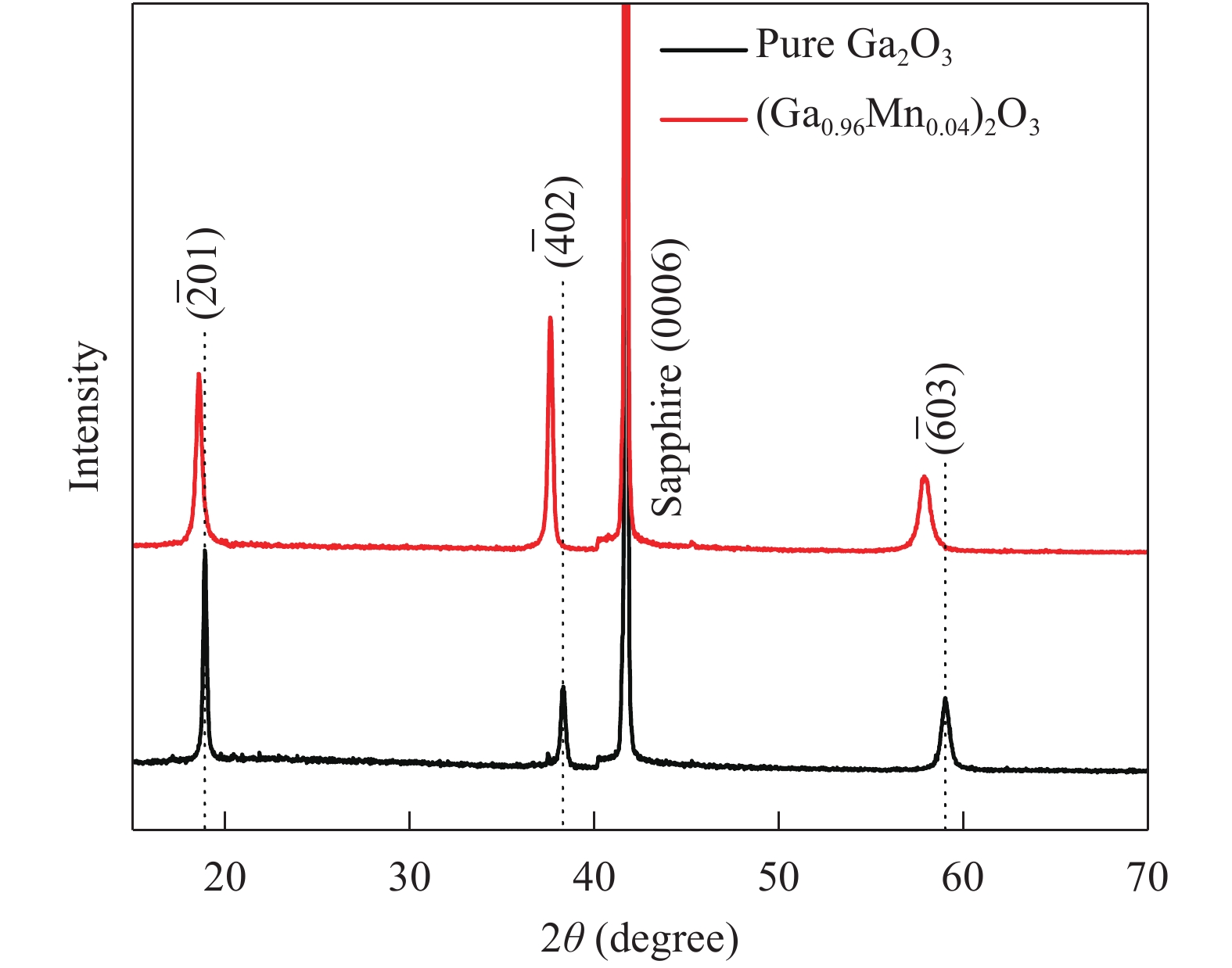
Fig. 1.
(Color online) X-ray diffraction θ–2θ scan of (Ga0.96Mn0.04)2O3 and pure Ga2O3 thin films.
SEMICONDUCTOR MATERIALS
Yuanqi Huang1, Zhengwei Chen1, 2, , Xiao Zhang1, 2, Xiaolong Wang1, Yusong Zhi1, Zhenping Wu1, 2 and Weihua Tang1, 2
Corresponding author: Zhengwei Chen, Email: zhengweichen@bupt.edu.cn
Abstract: High quality epitaxial single phase (Ga0.96Mn0.04)2O3 and Ga2O3 thin films have been prepared on sapphire substrates by using laser molecular beam epitaxy (L-MBE). X-ray diffraction results indicate that the thin films have the monoclinic structure with a
Key words: L-MBE, epitaxial growth, Mn doped Ga2O3 thin film, RT ferromagnetism
| [1] |
Wolf S A, Awschalom D D, Buhrman R A, et al. Spintronics: a spin-based electronics vision for the future. Science, 2001, 294(5546): 1488 doi: 10.1126/science.1065389
|
| [2] |
Fusil S, Garcia V, Barthélémy A, et al. Magneto electric devices for spintronics. Ann Rev Mater Res, 2014, 44: 91 doi: 10.1146/annurev-matsci-070813-113315
|
| [3] |
Suzuki R, Nakagomi S, Kokubun Y. Solar-blind photodiodes composed of an Au Schottky contact and a β-Ga2O3 single crystal with a high resistivity cap layer. Appl Phys Lett, 2011, 98(13): 131114 doi: 10.1063/1.3574911
|
| [4] |
Feng P, Zhang J Y, Li Q H, et al. Individual β-Ga2O3 nanowires as solar-blind photodetectors. Appl Phys Lett, 2006, 88(15): 153107 doi: 10.1063/1.2193463
|
| [5] |
Guo D Y, Wu Z P, Li P G, et al. Magnetic anisotropy and deep ultraviolet photoresponse characteristics in Ga2O3:Cr vermicular nanowire thin film nanostructure. RSC Adv, 2015, 5(17): 12894 doi: 10.1039/C4RA13813A
|
| [6] |
Ye S Y, Zhang Y H, He H L, et al. Simultaneous broadband near-infrared emission and magnetic properties of single phase Ni2+-doped β-Ga2O3 nanocrystals via mediated phase-controlled synthesis. J Mater Chem C, 2015, 3(12): 2886 doi: 10.1039/C4TC02624A
|
| [7] |
Chikoidze E, Bardeleben H J V, Akaiwa K, et al. Electrical, optical, and magnetic properties of Sn doped α-Ga2O3 thin films. J Appl Phys, 2016, 120(2): 025109 doi: 10.1063/1.4958860
|
| [8] |
Guo D Y, An Y H, Cui W, et al. Epitaxial growth and magnetic properties of ultraviolet transparent Ga2O3/(Ga1-xFex)2O3 multilayer thin films. Sci Rep, 2016, 6: 25166 doi: 10.1038/srep25166
|
| [9] |
Minami T, Shirai T, Nakatani T, et al. Electroluminescent devices with Ga2O3:Mn thin-film emitting layer prepared by sol-gel process. Jpn J Appl Phys, 2000, 39(6A): L524 doi: 10.1143/JJAP.39.L524
|
| [10] |
Minami T. Oxide thin-film electroluminescent devices and materials. Solid-State Electron, 2003, 47(12): 2237 doi: 10.1016/S0038-1101(03)00204-1
|
| [11] |
Kim J H, Yoon K H. Influence of post-deposition annealing on the microstructure and properties of Ga2O3:Mn thin films deposited by RF planar magnetron sputtering. J Mater Sci: Mater Electron, 2009, 20(9): 879 doi: 10.1007/s10854-008-9810-2
|
| [12] |
Hayashi H, Huang R, Ikeno H, et al. Room temperature ferromagnetism in Mn-doped γ-Ga2O3 with spinel structure. Appl Phys Lett, 2006, 89(18): 181903 doi: 10.1063/1.2369541
|
| [13] |
Hayashi H, Huang R, Oba F, et al. Site preference of cation vacancies in Mn-doped Ga2O3 with defective spinel structure. Appl Phys Lett, 2012, 101(24): 241906 doi: 10.1063/1.4770363
|
| [14] |
Guo D Y, Wu Z P, An Y H, et al. Room temperature ferromagnetism in (Ga1–xMnx)2O3 epitaxial thin films. J Mater Chem C, 2015, 3(8): 1830 doi: 10.1039/C4TC02833C
|
| [15] |
Guo D Y, Li P G, Wu Z P, et al. Inhibition of unintentional extra carriers by Mn valence change for high insulating devices. Sci Rep, 2016, 6: 24190 doi: 10.1038/srep24190
|
| [16] |
Dakhel A A. Structural, optical, and opto-dielectric properties of W-doped Ga2O3 thin films. J Mater Sci, 2012, 47(7): 3034 doi: 10.1007/s10853-011-6134-z
|
| [17] |
Guo D Y, Qian Y P, Su Y L, et al. Evidence for the bias-driven migration of oxygen vacancies in amorphous non-stoichiometric gallium oxide. AIP Adv, 2017, 7(6): 065312 doi: 10.1063/1.4990566
|
| [18] |
Guo D Y, Liu H, Li P G, et al. Zero-power-consumption solar-blind photodetector based on β-Ga2O3/NSTO heterojunction. ACS Appl Mater Interf, 2017, 9(2): 1619-1628 doi: 10.1021/acsami.6b13771
|
| [19] |
Guo D Y, Wu Z P, Li P G, et al. Fabrication of β-Ga2O3 thin films and solar-blind photodetectors by laser MBE technology. Opt Mater Express, 2014, 4(5): 1067 doi: 10.1364/OME.4.001067
|
| [20] |
An Y H, Zhi Y S, Cui W, et al. Thickness tuning photoelectric properties of β-Ga2O3 thin film base photodetectors. J Nanosci Nanotechnol, 2017, 17: 1 doi: 10.1166/jnn.2017.12932
|
| [21] |
Chen Z W, Saito K, Tanaka T, et al. Low temperature growth of europium doped Ga2O3 luminescent films. J Cryst Growth, 2015, 430: 28 doi: 10.1016/j.jcrysgro.2015.08.020
|
| [22] |
An Y K, Wang S Q, Duan L S, et al. Local Mn structure and room temperature ferromagnetism in Mn-doped In2O3 films. Appl Phys Lett, 2013, 102(21): 212411 doi: 10.1063/1.4808116
|
| [23] |
Kokubun Y, Miura K, Endo F, et al. Sol-gel prepared β-Ga2O3 thin films for ultraviolet photodetectors. Appl Phys Lett, 2007, 90(3): 031912 doi: 10.1063/1.2432946
|
| [24] |
Riesz F, Vignali C, Pelosi C, et al. An atomic force microscopy study of the surface morphology of InP/GaAs heteroepitaxial layers subjected to rapid thermal annealing. J Appl Phys, 1998, 83(1): 246 doi: 10.1063/1.366733
|
| [25] |
álvarez D, Hartwich J, Kretz J, et al. Scanning spreading resistance microscopy of fully depleted silicon-on-insulator devices. Microelectron Eng, 2003, 67(1): 945
|
| [26] |
Evarts E R, Cao L, Ricketts D S, et al. Spin transfer torque switching of magnetic tunnel junctions using a conductive atomic force microscope. Appl Phys Lett, 2009, 95(13): 132510 doi: 10.1063/1.3240884
|
| [27] |
Guo L J, Shen X P, Zhu G X, et al. Preparation and gas-sensing performance of In2O3 porous nanoplatelets. Sens Actuators B, 2011, 155(2): 752 doi: 10.1016/j.snb.2011.01.042
|
| [28] |
Kumar S S, Rubio E J, Nooraalam M, et al. Structure, morphology, and optical properties of amorphous and nanocrystalline gallium oxide thin films. J Phys Chem C, 2013, 117(8): 4194 doi: 10.1021/jp311300e
|
| [29] |
Giri P K. Structural, optical and magnetic properties of Ni doped ZnO nanoparticles: correlation of magnetic moment with defect density. Appl Surf Sci, 2015, 356: 804 doi: 10.1016/j.apsusc.2015.08.163
|
| [30] |
Chen Y, Wu B, Yuan H K, et al. The defect-induced changes of the electronic and magnetic properties in the inverse Heusler alloy Ti2CoAl. J Solid State Chem, 2015, 221(221): 311 doi: 10.1016/j.jssc.2014.08.027
|
| [31] |
Murugan R, Vijayaprasath G, Mahalingam T, et al. Defect induced magnetic transition in Co doped CeO2, sputtered thin films. Ceram Int, 2016, 42(10): 11724 doi: 10.1016/j.ceramint.2016.04.091
|
| [32] |
Pei G Q, Xia C T, Dong Y J, et al. Studies of magnetic interactions in Mn-doped β-Ga2O3 from first-principles calculations. Scripta Materialia, 2008, 58(11): 943 doi: 10.1016/j.scriptamat.2008.01.059
|
| [33] |
Lovejoy T C, Chen R, Yitamben E N, et al. Incorporation, valence state, and electronic structure of Mn and Cr in bulk single crystal β-Ga2O3. J Appl Phys, 2012, 111(12): 123716 doi: 10.1063/1.4729289
|
| [34] |
Wang G F, Li Y J, Zhong D X, et al. Study of effects of heavy Mn doping on electronic structure and optical property of β-Ga2O3 with the first principle. Journal of Zhejiang Sci-Tech University, 2014, 31(5): 586
|
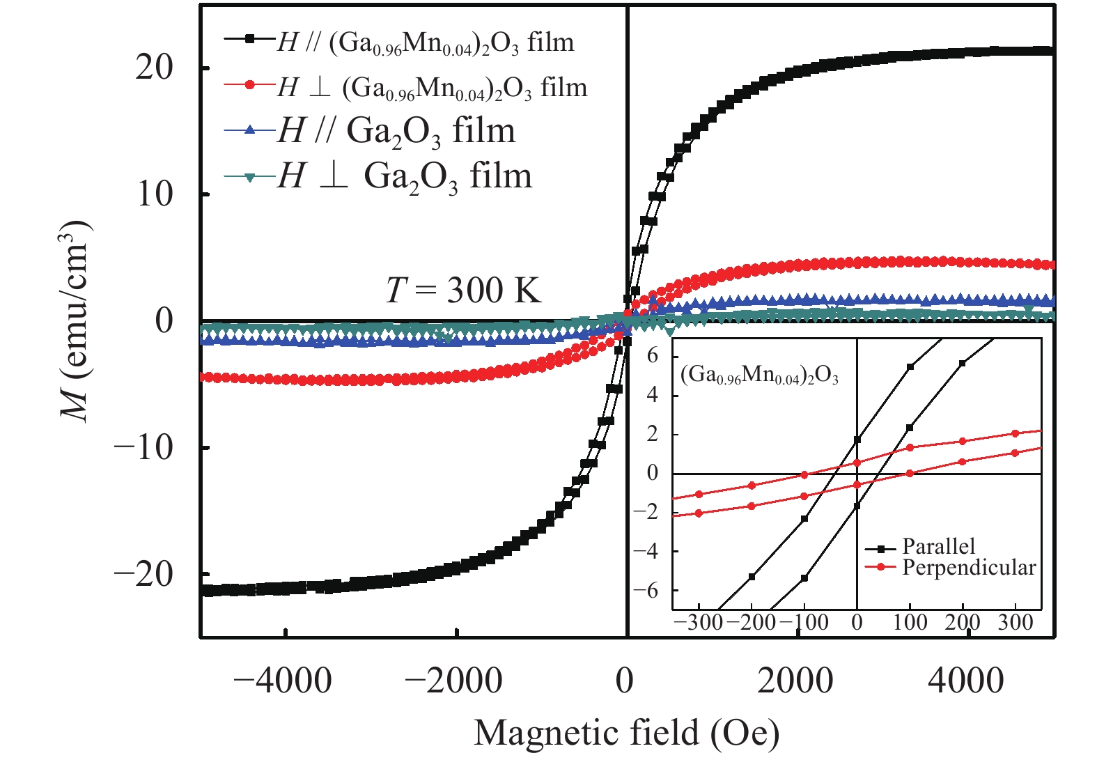
Table 1. The magnetic parameters of β-(Ga0.96Mn0.04)2O3 thin film.
| Magnetic field
direction |
Magnetic moments (μB/Mn) | Mr (emu/cm3) |
Coercivity
(Oe) |
| Parallel | 0.76 | 1.69 | 42.07 |
| Perpendicular | 0.17 | 0.52 | 91.36 |
 DownLoad: CSV
| [1] |
Wolf S A, Awschalom D D, Buhrman R A, et al. Spintronics: a spin-based electronics vision for the future. Science, 2001, 294(5546): 1488 doi: 10.1126/science.1065389
|
| [2] |
Fusil S, Garcia V, Barthélémy A, et al. Magneto electric devices for spintronics. Ann Rev Mater Res, 2014, 44: 91 doi: 10.1146/annurev-matsci-070813-113315
|
| [3] |
Suzuki R, Nakagomi S, Kokubun Y. Solar-blind photodiodes composed of an Au Schottky contact and a β-Ga2O3 single crystal with a high resistivity cap layer. Appl Phys Lett, 2011, 98(13): 131114 doi: 10.1063/1.3574911
|
| [4] |
Feng P, Zhang J Y, Li Q H, et al. Individual β-Ga2O3 nanowires as solar-blind photodetectors. Appl Phys Lett, 2006, 88(15): 153107 doi: 10.1063/1.2193463
|
| [5] |
Guo D Y, Wu Z P, Li P G, et al. Magnetic anisotropy and deep ultraviolet photoresponse characteristics in Ga2O3:Cr vermicular nanowire thin film nanostructure. RSC Adv, 2015, 5(17): 12894 doi: 10.1039/C4RA13813A
|
| [6] |
Ye S Y, Zhang Y H, He H L, et al. Simultaneous broadband near-infrared emission and magnetic properties of single phase Ni2+-doped β-Ga2O3 nanocrystals via mediated phase-controlled synthesis. J Mater Chem C, 2015, 3(12): 2886 doi: 10.1039/C4TC02624A
|
| [7] |
Chikoidze E, Bardeleben H J V, Akaiwa K, et al. Electrical, optical, and magnetic properties of Sn doped α-Ga2O3 thin films. J Appl Phys, 2016, 120(2): 025109 doi: 10.1063/1.4958860
|
| [8] |
Guo D Y, An Y H, Cui W, et al. Epitaxial growth and magnetic properties of ultraviolet transparent Ga2O3/(Ga1-xFex)2O3 multilayer thin films. Sci Rep, 2016, 6: 25166 doi: 10.1038/srep25166
|
| [9] |
Minami T, Shirai T, Nakatani T, et al. Electroluminescent devices with Ga2O3:Mn thin-film emitting layer prepared by sol-gel process. Jpn J Appl Phys, 2000, 39(6A): L524 doi: 10.1143/JJAP.39.L524
|
| [10] |
Minami T. Oxide thin-film electroluminescent devices and materials. Solid-State Electron, 2003, 47(12): 2237 doi: 10.1016/S0038-1101(03)00204-1
|
| [11] |
Kim J H, Yoon K H. Influence of post-deposition annealing on the microstructure and properties of Ga2O3:Mn thin films deposited by RF planar magnetron sputtering. J Mater Sci: Mater Electron, 2009, 20(9): 879 doi: 10.1007/s10854-008-9810-2
|
| [12] |
Hayashi H, Huang R, Ikeno H, et al. Room temperature ferromagnetism in Mn-doped γ-Ga2O3 with spinel structure. Appl Phys Lett, 2006, 89(18): 181903 doi: 10.1063/1.2369541
|
| [13] |
Hayashi H, Huang R, Oba F, et al. Site preference of cation vacancies in Mn-doped Ga2O3 with defective spinel structure. Appl Phys Lett, 2012, 101(24): 241906 doi: 10.1063/1.4770363
|
| [14] |
Guo D Y, Wu Z P, An Y H, et al. Room temperature ferromagnetism in (Ga1–xMnx)2O3 epitaxial thin films. J Mater Chem C, 2015, 3(8): 1830 doi: 10.1039/C4TC02833C
|
| [15] |
Guo D Y, Li P G, Wu Z P, et al. Inhibition of unintentional extra carriers by Mn valence change for high insulating devices. Sci Rep, 2016, 6: 24190 doi: 10.1038/srep24190
|
| [16] |
Dakhel A A. Structural, optical, and opto-dielectric properties of W-doped Ga2O3 thin films. J Mater Sci, 2012, 47(7): 3034 doi: 10.1007/s10853-011-6134-z
|
| [17] |
Guo D Y, Qian Y P, Su Y L, et al. Evidence for the bias-driven migration of oxygen vacancies in amorphous non-stoichiometric gallium oxide. AIP Adv, 2017, 7(6): 065312 doi: 10.1063/1.4990566
|
| [18] |
Guo D Y, Liu H, Li P G, et al. Zero-power-consumption solar-blind photodetector based on β-Ga2O3/NSTO heterojunction. ACS Appl Mater Interf, 2017, 9(2): 1619-1628 doi: 10.1021/acsami.6b13771
|
| [19] |
Guo D Y, Wu Z P, Li P G, et al. Fabrication of β-Ga2O3 thin films and solar-blind photodetectors by laser MBE technology. Opt Mater Express, 2014, 4(5): 1067 doi: 10.1364/OME.4.001067
|
| [20] |
An Y H, Zhi Y S, Cui W, et al. Thickness tuning photoelectric properties of β-Ga2O3 thin film base photodetectors. J Nanosci Nanotechnol, 2017, 17: 1 doi: 10.1166/jnn.2017.12932
|
| [21] |
Chen Z W, Saito K, Tanaka T, et al. Low temperature growth of europium doped Ga2O3 luminescent films. J Cryst Growth, 2015, 430: 28 doi: 10.1016/j.jcrysgro.2015.08.020
|
| [22] |
An Y K, Wang S Q, Duan L S, et al. Local Mn structure and room temperature ferromagnetism in Mn-doped In2O3 films. Appl Phys Lett, 2013, 102(21): 212411 doi: 10.1063/1.4808116
|
| [23] |
Kokubun Y, Miura K, Endo F, et al. Sol-gel prepared β-Ga2O3 thin films for ultraviolet photodetectors. Appl Phys Lett, 2007, 90(3): 031912 doi: 10.1063/1.2432946
|
| [24] |
Riesz F, Vignali C, Pelosi C, et al. An atomic force microscopy study of the surface morphology of InP/GaAs heteroepitaxial layers subjected to rapid thermal annealing. J Appl Phys, 1998, 83(1): 246 doi: 10.1063/1.366733
|
| [25] |
álvarez D, Hartwich J, Kretz J, et al. Scanning spreading resistance microscopy of fully depleted silicon-on-insulator devices. Microelectron Eng, 2003, 67(1): 945
|
| [26] |
Evarts E R, Cao L, Ricketts D S, et al. Spin transfer torque switching of magnetic tunnel junctions using a conductive atomic force microscope. Appl Phys Lett, 2009, 95(13): 132510 doi: 10.1063/1.3240884
|
| [27] |
Guo L J, Shen X P, Zhu G X, et al. Preparation and gas-sensing performance of In2O3 porous nanoplatelets. Sens Actuators B, 2011, 155(2): 752 doi: 10.1016/j.snb.2011.01.042
|
| [28] |
Kumar S S, Rubio E J, Nooraalam M, et al. Structure, morphology, and optical properties of amorphous and nanocrystalline gallium oxide thin films. J Phys Chem C, 2013, 117(8): 4194 doi: 10.1021/jp311300e
|
| [29] |
Giri P K. Structural, optical and magnetic properties of Ni doped ZnO nanoparticles: correlation of magnetic moment with defect density. Appl Surf Sci, 2015, 356: 804 doi: 10.1016/j.apsusc.2015.08.163
|
| [30] |
Chen Y, Wu B, Yuan H K, et al. The defect-induced changes of the electronic and magnetic properties in the inverse Heusler alloy Ti2CoAl. J Solid State Chem, 2015, 221(221): 311 doi: 10.1016/j.jssc.2014.08.027
|
| [31] |
Murugan R, Vijayaprasath G, Mahalingam T, et al. Defect induced magnetic transition in Co doped CeO2, sputtered thin films. Ceram Int, 2016, 42(10): 11724 doi: 10.1016/j.ceramint.2016.04.091
|
| [32] |
Pei G Q, Xia C T, Dong Y J, et al. Studies of magnetic interactions in Mn-doped β-Ga2O3 from first-principles calculations. Scripta Materialia, 2008, 58(11): 943 doi: 10.1016/j.scriptamat.2008.01.059
|
| [33] |
Lovejoy T C, Chen R, Yitamben E N, et al. Incorporation, valence state, and electronic structure of Mn and Cr in bulk single crystal β-Ga2O3. J Appl Phys, 2012, 111(12): 123716 doi: 10.1063/1.4729289
|
| [34] |
Wang G F, Li Y J, Zhong D X, et al. Study of effects of heavy Mn doping on electronic structure and optical property of β-Ga2O3 with the first principle. Journal of Zhejiang Sci-Tech University, 2014, 31(5): 586
|


Article views: 4346 Times PDF downloads: 64 Times Cited by: 0 Times
Received: 20 August 2017 Revised: 15 December 2017 Online: Uncorrected proof: 24 January 2018Accepted Manuscript: 18 April 2018Published: 01 May 2018
| Citation: |
Yuanqi Huang, Zhengwei Chen, Xiao Zhang, Xiaolong Wang, Yusong Zhi, Zhenping Wu, Weihua Tang. The structure and magnetic properties of β-(Ga0.96Mn0.04)2O3 thin film[J]. Journal of Semiconductors, 2018, 39(5): 053002. doi: 10.1088/1674-4926/39/5/053002
****
Y Q Huang, Z W Chen, X Zhang, X L Wang, Y S Zhi, Z P Wu, W H Tang. The structure and magnetic properties of β-(Ga0.96Mn0.04)2O3 thin film[J]. J. Semicond., 2018, 39(5): 053002. doi: 10.1088/1674-4926/39/5/053002.

|
Project supported by the National Natural Science Foundation of China (Nos. 11404029, 51572033, 51172208) and the Fund of State Key Laboratory of Information Photonics and Optical Communications (BUPT).
| [1] |
Wolf S A, Awschalom D D, Buhrman R A, et al. Spintronics: a spin-based electronics vision for the future. Science, 2001, 294(5546): 1488 doi: 10.1126/science.1065389
|
| [2] |
Fusil S, Garcia V, Barthélémy A, et al. Magneto electric devices for spintronics. Ann Rev Mater Res, 2014, 44: 91 doi: 10.1146/annurev-matsci-070813-113315
|
| [3] |
Suzuki R, Nakagomi S, Kokubun Y. Solar-blind photodiodes composed of an Au Schottky contact and a β-Ga2O3 single crystal with a high resistivity cap layer. Appl Phys Lett, 2011, 98(13): 131114 doi: 10.1063/1.3574911
|
| [4] |
Feng P, Zhang J Y, Li Q H, et al. Individual β-Ga2O3 nanowires as solar-blind photodetectors. Appl Phys Lett, 2006, 88(15): 153107 doi: 10.1063/1.2193463
|
| [5] |
Guo D Y, Wu Z P, Li P G, et al. Magnetic anisotropy and deep ultraviolet photoresponse characteristics in Ga2O3:Cr vermicular nanowire thin film nanostructure. RSC Adv, 2015, 5(17): 12894 doi: 10.1039/C4RA13813A
|
| [6] |
Ye S Y, Zhang Y H, He H L, et al. Simultaneous broadband near-infrared emission and magnetic properties of single phase Ni2+-doped β-Ga2O3 nanocrystals via mediated phase-controlled synthesis. J Mater Chem C, 2015, 3(12): 2886 doi: 10.1039/C4TC02624A
|
| [7] |
Chikoidze E, Bardeleben H J V, Akaiwa K, et al. Electrical, optical, and magnetic properties of Sn doped α-Ga2O3 thin films. J Appl Phys, 2016, 120(2): 025109 doi: 10.1063/1.4958860
|
| [8] |
Guo D Y, An Y H, Cui W, et al. Epitaxial growth and magnetic properties of ultraviolet transparent Ga2O3/(Ga1-xFex)2O3 multilayer thin films. Sci Rep, 2016, 6: 25166 doi: 10.1038/srep25166
|
| [9] |
Minami T, Shirai T, Nakatani T, et al. Electroluminescent devices with Ga2O3:Mn thin-film emitting layer prepared by sol-gel process. Jpn J Appl Phys, 2000, 39(6A): L524 doi: 10.1143/JJAP.39.L524
|
| [10] |
Minami T. Oxide thin-film electroluminescent devices and materials. Solid-State Electron, 2003, 47(12): 2237 doi: 10.1016/S0038-1101(03)00204-1
|
| [11] |
Kim J H, Yoon K H. Influence of post-deposition annealing on the microstructure and properties of Ga2O3:Mn thin films deposited by RF planar magnetron sputtering. J Mater Sci: Mater Electron, 2009, 20(9): 879 doi: 10.1007/s10854-008-9810-2
|
| [12] |
Hayashi H, Huang R, Ikeno H, et al. Room temperature ferromagnetism in Mn-doped γ-Ga2O3 with spinel structure. Appl Phys Lett, 2006, 89(18): 181903 doi: 10.1063/1.2369541
|
| [13] |
Hayashi H, Huang R, Oba F, et al. Site preference of cation vacancies in Mn-doped Ga2O3 with defective spinel structure. Appl Phys Lett, 2012, 101(24): 241906 doi: 10.1063/1.4770363
|
| [14] |
Guo D Y, Wu Z P, An Y H, et al. Room temperature ferromagnetism in (Ga1–xMnx)2O3 epitaxial thin films. J Mater Chem C, 2015, 3(8): 1830 doi: 10.1039/C4TC02833C
|
| [15] |
Guo D Y, Li P G, Wu Z P, et al. Inhibition of unintentional extra carriers by Mn valence change for high insulating devices. Sci Rep, 2016, 6: 24190 doi: 10.1038/srep24190
|
| [16] |
Dakhel A A. Structural, optical, and opto-dielectric properties of W-doped Ga2O3 thin films. J Mater Sci, 2012, 47(7): 3034 doi: 10.1007/s10853-011-6134-z
|
| [17] |
Guo D Y, Qian Y P, Su Y L, et al. Evidence for the bias-driven migration of oxygen vacancies in amorphous non-stoichiometric gallium oxide. AIP Adv, 2017, 7(6): 065312 doi: 10.1063/1.4990566
|
| [18] |
Guo D Y, Liu H, Li P G, et al. Zero-power-consumption solar-blind photodetector based on β-Ga2O3/NSTO heterojunction. ACS Appl Mater Interf, 2017, 9(2): 1619-1628 doi: 10.1021/acsami.6b13771
|
| [19] |
Guo D Y, Wu Z P, Li P G, et al. Fabrication of β-Ga2O3 thin films and solar-blind photodetectors by laser MBE technology. Opt Mater Express, 2014, 4(5): 1067 doi: 10.1364/OME.4.001067
|
| [20] |
An Y H, Zhi Y S, Cui W, et al. Thickness tuning photoelectric properties of β-Ga2O3 thin film base photodetectors. J Nanosci Nanotechnol, 2017, 17: 1 doi: 10.1166/jnn.2017.12932
|
| [21] |
Chen Z W, Saito K, Tanaka T, et al. Low temperature growth of europium doped Ga2O3 luminescent films. J Cryst Growth, 2015, 430: 28 doi: 10.1016/j.jcrysgro.2015.08.020
|
| [22] |
An Y K, Wang S Q, Duan L S, et al. Local Mn structure and room temperature ferromagnetism in Mn-doped In2O3 films. Appl Phys Lett, 2013, 102(21): 212411 doi: 10.1063/1.4808116
|
| [23] |
Kokubun Y, Miura K, Endo F, et al. Sol-gel prepared β-Ga2O3 thin films for ultraviolet photodetectors. Appl Phys Lett, 2007, 90(3): 031912 doi: 10.1063/1.2432946
|
| [24] |
Riesz F, Vignali C, Pelosi C, et al. An atomic force microscopy study of the surface morphology of InP/GaAs heteroepitaxial layers subjected to rapid thermal annealing. J Appl Phys, 1998, 83(1): 246 doi: 10.1063/1.366733
|
| [25] |
álvarez D, Hartwich J, Kretz J, et al. Scanning spreading resistance microscopy of fully depleted silicon-on-insulator devices. Microelectron Eng, 2003, 67(1): 945
|
| [26] |
Evarts E R, Cao L, Ricketts D S, et al. Spin transfer torque switching of magnetic tunnel junctions using a conductive atomic force microscope. Appl Phys Lett, 2009, 95(13): 132510 doi: 10.1063/1.3240884
|
| [27] |
Guo L J, Shen X P, Zhu G X, et al. Preparation and gas-sensing performance of In2O3 porous nanoplatelets. Sens Actuators B, 2011, 155(2): 752 doi: 10.1016/j.snb.2011.01.042
|
| [28] |
Kumar S S, Rubio E J, Nooraalam M, et al. Structure, morphology, and optical properties of amorphous and nanocrystalline gallium oxide thin films. J Phys Chem C, 2013, 117(8): 4194 doi: 10.1021/jp311300e
|
| [29] |
Giri P K. Structural, optical and magnetic properties of Ni doped ZnO nanoparticles: correlation of magnetic moment with defect density. Appl Surf Sci, 2015, 356: 804 doi: 10.1016/j.apsusc.2015.08.163
|
| [30] |
Chen Y, Wu B, Yuan H K, et al. The defect-induced changes of the electronic and magnetic properties in the inverse Heusler alloy Ti2CoAl. J Solid State Chem, 2015, 221(221): 311 doi: 10.1016/j.jssc.2014.08.027
|
| [31] |
Murugan R, Vijayaprasath G, Mahalingam T, et al. Defect induced magnetic transition in Co doped CeO2, sputtered thin films. Ceram Int, 2016, 42(10): 11724 doi: 10.1016/j.ceramint.2016.04.091
|
| [32] |
Pei G Q, Xia C T, Dong Y J, et al. Studies of magnetic interactions in Mn-doped β-Ga2O3 from first-principles calculations. Scripta Materialia, 2008, 58(11): 943 doi: 10.1016/j.scriptamat.2008.01.059
|
| [33] |
Lovejoy T C, Chen R, Yitamben E N, et al. Incorporation, valence state, and electronic structure of Mn and Cr in bulk single crystal β-Ga2O3. J Appl Phys, 2012, 111(12): 123716 doi: 10.1063/1.4729289
|
| [34] |
Wang G F, Li Y J, Zhong D X, et al. Study of effects of heavy Mn doping on electronic structure and optical property of β-Ga2O3 with the first principle. Journal of Zhejiang Sci-Tech University, 2014, 31(5): 586
|

 WeChat ID
Journal of Semiconductors © 2017 All Rights Reserved 京ICP備05085259號(hào)-2

