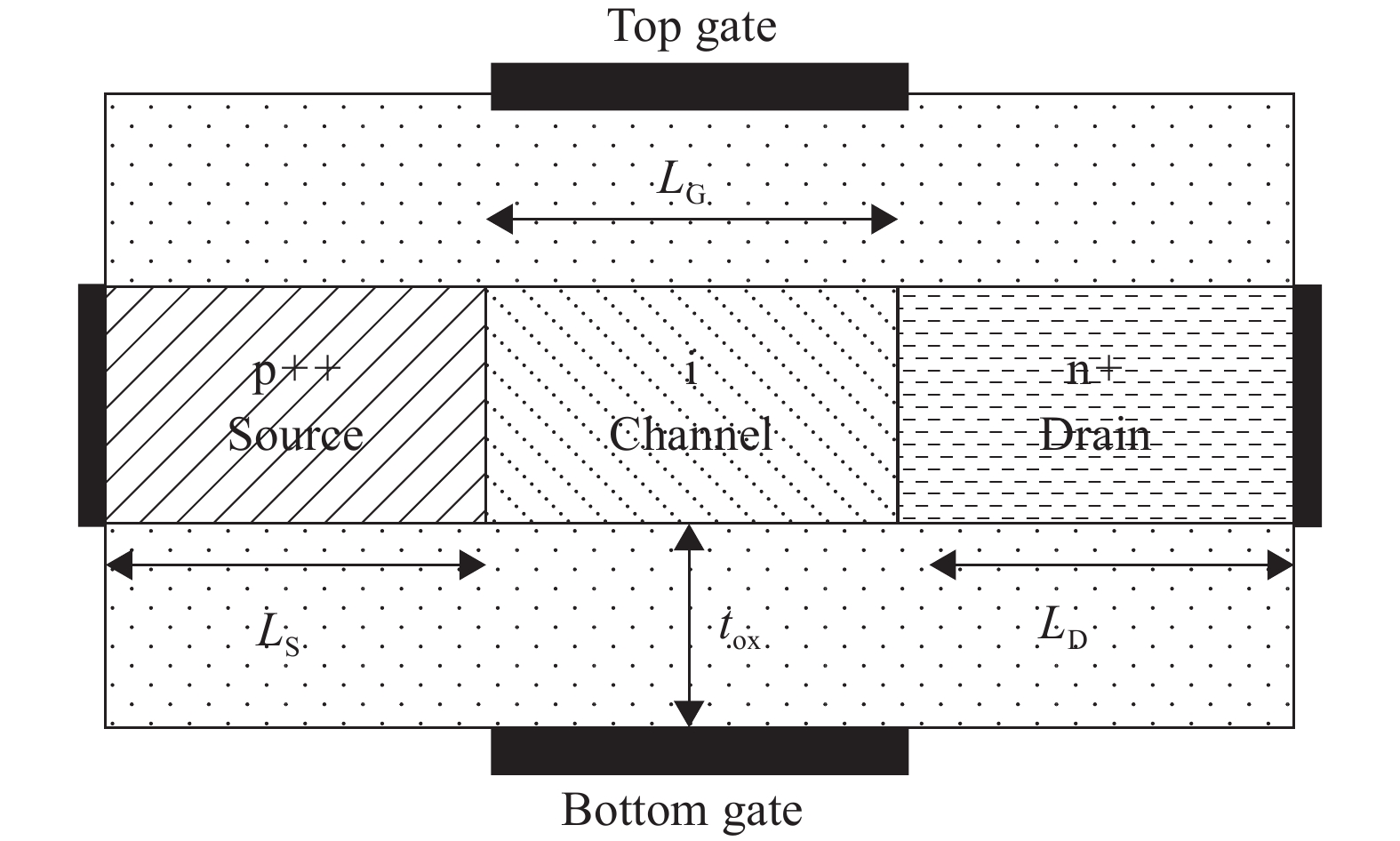
Fig. 1.
Schematic diagram for DG tunnel FET with high-k dielectric.
SEMICONDUCTOR DEVICES
Corresponding author: Shashi Bala, Email: shashi.sbbs@gmail.com
Abstract: A double-gate tunnel field-effect transistor (DG tunnel FET) has been designed and investigated for various channel materials such as silicon (Si), gallium arsenide (GaAs), alminium gallium arsenide (AlxGa1?xAs) and CNT using a nano ViDES Device and TCAD SILVACO ATLAS simulator. The proposed devices are compared on the basis of inverse subthreshold slope (SS), ION/IOFF current ratio and leakage current. Using Si as the channel material limits the property to reduce leakage current with scaling of channel, whereas the AlxGa1?xAs based DG tunnel FET provides a better ION/IOFF current ratio (2.51 × 10⁶) as compared to other devices keeping the leakage current within permissible limits. The performed silmulation of the CNT based channel in the double-gate tunnel field-effect transistor using the nano ViDES shows better performace for a sub-threshold slope of 29.4 mV/dec as the channel is scaled down. The proposed work shows the potential of the CNT channel based DG tunnel FET as a futuristic device for better switching and high retention time, which makes it suitable for memory based circuits.
Key words: band-to-band tunneling (BTBT), double gate (DG), silicon (Si), gallium arsenide (GaAs), aluminum gallium arsenide (AlxGa1?xAs), tunnel field effect transistor (FET), carbon nanotube (CNT)
| [1] |
Sakurai T. Perspectives of low-power VLSI's. IEICE trans Electron, 2004, 87(4): 429
|
| [2] |
Bernstein K, Cavin R K, Porod W, et al. Device and architecture outlook for beyond CMOS switches. Proc IEEE, 2010, 98(12): 2169 doi: 10.1109/JPROC.2010.2066530
|
| [3] |
Seabaugh A C, Zhang Q. Low-voltage tunnel transistors for beyond CMOS logic. Proc IEEE, 2010, 98(12): 2095 doi: 10.1109/JPROC.2010.2070470
|
| [4] |
Zener C. A theory of the electrical breakdown of solid dielectrics. Proc Royal Soc London A, 1934, 145(855): 523 doi: 10.1098/rspa.1934.0116
|
| [5] |
Silvaco ATLAS device simulator and user manual, silvaco int; Santa Clara, CA, USA 5.19.2 2013
|
| [6] |
Appenzeller J, Lin Y M, Knoch J, et al. Comparing carbon nanotube transistors-the ideal choice: a novel tunneling device design. IEEE Trans Electron Devices, 2005, 52(12): 2568 doi: 10.1109/TED.2005.859654
|
| [7] |
Sharma S K, Raj B, Khosla M. Comparative analysis of MOSFET, CNTFET and NWFET for energy efficient VLSI circuit design. J VLSI Des Tools Technol, 2016, 6: 1
|
| [8] |
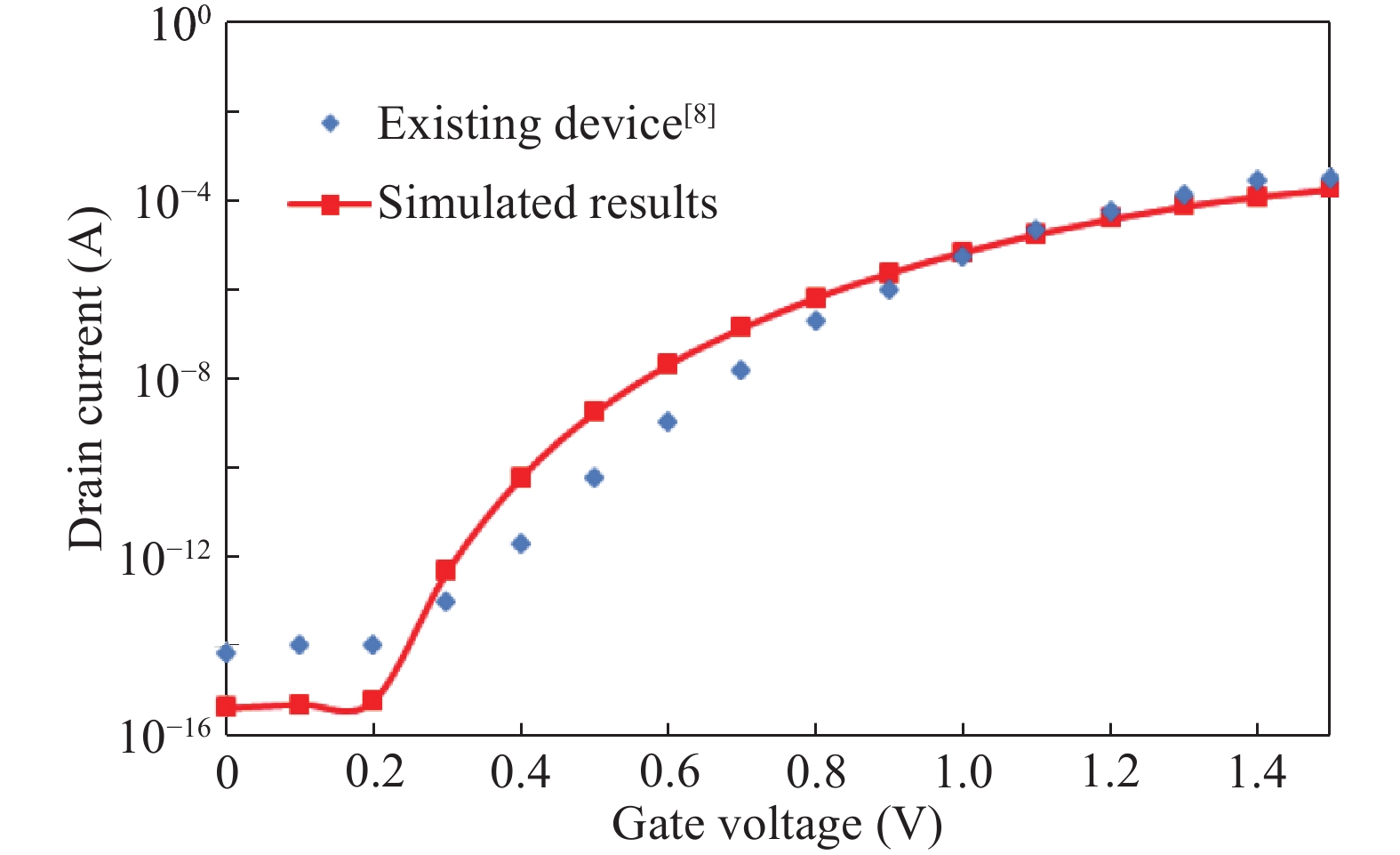
Boucart K, Ionescu A M. Length scaling of the double gate tunnel FET with a high-k gate dielectric. Solid-State Electron, 2007, 51(11): 1500
|
| [9] |
Sharma S K, Raj B, Khosla M. A Gaussian approach for analytical subthreshold current model of cylindrical nanowire FET with quantum mechanical effects. Microelectron J, 2016, 53: 65 doi: 10.1016/j.mejo.2016.04.002
|
| [10] |
Sharma S K, Raj B, Khosla M. Subthreshold performance of In1?xGaxAs based dual metal with gate stack cylindrical/surrounding gate nanowire MOSFET for low power analog applications. J Nanoelectron Optoelectron, 2017, 12(2): 171 doi: 10.1166/jno.2017.1961
|
| [11] |
Zhang L, Lin X, He J, et al. An analytical charge model for double-gate tunnel FETs. IEEE Trans Electron Devices, 2012, 59(12): 3217 doi: 10.1109/TED.2012.2217145
|
| [12] |
Kumar S, Raj B. Compact channel potential analytical modeling of DG-TFET based on Evanescent-mode approach. J Comput Electron, 2015, 14(3): 820 doi: 10.1007/s10825-015-0718-9
|
| [13] |
Singh A, Khosla M, Raj B. Analysis of electrostatic doped Schottky barrier carbon nanotube FET for low power applications. J Mater Sci: Mater Electron, 2017, 28(2): 1762 doi: 10.1007/s10854-016-5723-7
|
| [14] |
Singh K, Raj B. Temperature-dependent modeling and performance evaluation of multi-walled CNT and single-walled CNT as global interconnects. J Electron Mater, 2015, 44(12): 4825 doi: 10.1007/s11664-015-4040-x
|
| [15] |
Narang R, Saxena M, Gupta M, et al. Modeling and simulation of multi layer gate dielectric double gate tunnel field-effect transistor (DG-TFET). Students' Technology Symposium (TechSym), 2011: 281
|
| [16] |
Kumar S, Raj B. Analysis of ION and ambipolar current for dual-material gate–drain overlapped DG-TFET. J Nanoelectron Optoelectron, 2016, 11(3): 323 doi: 10.1166/jno.2016.1902
|
| [17] |
Singh K, Raj B. Performance and analysis of temperature dependent multi-walled carbon nanotubes as global interconnects at different technology nodes. J Comput Electron, 2015, 14(2): 469 doi: 10.1007/s10825-015-0667-3
|
| [18] |
Krishnamohan T, Kim D, Raghunathan S, et al. Double-gate strained-Ge heterostructure tunneling FET (TFET) with record high drive currents and
|
| [19] |
Arun S, Balamurugan N B. An analytical modeling and simulation of dual material double gate tunnel field effect transistor for low power applications. J Electr Eng Technol, 2014, 9(1): 247 doi: 10.5370/JEET.2014.9.1.247
|
| [20] |
Singh A, Khosla M, Raj B. Compact model for ballistic single wall CNTFET under quantum capacitance limit. J Semicond, 2016, 37(10): 104001 doi: 10.1088/1674-4926/37/10/104001
|
| [21] |
Sahoo R, Mishra R R. Simulations of carbon nanotube field effect transistors. Int J Electron Eng Res, 2009, 1(2): 117
|
| [22] |
Singh A, Khosla M, Raj B. Compact model for ballistic single wall CNTFET under quantum capacitance limit. J Semicond, 2016, 37(10): 104001 doi: 10.1088/1674-4926/37/10/104001
|
| [23] |
Singh A, Khosla M, Raj B. Comparative analysis of carbon nanotube field effect transistor and nanowire transistor for low power circuit design. J Nanoelectron Optoelectron, 2016, 11(3): 388 doi: 10.1166/jno.2016.1913
|
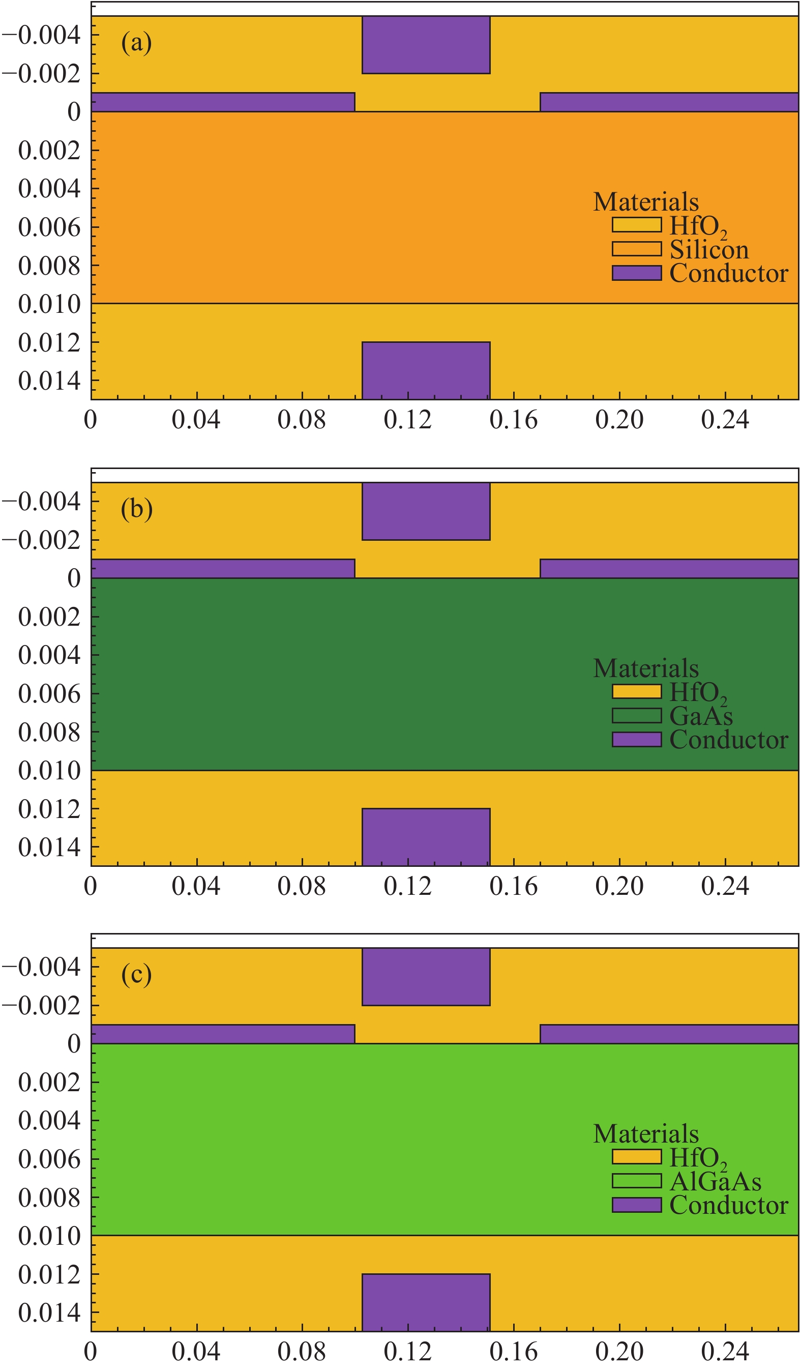
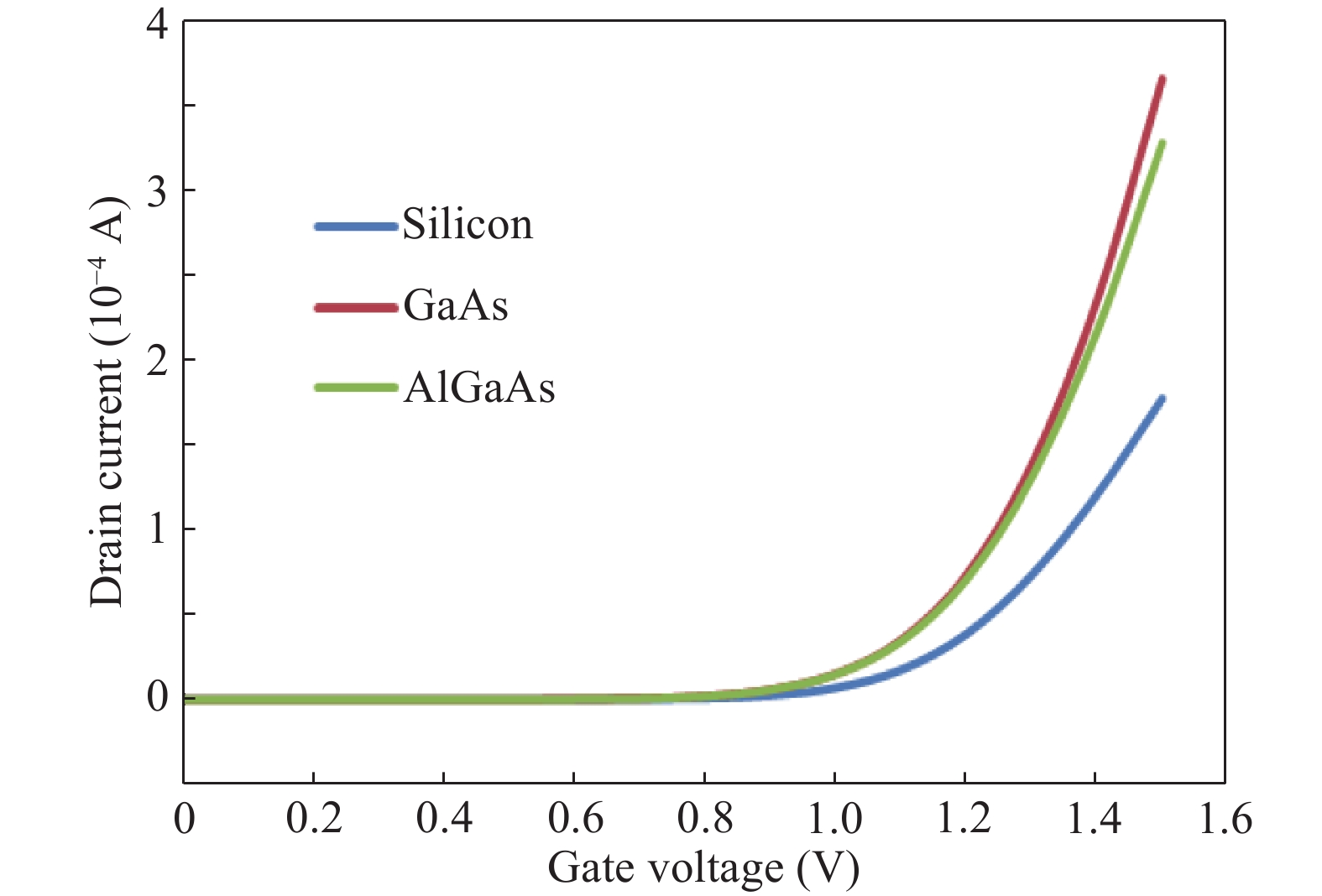
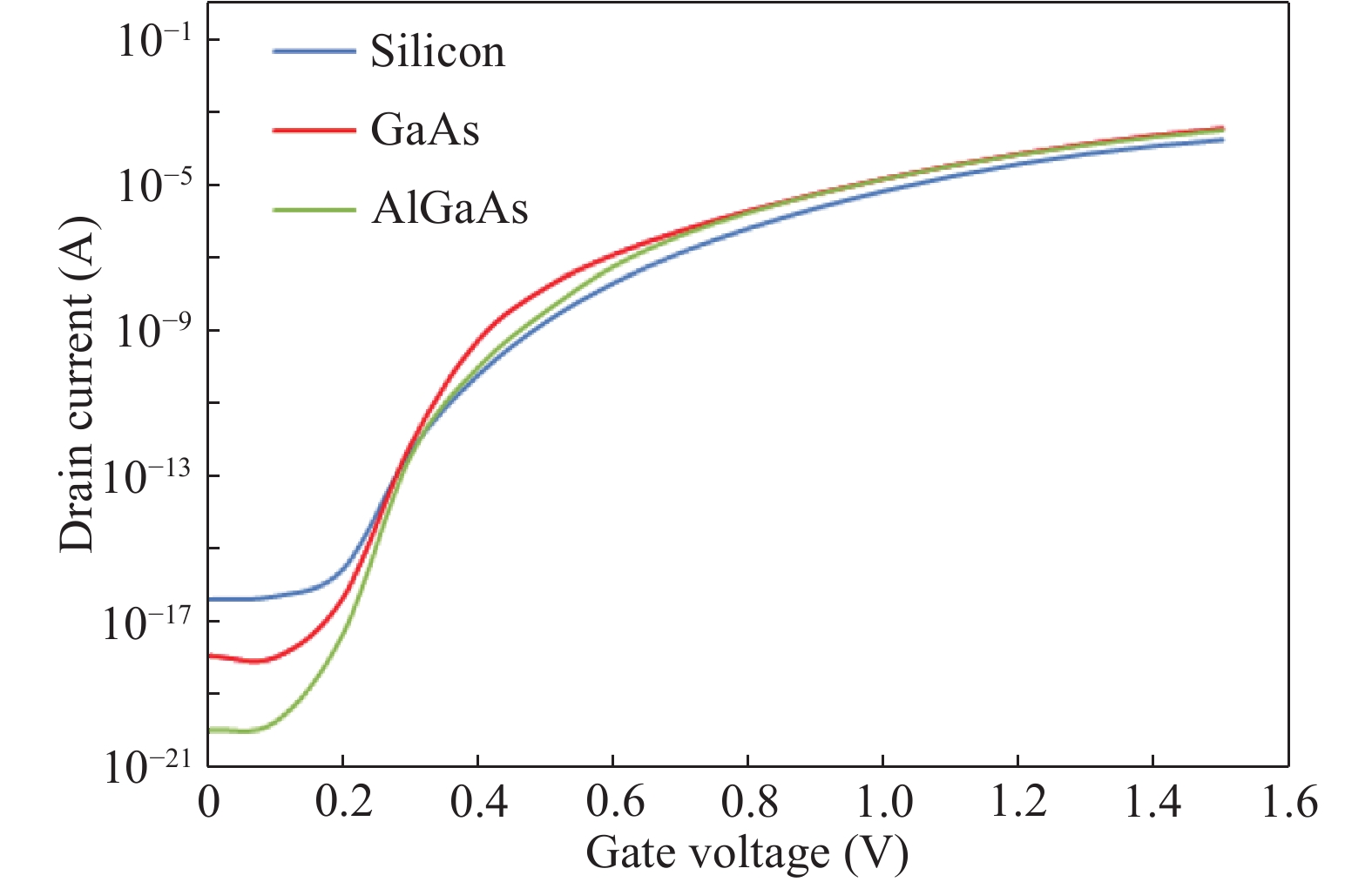
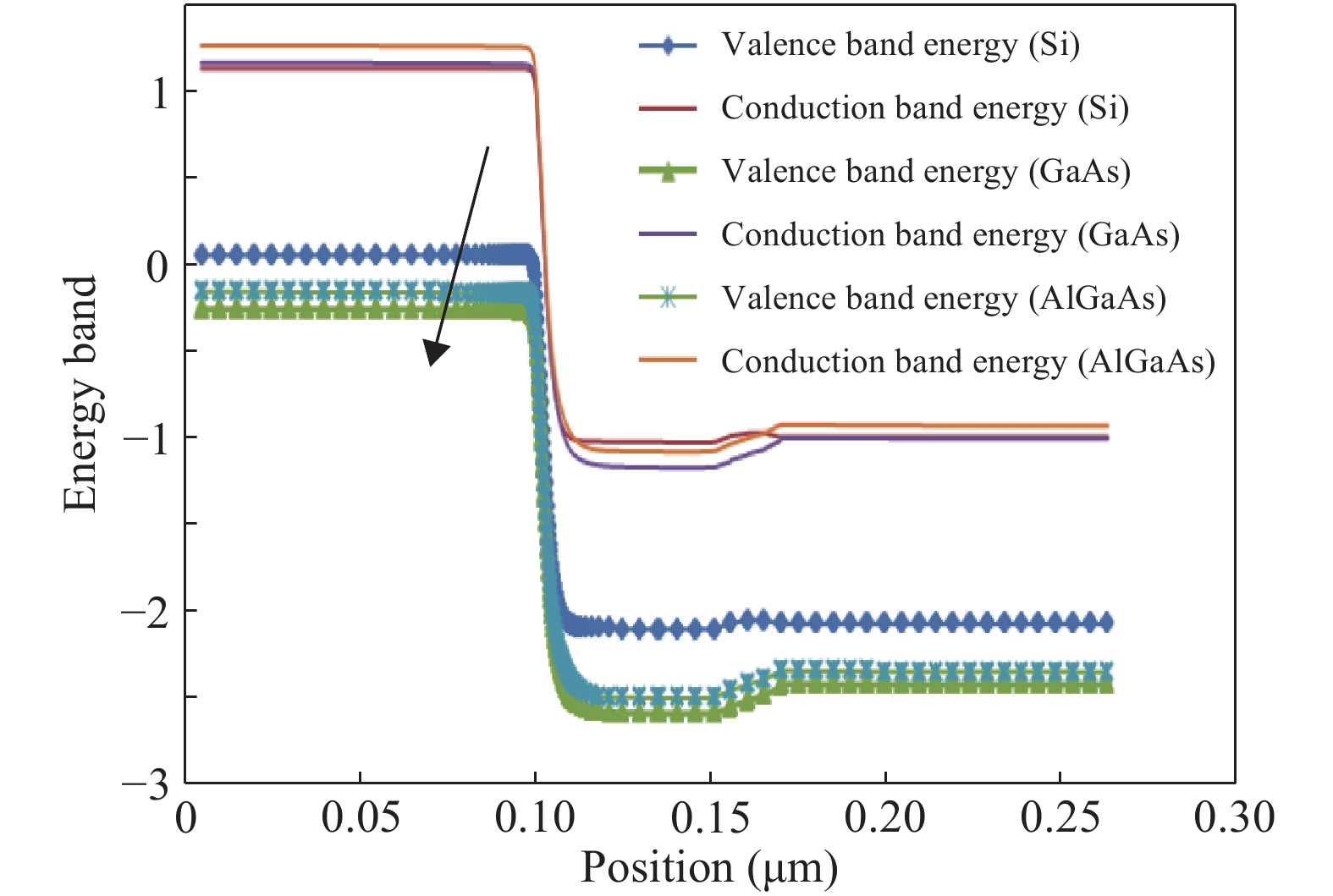
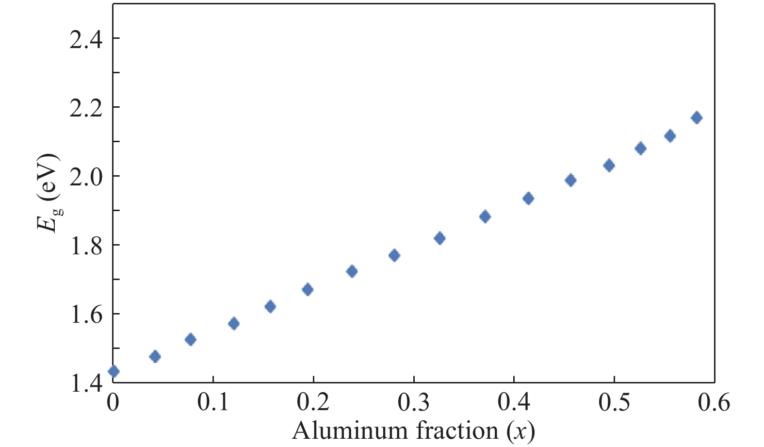
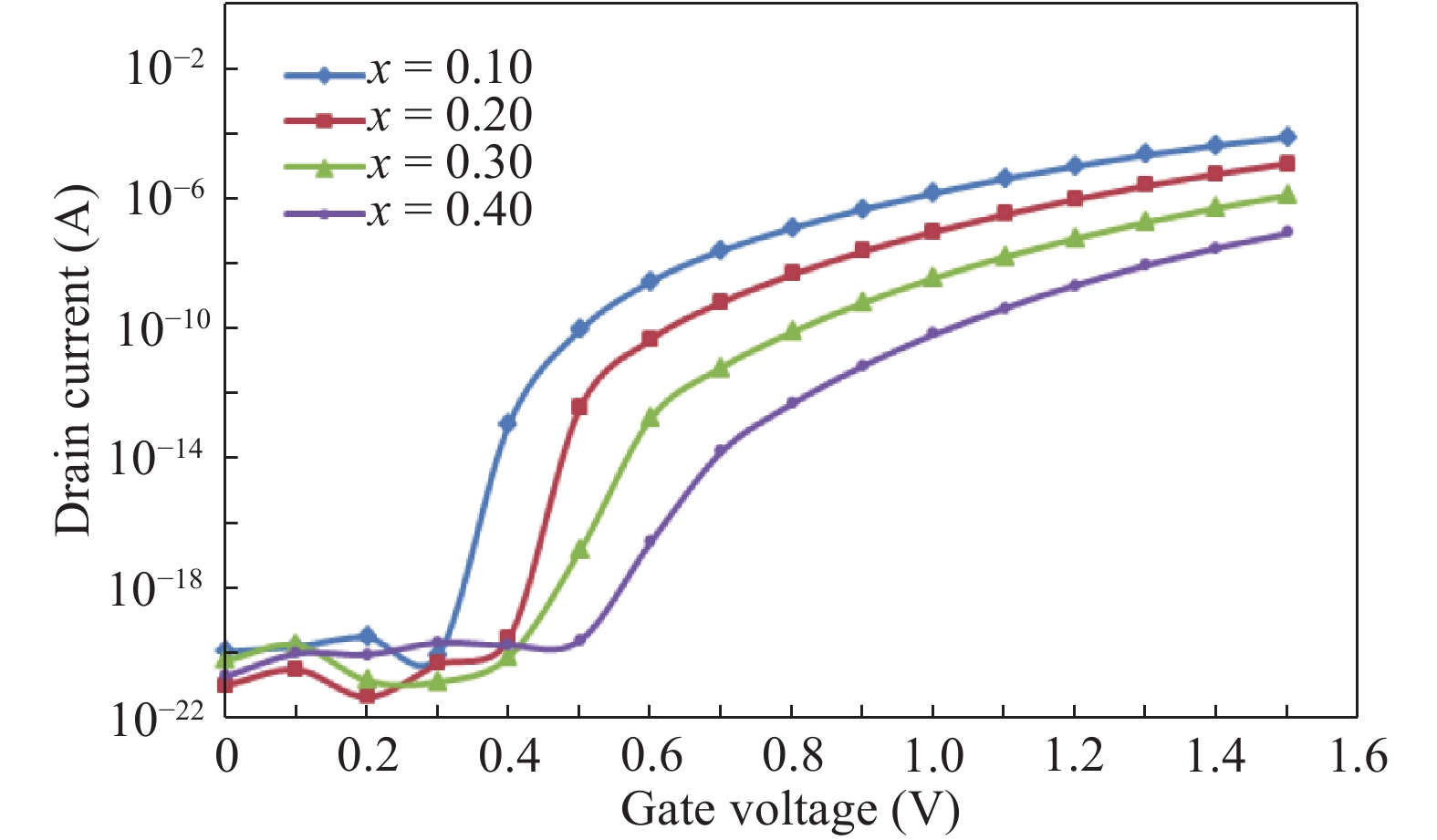
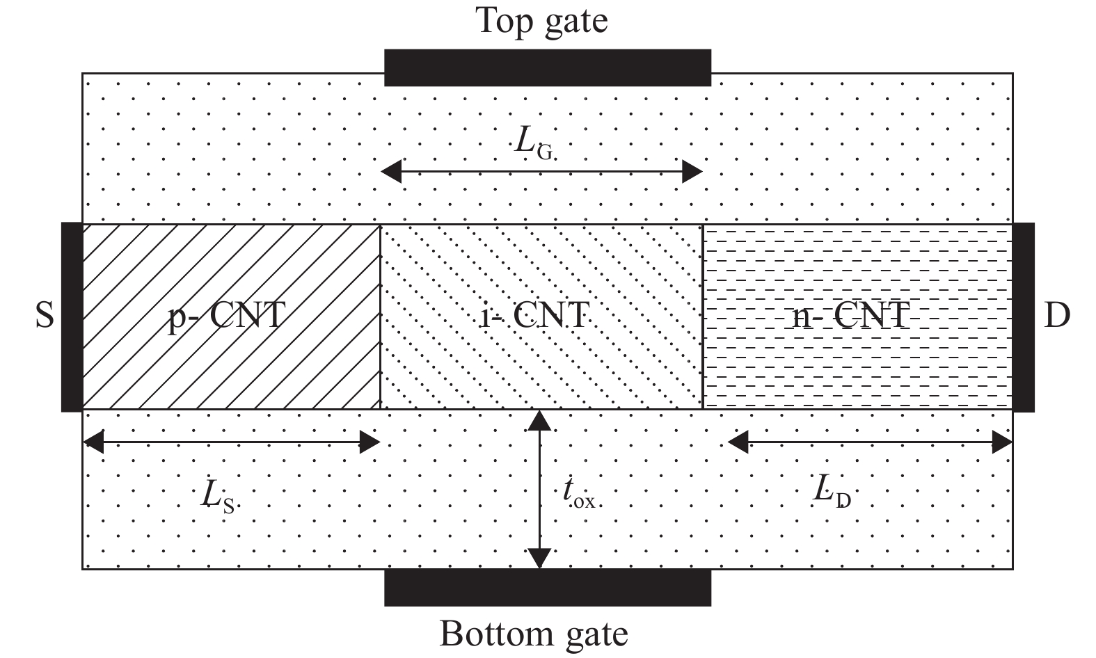
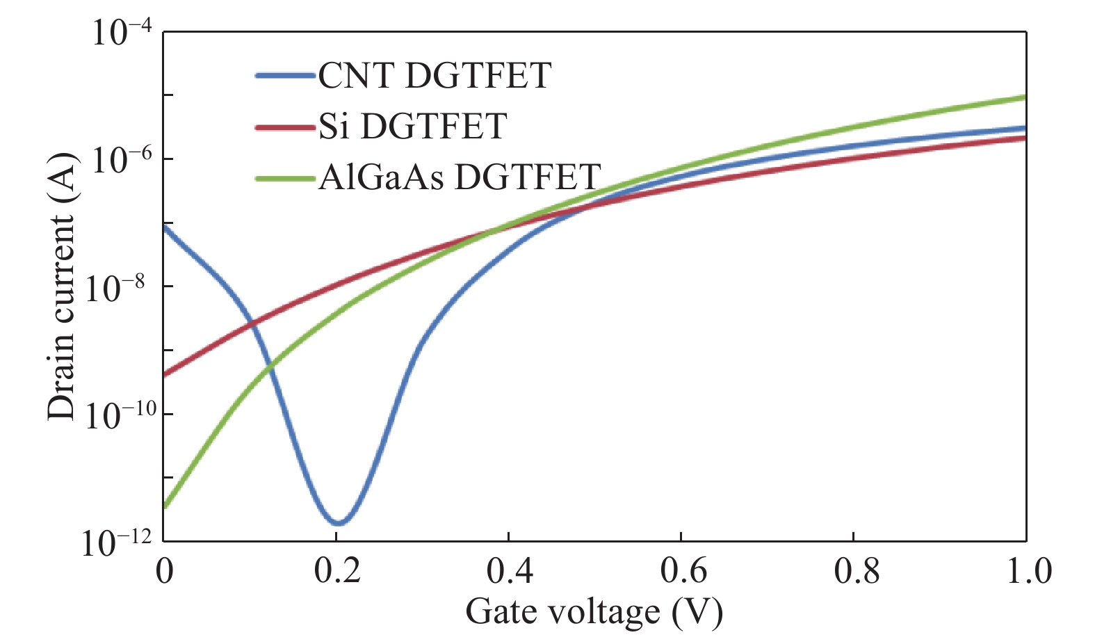
Table 1. Properties of the various channel materials used in SILVACO ATLAS TCAD simulation.
| Property | Si | GaAs | AlxGa1?xAs | CNT |
| Dielectric constant | 11.9 | 13.1 | 12.90?2.84x | 4.8 |
| Energy gap at 300 K (eV) | 1.12 | 1.424 | 1.422 eV + 1.2475x | 0.75 |
| Intrinsic carrier concentration (cm?3) | 1.45 × 10¹⁰ | 1.79 × 10⁶ | 2.1 × 10⁵ | – |
| Mobility (Drift) μn (cm2/(V·s)) | 1500 | 8500 | 8.1?2.2x + 104x2 | 79 000 |
| Mobility (Drift) μp (cm2/(V·s)) | 475 | 400 | 370?970x + 740x2 | 79 000 |
| Thermal conductivity at 300 K (W/cm·°C) | 1.5 | 0.46 | 0.55?2.12x + 2.48x2 | 6600 |
 DownLoad: CSV
Table 2. Various output parameters for different channel materials (SILVACO ATLAS TCAD simulation).
| Device with different channel materials | IOFF | ION | ION/IOFF | SS (mV/decade) | Vt |
| Silicon | 4.11 × 10?17 | 17.7 × 10?5 | 4.32 × 10¹² | 30.7985 | 0.682591 |
| GaAs | 1.16 × 10?18 | 36.6 × 10?5 | 3.15 × 10¹⁴ | 16.121 | 0.590537 |
| AlGaAs | 1.01 × 10?20 | 32.8 × 10?5 | 3.24 × 10¹⁶ | 14.5095 | 0.627576 |
DownLoad: CSV
Table 3. Various output parameters for different mole fractions of aluminum.
| Mole fraction | IOFF | ION | ION/IOFF | SS (mV/decade) | Vt |
| x = 10 | 1.24 × 10?21 | 7.70 × 10?5 | 6.21 × 10¹⁶ | 14.074 | 0.785767 |
| x = 20 | 1.18 × 10?21 | 1.19 × 10?5 | 1.01 × 10¹⁶ | 14.1381 | 1.00271 |
| x = 30 | 6.86 × 10?21 | 1.24 × 10?6 | 1.81 × 10¹⁴ | 24.6429 | 1.24419 |
| x = 40 | 2.20 × 10?21 | 8.67 × 10?8 | 3.94 × 10¹³ | 27.9075 | 1.3300 |
DownLoad: CSV
Table 4. Various output parameters for different channel materials obtained from TCAD simulation.
| Device with different channel materials | ION | IOFF | ION/IOFF | SS (mV/decade) |
| Silicon | 2.14 × 10?6 | 4.27 × 10?10 | 5.011 × 10³ | 37 |
| AlxGa1?xAs | 9.30 × 10?6 | 3.70 × 10?12 | 2.51 × 10⁶ | 32.5 |
| CNT (d = 1 nm) | 3.03 × 10?6 | 2.00 × 10?12 | 1.51 × 10⁶ | 29.4 |
DownLoad: CSV
| [1] |
Sakurai T. Perspectives of low-power VLSI's. IEICE trans Electron, 2004, 87(4): 429
|
| [2] |
Bernstein K, Cavin R K, Porod W, et al. Device and architecture outlook for beyond CMOS switches. Proc IEEE, 2010, 98(12): 2169 doi: 10.1109/JPROC.2010.2066530
|
| [3] |
Seabaugh A C, Zhang Q. Low-voltage tunnel transistors for beyond CMOS logic. Proc IEEE, 2010, 98(12): 2095 doi: 10.1109/JPROC.2010.2070470
|
| [4] |
Zener C. A theory of the electrical breakdown of solid dielectrics. Proc Royal Soc London A, 1934, 145(855): 523 doi: 10.1098/rspa.1934.0116
|
| [5] |
Silvaco ATLAS device simulator and user manual, silvaco int; Santa Clara, CA, USA 5.19.2 2013
|
| [6] |
Appenzeller J, Lin Y M, Knoch J, et al. Comparing carbon nanotube transistors-the ideal choice: a novel tunneling device design. IEEE Trans Electron Devices, 2005, 52(12): 2568 doi: 10.1109/TED.2005.859654
|
| [7] |
Sharma S K, Raj B, Khosla M. Comparative analysis of MOSFET, CNTFET and NWFET for energy efficient VLSI circuit design. J VLSI Des Tools Technol, 2016, 6: 1
|
| [8] |
Boucart K, Ionescu A M. Length scaling of the double gate tunnel FET with a high-k gate dielectric. Solid-State Electron, 2007, 51(11): 1500
|
| [9] |
Sharma S K, Raj B, Khosla M. A Gaussian approach for analytical subthreshold current model of cylindrical nanowire FET with quantum mechanical effects. Microelectron J, 2016, 53: 65 doi: 10.1016/j.mejo.2016.04.002
|
| [10] |
Sharma S K, Raj B, Khosla M. Subthreshold performance of In1?xGaxAs based dual metal with gate stack cylindrical/surrounding gate nanowire MOSFET for low power analog applications. J Nanoelectron Optoelectron, 2017, 12(2): 171 doi: 10.1166/jno.2017.1961
|
| [11] |
Zhang L, Lin X, He J, et al. An analytical charge model for double-gate tunnel FETs. IEEE Trans Electron Devices, 2012, 59(12): 3217 doi: 10.1109/TED.2012.2217145
|
| [12] |
Kumar S, Raj B. Compact channel potential analytical modeling of DG-TFET based on Evanescent-mode approach. J Comput Electron, 2015, 14(3): 820 doi: 10.1007/s10825-015-0718-9
|
| [13] |
Singh A, Khosla M, Raj B. Analysis of electrostatic doped Schottky barrier carbon nanotube FET for low power applications. J Mater Sci: Mater Electron, 2017, 28(2): 1762 doi: 10.1007/s10854-016-5723-7
|
| [14] |
Singh K, Raj B. Temperature-dependent modeling and performance evaluation of multi-walled CNT and single-walled CNT as global interconnects. J Electron Mater, 2015, 44(12): 4825 doi: 10.1007/s11664-015-4040-x
|
| [15] |
Narang R, Saxena M, Gupta M, et al. Modeling and simulation of multi layer gate dielectric double gate tunnel field-effect transistor (DG-TFET). Students' Technology Symposium (TechSym), 2011: 281
|
| [16] |
Kumar S, Raj B. Analysis of ION and ambipolar current for dual-material gate–drain overlapped DG-TFET. J Nanoelectron Optoelectron, 2016, 11(3): 323 doi: 10.1166/jno.2016.1902
|
| [17] |
Singh K, Raj B. Performance and analysis of temperature dependent multi-walled carbon nanotubes as global interconnects at different technology nodes. J Comput Electron, 2015, 14(2): 469 doi: 10.1007/s10825-015-0667-3
|
| [18] |
Krishnamohan T, Kim D, Raghunathan S, et al. Double-gate strained-Ge heterostructure tunneling FET (TFET) with record high drive currents and
|
| [19] |
Arun S, Balamurugan N B. An analytical modeling and simulation of dual material double gate tunnel field effect transistor for low power applications. J Electr Eng Technol, 2014, 9(1): 247 doi: 10.5370/JEET.2014.9.1.247
|
| [20] |
Singh A, Khosla M, Raj B. Compact model for ballistic single wall CNTFET under quantum capacitance limit. J Semicond, 2016, 37(10): 104001 doi: 10.1088/1674-4926/37/10/104001
|
| [21] |
Sahoo R, Mishra R R. Simulations of carbon nanotube field effect transistors. Int J Electron Eng Res, 2009, 1(2): 117
|
| [22] |
Singh A, Khosla M, Raj B. Compact model for ballistic single wall CNTFET under quantum capacitance limit. J Semicond, 2016, 37(10): 104001 doi: 10.1088/1674-4926/37/10/104001
|
| [23] |
Singh A, Khosla M, Raj B. Comparative analysis of carbon nanotube field effect transistor and nanowire transistor for low power circuit design. J Nanoelectron Optoelectron, 2016, 11(3): 388 doi: 10.1166/jno.2016.1913
|


Article views: 7487 Times PDF downloads: 399 Times Cited by: 0 Times
Received: 21 July 2017 Revised: 09 August 2017 Online: Uncorrected proof: 25 January 2018Accepted Manuscript: 02 March 2018Published: 01 April 2018
| Citation: |
Shashi Bala, Mamta Khosla. Design and simulation of nanoscale double-gate TFET/tunnel CNTFET[J]. Journal of Semiconductors, 2018, 39(4): 044001. doi: 10.1088/1674-4926/39/4/044001
****
S S B la, M Khosla. Design and simulation of nanoscale double-gate TFET/tunnel CNTFET[J]. J. Semicond., 2018, 39(4): 044001. doi: 10.1088/1674-4926/39/4/044001.

|
| [1] |
Sakurai T. Perspectives of low-power VLSI's. IEICE trans Electron, 2004, 87(4): 429
|
| [2] |
Bernstein K, Cavin R K, Porod W, et al. Device and architecture outlook for beyond CMOS switches. Proc IEEE, 2010, 98(12): 2169 doi: 10.1109/JPROC.2010.2066530
|
| [3] |
Seabaugh A C, Zhang Q. Low-voltage tunnel transistors for beyond CMOS logic. Proc IEEE, 2010, 98(12): 2095 doi: 10.1109/JPROC.2010.2070470
|
| [4] |
Zener C. A theory of the electrical breakdown of solid dielectrics. Proc Royal Soc London A, 1934, 145(855): 523 doi: 10.1098/rspa.1934.0116
|
| [5] |
Silvaco ATLAS device simulator and user manual, silvaco int; Santa Clara, CA, USA 5.19.2 2013
|
| [6] |
Appenzeller J, Lin Y M, Knoch J, et al. Comparing carbon nanotube transistors-the ideal choice: a novel tunneling device design. IEEE Trans Electron Devices, 2005, 52(12): 2568 doi: 10.1109/TED.2005.859654
|
| [7] |
Sharma S K, Raj B, Khosla M. Comparative analysis of MOSFET, CNTFET and NWFET for energy efficient VLSI circuit design. J VLSI Des Tools Technol, 2016, 6: 1
|
| [8] |
Boucart K, Ionescu A M. Length scaling of the double gate tunnel FET with a high-k gate dielectric. Solid-State Electron, 2007, 51(11): 1500
|
| [9] |
Sharma S K, Raj B, Khosla M. A Gaussian approach for analytical subthreshold current model of cylindrical nanowire FET with quantum mechanical effects. Microelectron J, 2016, 53: 65 doi: 10.1016/j.mejo.2016.04.002
|
| [10] |
Sharma S K, Raj B, Khosla M. Subthreshold performance of In1?xGaxAs based dual metal with gate stack cylindrical/surrounding gate nanowire MOSFET for low power analog applications. J Nanoelectron Optoelectron, 2017, 12(2): 171 doi: 10.1166/jno.2017.1961
|
| [11] |
Zhang L, Lin X, He J, et al. An analytical charge model for double-gate tunnel FETs. IEEE Trans Electron Devices, 2012, 59(12): 3217 doi: 10.1109/TED.2012.2217145
|
| [12] |
Kumar S, Raj B. Compact channel potential analytical modeling of DG-TFET based on Evanescent-mode approach. J Comput Electron, 2015, 14(3): 820 doi: 10.1007/s10825-015-0718-9
|
| [13] |
Singh A, Khosla M, Raj B. Analysis of electrostatic doped Schottky barrier carbon nanotube FET for low power applications. J Mater Sci: Mater Electron, 2017, 28(2): 1762 doi: 10.1007/s10854-016-5723-7
|
| [14] |
Singh K, Raj B. Temperature-dependent modeling and performance evaluation of multi-walled CNT and single-walled CNT as global interconnects. J Electron Mater, 2015, 44(12): 4825 doi: 10.1007/s11664-015-4040-x
|
| [15] |
Narang R, Saxena M, Gupta M, et al. Modeling and simulation of multi layer gate dielectric double gate tunnel field-effect transistor (DG-TFET). Students' Technology Symposium (TechSym), 2011: 281
|
| [16] |
Kumar S, Raj B. Analysis of ION and ambipolar current for dual-material gate–drain overlapped DG-TFET. J Nanoelectron Optoelectron, 2016, 11(3): 323 doi: 10.1166/jno.2016.1902
|
| [17] |
Singh K, Raj B. Performance and analysis of temperature dependent multi-walled carbon nanotubes as global interconnects at different technology nodes. J Comput Electron, 2015, 14(2): 469 doi: 10.1007/s10825-015-0667-3
|
| [18] |
Krishnamohan T, Kim D, Raghunathan S, et al. Double-gate strained-Ge heterostructure tunneling FET (TFET) with record high drive currents and
|
| [19] |
Arun S, Balamurugan N B. An analytical modeling and simulation of dual material double gate tunnel field effect transistor for low power applications. J Electr Eng Technol, 2014, 9(1): 247 doi: 10.5370/JEET.2014.9.1.247
|
| [20] |
Singh A, Khosla M, Raj B. Compact model for ballistic single wall CNTFET under quantum capacitance limit. J Semicond, 2016, 37(10): 104001 doi: 10.1088/1674-4926/37/10/104001
|
| [21] |
Sahoo R, Mishra R R. Simulations of carbon nanotube field effect transistors. Int J Electron Eng Res, 2009, 1(2): 117
|
| [22] |
Singh A, Khosla M, Raj B. Compact model for ballistic single wall CNTFET under quantum capacitance limit. J Semicond, 2016, 37(10): 104001 doi: 10.1088/1674-4926/37/10/104001
|
| [23] |
Singh A, Khosla M, Raj B. Comparative analysis of carbon nanotube field effect transistor and nanowire transistor for low power circuit design. J Nanoelectron Optoelectron, 2016, 11(3): 388 doi: 10.1166/jno.2016.1913
|

 WeChat ID
Journal of Semiconductors © 2017 All Rights Reserved 京ICP備05085259號-2