


Fig. 2.
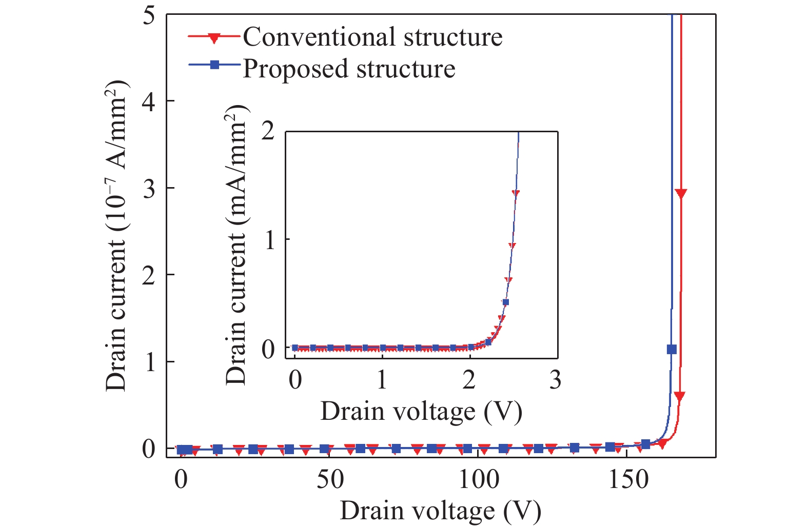
?(Color?online)?Simulated results of the breakdown voltage and threshold voltage for two structures.
SEMICONDUCTOR DEVICES
Jiang Lu1, , Hainan Liu1, Xiaowu Cai1, Jiajun Luo1, 2, 3, Bo Li1, 2, Binhong Li1, 2, Lixin Wang1, 2, 3 and Zhengsheng Han1, 2, 3
Corresponding author: Jiang Lu, Email: lujiang@ime.ac.cn
Abstract: We present a single-event burnout (SEB) hardened planar power MOSFET with partially widened trench sources by three-dimensional (3D) numerical simulation. The advantage of the proposed structure is that the work of the parasitic bipolar transistor inherited in the power MOSFET is suppressed effectively due to the elimination of the most sensitive region (P-well region below the N+ source). The simulation result shows that the proposed structure can enhance the SEB survivability significantly. The critical value of linear energy transfer (LET), which indicates the maximum deposited energy on the device without SEB behavior, increases from 0.06 to 0.7 pC/μm. The SEB threshold voltage increases to 120 V, which is 80% of the rated breakdown voltage. Meanwhile, the main parameter characteristics of the proposed structure remain similar with those of the conventional planar structure. Therefore, this structure offers a potential optimization path to planar power MOSFET with high SEB survivability for space and atmospheric applications.
Key words: planar power MOSFETs, single-event burnout (SEB), parasitic bipolar transistor, second breakdown voltage
| [1] |
Titus J L. An updated perspective of single event gate rupture and single event burnout in power MOSFETs. IEEE Trans Nucl Sci, 2013, 60(3): 1912 doi: 10.1109/TNS.2013.2252194
|
| [2] |
Liu S, Titus J L, Boden M. Effect of buffer layer on single-event burnout of power DMOSFETs. IEEE Trans Nucl Sci, 2007, 54(6): 2554 doi: 10.1109/TNS.2007.910869
|
| [3] |
Wang Y, Zhang Y, Wang L G, et al. Single-event burnout hardening of power UMOSFETs with optimized structure. IEEE Trans Electron Devices, 2013, 60(3): 2001
|
| [4] |
Wang Y, Yu C H, Dou Z, et al. Single-event burnout hardening of power UMOSFETs with integrated schottky diode. IEEE Trans Electron Devices, 2014, 61(5): 1464 doi: 10.1109/TED.2014.2312948
|
| [5] |
Ying W, Yu C H, Cao F, et al. Simulation study of single event effects for split-gate enhanced power U-shape metal–oxide semiconductor field-effect transistor. IET Power Electron Lett, 2014, 7(12): 2895 doi: 10.1049/iet-pel.2013.0633
|
| [6] |
Yu C H, Wang Y, Cao F, et al. Research of single-event burnout in power planar VDMOSFETs by localized carrier lifetime control. IEEE Trans Electron Devices, 2015, 62(1): 143 doi: 10.1109/TED.2014.2365817
|
| [7] |
Wan X, Zhou W S, Ren S, et al. SEB hardened power MOSFETs with high-k dielectrics. IEEE Trans Nucl Sci, 2015, 62(6): 2830 doi: 10.1109/TNS.2015.2498145
|
| [8] |
Jia Y P, Su H Y, Jin R, et al. Simulation study on single event burnout in linear doping buffer layer engineered power VDMOSFET. J Semicond, 2016, 37(2): 024008 doi: 10.1088/1674-4926/37/2/024008
|
| [9] |
Wang Y, Yu C H, Li M S, et al. High-performance split-gate-enhanced UMOSFET with dual channels. IEEE Trans Electron Devices, 2017, 64(4): 1455 doi: 10.1109/TED.2017.2665589
|
| [10] |
Sumitomo M, Asai J, Sakane H, et al. Low loss IGBT with partially narrow mesa structure (PNM-IGBT). Proceeding of 24th International Symposium on Power Semiconductor Devices & IC’S. Bruges, Belgium, 2012
|
| [11] |
Lu J, Wang L X, Lu S J, et al. Avalanche behavior of power MOSFETs under different temperature conditions. J Semicond, 2011, 32(1): 014001 doi: 10.1088/1674-4926/32/1/014001
|
| [12] |
Luu A, Austin P, Miller F, et al. Sensitive volume and triggering criteria of SEB in classic planar VDMOS. IEEE Trans Nucl Sci, 2010, 57(4): 1900 doi: 10.1109/TNS.2010.2044808
|
| [13] |
Ji I H, Cho K H, Han M K, et al. New power MOSFET employing segmented trench body contact for improving the avalanche energy. Proceeding of 20th International Symposium on Power Semiconductor Devices & IC’s, Orlando, USA, 2008
|
| [14] |
Siconolfi S, Hubert G, Artola L, et al. A physical prediction model issued from TCAD investigations for single event burnout in power MOSFETs. 14th European Conference on Radiation and Its Effects on Components and Systems, Oxford, UK, 2013
|
| [15] |
Baliga B J. Fundamentals of power semiconductor devices. New York, Springer Science & Business Media, 2008: 449
|
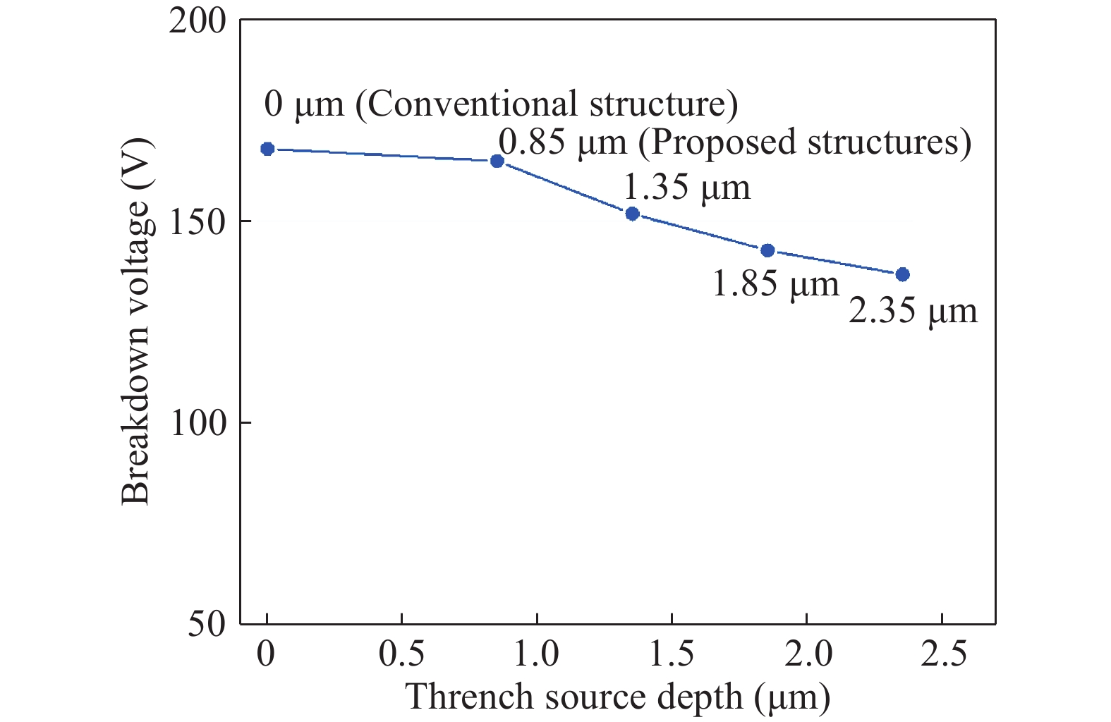
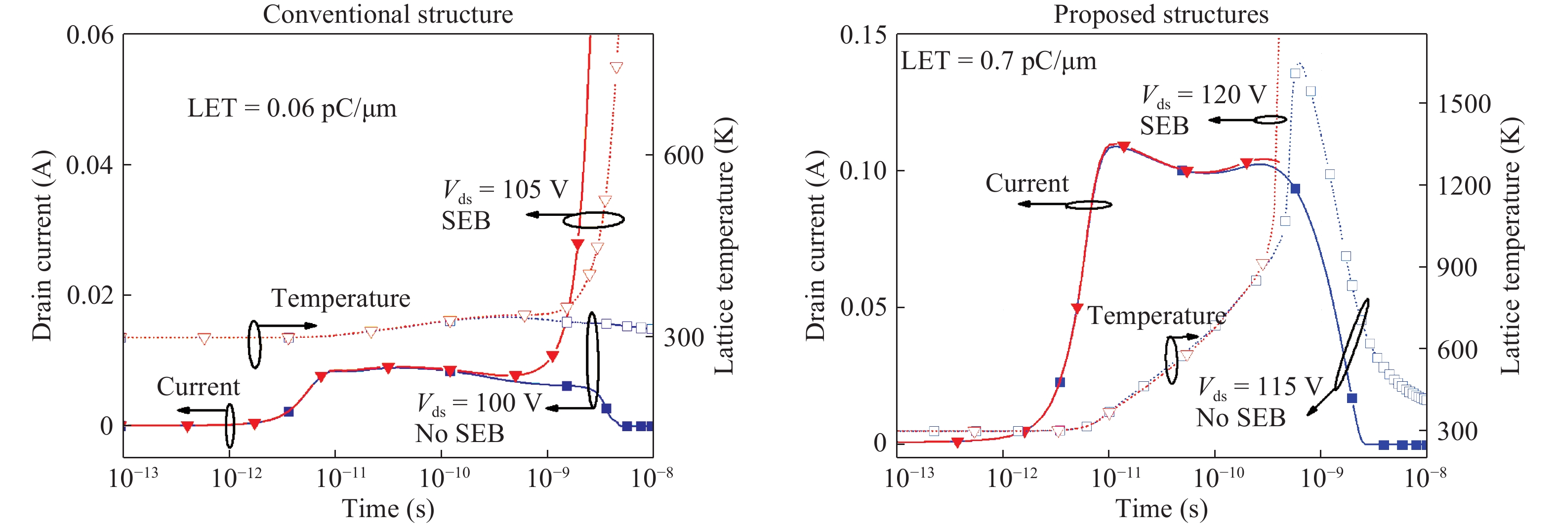
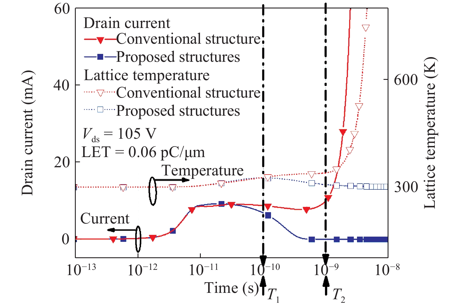
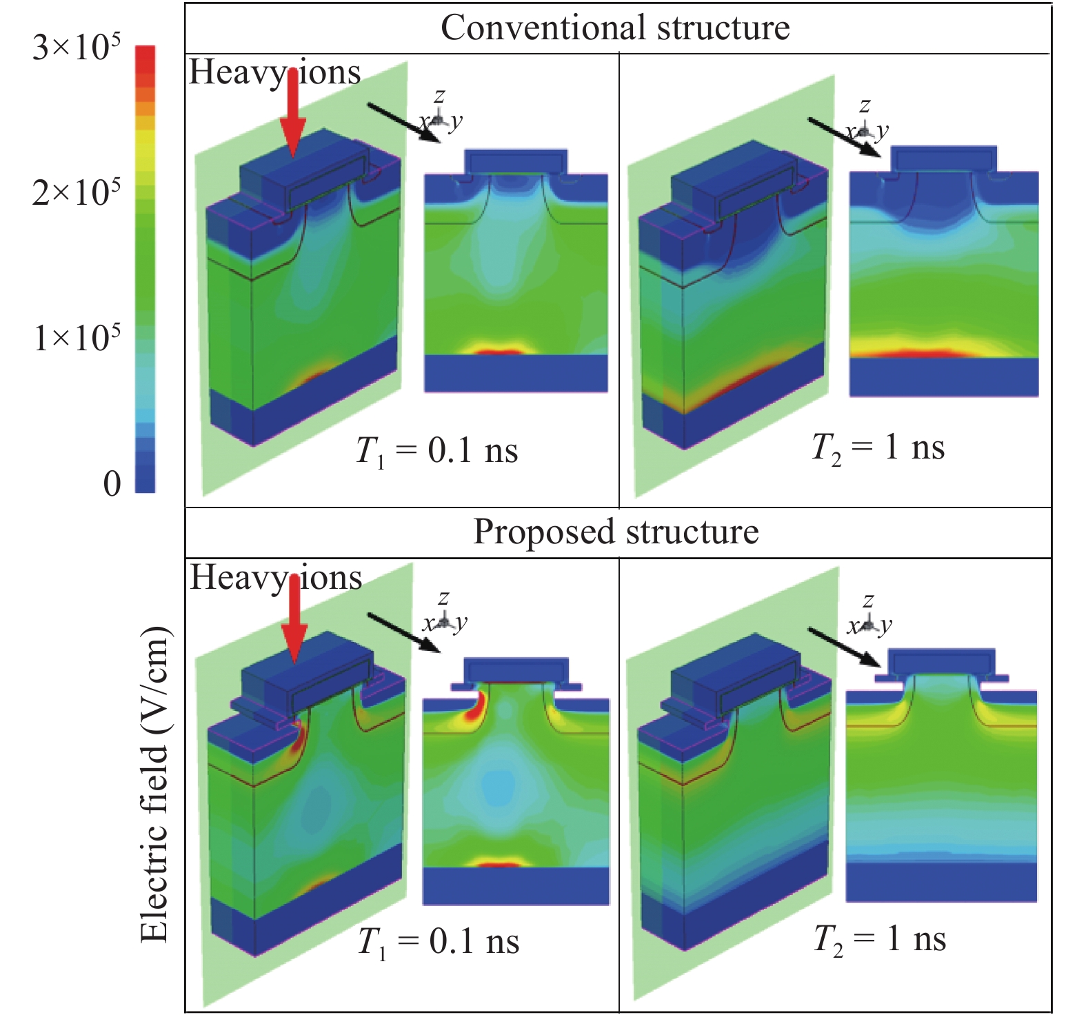
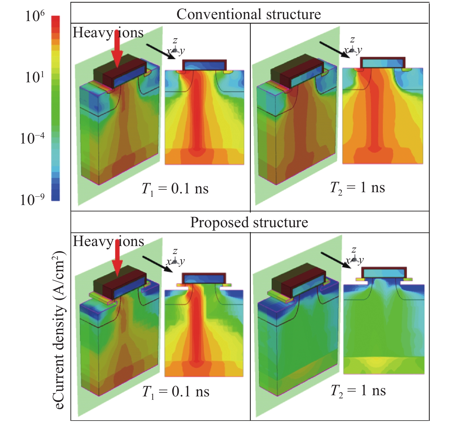
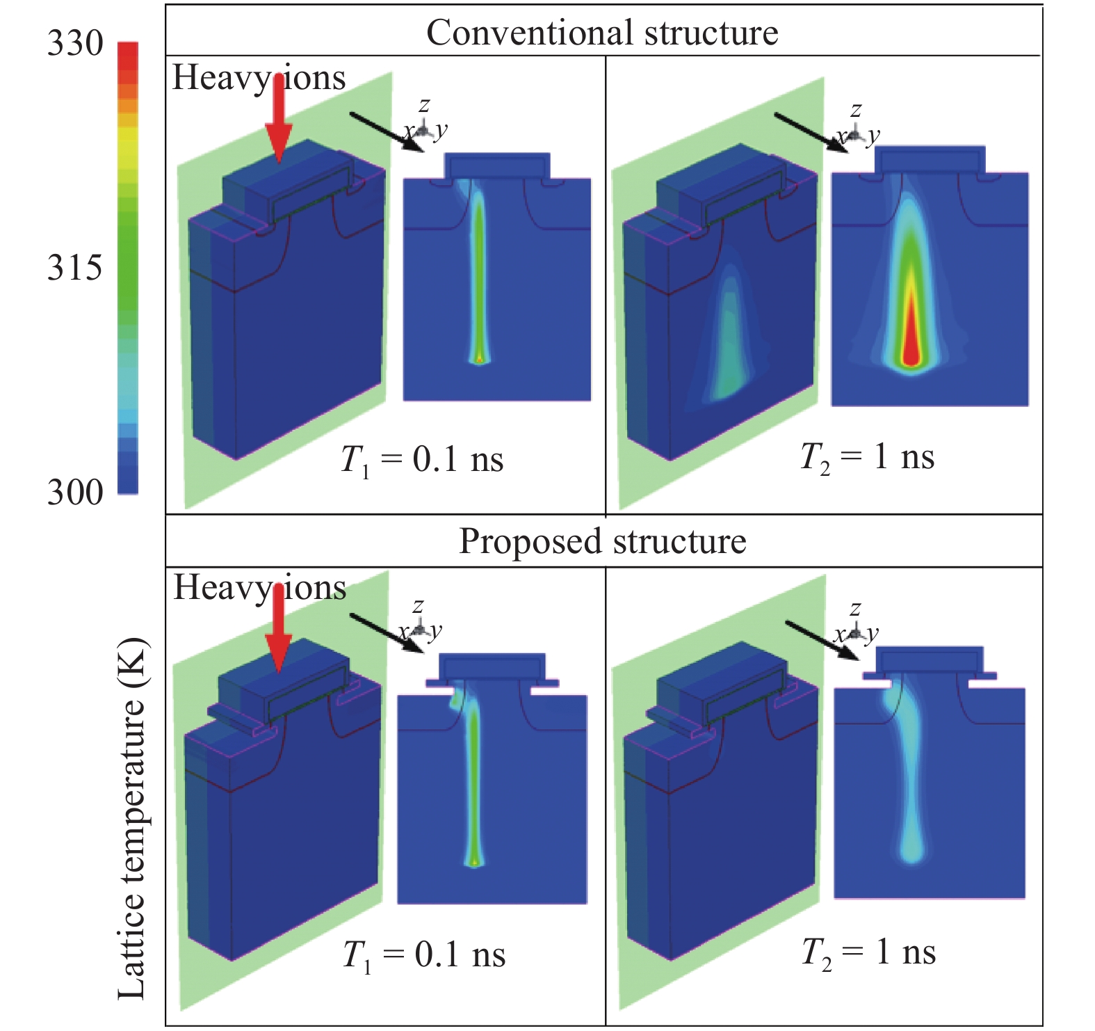
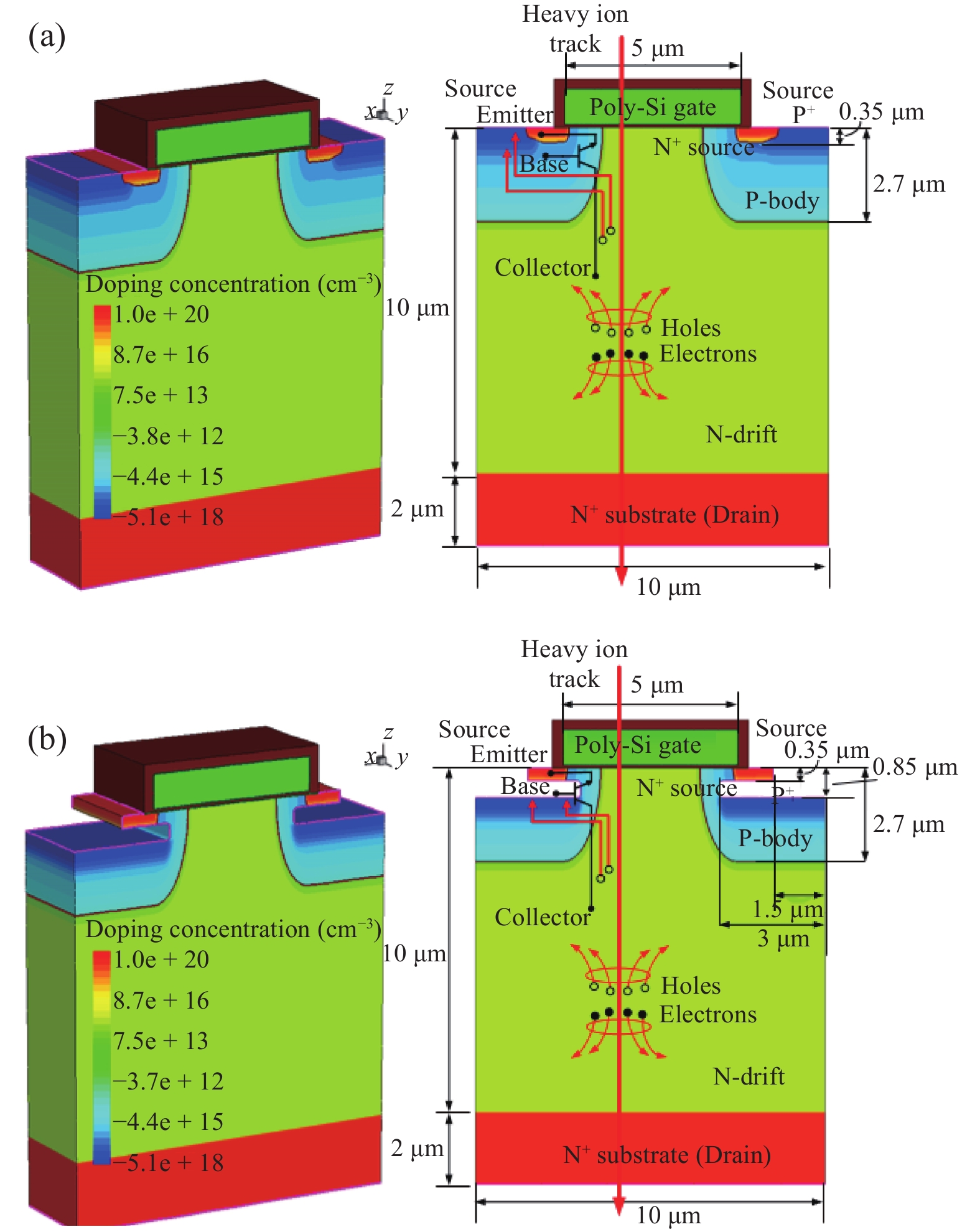
Table 1. Major structural parameters for the simulation.
| Structure parameter | Conventional
planar structure |
Proposed structure |
| Cell pitch (μm) | 10 | 10 |
| N-drift thickness (μm) | 10 | 10 |
| Gate oxide thickness (nm) | 100 | 100 |
| Gate poly width (μm) | 5 | 5 |
| N-drift doping (1015 cm?3) | 2 | 2 |
| P-body depth (μm) | 2.7 | 2.7 |
| P-body doping (1016 cm?3) | 8 | 8 |
| N+ depth (μm) | 0.35 | 0.35 |
| N+ width (μm) | 0.5 | 0.5 |
| N+ doping (1020 cm?3) | 1 | 1 |
| P+ doping (1018 cm?3) | 5 | 5 |
| Trench source depth (μm) | ? | 0.85 |
| Trench source width (μm) | ? | 6 |
| Partially widened trench source width (μm) | ? | 6 |
 DownLoad: CSV
| [1] |
Titus J L. An updated perspective of single event gate rupture and single event burnout in power MOSFETs. IEEE Trans Nucl Sci, 2013, 60(3): 1912 doi: 10.1109/TNS.2013.2252194
|
| [2] |
Liu S, Titus J L, Boden M. Effect of buffer layer on single-event burnout of power DMOSFETs. IEEE Trans Nucl Sci, 2007, 54(6): 2554 doi: 10.1109/TNS.2007.910869
|
| [3] |
Wang Y, Zhang Y, Wang L G, et al. Single-event burnout hardening of power UMOSFETs with optimized structure. IEEE Trans Electron Devices, 2013, 60(3): 2001
|
| [4] |
Wang Y, Yu C H, Dou Z, et al. Single-event burnout hardening of power UMOSFETs with integrated schottky diode. IEEE Trans Electron Devices, 2014, 61(5): 1464 doi: 10.1109/TED.2014.2312948
|
| [5] |
Ying W, Yu C H, Cao F, et al. Simulation study of single event effects for split-gate enhanced power U-shape metal–oxide semiconductor field-effect transistor. IET Power Electron Lett, 2014, 7(12): 2895 doi: 10.1049/iet-pel.2013.0633
|
| [6] |
Yu C H, Wang Y, Cao F, et al. Research of single-event burnout in power planar VDMOSFETs by localized carrier lifetime control. IEEE Trans Electron Devices, 2015, 62(1): 143 doi: 10.1109/TED.2014.2365817
|
| [7] |
Wan X, Zhou W S, Ren S, et al. SEB hardened power MOSFETs with high-k dielectrics. IEEE Trans Nucl Sci, 2015, 62(6): 2830 doi: 10.1109/TNS.2015.2498145
|
| [8] |
Jia Y P, Su H Y, Jin R, et al. Simulation study on single event burnout in linear doping buffer layer engineered power VDMOSFET. J Semicond, 2016, 37(2): 024008 doi: 10.1088/1674-4926/37/2/024008
|
| [9] |
Wang Y, Yu C H, Li M S, et al. High-performance split-gate-enhanced UMOSFET with dual channels. IEEE Trans Electron Devices, 2017, 64(4): 1455 doi: 10.1109/TED.2017.2665589
|
| [10] |
Sumitomo M, Asai J, Sakane H, et al. Low loss IGBT with partially narrow mesa structure (PNM-IGBT). Proceeding of 24th International Symposium on Power Semiconductor Devices & IC’S. Bruges, Belgium, 2012
|
| [11] |
Lu J, Wang L X, Lu S J, et al. Avalanche behavior of power MOSFETs under different temperature conditions. J Semicond, 2011, 32(1): 014001 doi: 10.1088/1674-4926/32/1/014001
|
| [12] |
Luu A, Austin P, Miller F, et al. Sensitive volume and triggering criteria of SEB in classic planar VDMOS. IEEE Trans Nucl Sci, 2010, 57(4): 1900 doi: 10.1109/TNS.2010.2044808
|
| [13] |
Ji I H, Cho K H, Han M K, et al. New power MOSFET employing segmented trench body contact for improving the avalanche energy. Proceeding of 20th International Symposium on Power Semiconductor Devices & IC’s, Orlando, USA, 2008
|
| [14] |
Siconolfi S, Hubert G, Artola L, et al. A physical prediction model issued from TCAD investigations for single event burnout in power MOSFETs. 14th European Conference on Radiation and Its Effects on Components and Systems, Oxford, UK, 2013
|
| [15] |
Baliga B J. Fundamentals of power semiconductor devices. New York, Springer Science & Business Media, 2008: 449
|


Article views: 5088 Times PDF downloads: 125 Times Cited by: 0 Times
Received: 23 June 2017 Revised: 21 August 2017 Online: Uncorrected proof: 24 January 2018Published: 01 March 2018
| Citation: |
Jiang Lu, Hainan Liu, Xiaowu Cai, Jiajun Luo, Bo Li, Binhong Li, Lixin Wang, Zhengsheng Han. Single-event burnout hardening of planar power MOSFET with partially widened trench source[J]. Journal of Semiconductors, 2018, 39(3): 034003. doi: 10.1088/1674-4926/39/3/034003
****
J Lu, H N Liu, X W Cai, J J Luo, B Li, B H Li, L X Wang, Z S Han. Single-event burnout hardening of planar power MOSFET with partially widened trench source[J]. J. Semicond., 2018, 39(3): 034003. doi: 10.1088/1674-4926/39/3/034003.

|
Project supported by the National Natural Science Foundation of China (Nos. 61404161, 61404068, 61404169).
| [1] |
Titus J L. An updated perspective of single event gate rupture and single event burnout in power MOSFETs. IEEE Trans Nucl Sci, 2013, 60(3): 1912 doi: 10.1109/TNS.2013.2252194
|
| [2] |
Liu S, Titus J L, Boden M. Effect of buffer layer on single-event burnout of power DMOSFETs. IEEE Trans Nucl Sci, 2007, 54(6): 2554 doi: 10.1109/TNS.2007.910869
|
| [3] |
Wang Y, Zhang Y, Wang L G, et al. Single-event burnout hardening of power UMOSFETs with optimized structure. IEEE Trans Electron Devices, 2013, 60(3): 2001
|
| [4] |
Wang Y, Yu C H, Dou Z, et al. Single-event burnout hardening of power UMOSFETs with integrated schottky diode. IEEE Trans Electron Devices, 2014, 61(5): 1464 doi: 10.1109/TED.2014.2312948
|
| [5] |
Ying W, Yu C H, Cao F, et al. Simulation study of single event effects for split-gate enhanced power U-shape metal–oxide semiconductor field-effect transistor. IET Power Electron Lett, 2014, 7(12): 2895 doi: 10.1049/iet-pel.2013.0633
|
| [6] |
Yu C H, Wang Y, Cao F, et al. Research of single-event burnout in power planar VDMOSFETs by localized carrier lifetime control. IEEE Trans Electron Devices, 2015, 62(1): 143 doi: 10.1109/TED.2014.2365817
|
| [7] |
Wan X, Zhou W S, Ren S, et al. SEB hardened power MOSFETs with high-k dielectrics. IEEE Trans Nucl Sci, 2015, 62(6): 2830 doi: 10.1109/TNS.2015.2498145
|
| [8] |
Jia Y P, Su H Y, Jin R, et al. Simulation study on single event burnout in linear doping buffer layer engineered power VDMOSFET. J Semicond, 2016, 37(2): 024008 doi: 10.1088/1674-4926/37/2/024008
|
| [9] |
Wang Y, Yu C H, Li M S, et al. High-performance split-gate-enhanced UMOSFET with dual channels. IEEE Trans Electron Devices, 2017, 64(4): 1455 doi: 10.1109/TED.2017.2665589
|
| [10] |
Sumitomo M, Asai J, Sakane H, et al. Low loss IGBT with partially narrow mesa structure (PNM-IGBT). Proceeding of 24th International Symposium on Power Semiconductor Devices & IC’S. Bruges, Belgium, 2012
|
| [11] |
Lu J, Wang L X, Lu S J, et al. Avalanche behavior of power MOSFETs under different temperature conditions. J Semicond, 2011, 32(1): 014001 doi: 10.1088/1674-4926/32/1/014001
|
| [12] |
Luu A, Austin P, Miller F, et al. Sensitive volume and triggering criteria of SEB in classic planar VDMOS. IEEE Trans Nucl Sci, 2010, 57(4): 1900 doi: 10.1109/TNS.2010.2044808
|
| [13] |
Ji I H, Cho K H, Han M K, et al. New power MOSFET employing segmented trench body contact for improving the avalanche energy. Proceeding of 20th International Symposium on Power Semiconductor Devices & IC’s, Orlando, USA, 2008
|
| [14] |
Siconolfi S, Hubert G, Artola L, et al. A physical prediction model issued from TCAD investigations for single event burnout in power MOSFETs. 14th European Conference on Radiation and Its Effects on Components and Systems, Oxford, UK, 2013
|
| [15] |
Baliga B J. Fundamentals of power semiconductor devices. New York, Springer Science & Business Media, 2008: 449
|

 WeChat ID
Journal of Semiconductors © 2017 All Rights Reserved 京ICP備05085259號(hào)-2

