


Fig. 1.
The solving steps of anisotropic thermal-stress of TSV.
SEMICONDUCTOR TECHNOLOGY
Corresponding author: Guangbao Shan, email: 18092060235@189.cn
Abstract: A two-dimensional thermal-stress model of through-silicon via (TSV) is proposed considering the anisotropic elastic property of the silicon substrate. By using the complex variable approach, the distribution of thermal-stress in the substrate can be characterized more accurately. TCAD 3-D simulations are used to verify the model accuracy and well agree with analytical results (< ±5%). The proposed thermal-stress model can be integrated into stress-driven design flow for 3-D IC , leading to the more accurate timing analysis considering the thermal-stress effect.
Key words: 3-D IC, through-silicon via, thermal-stress, TCAD simulation
| [1] |
Waldrop M M. More than Moore. Nature, 2016, 530(7589): 144 doi: 10.1038/530144a
|
| [2] |
Shen W W, Chen K N. Three-dimensional integrated circuit (3D IC) key technology: through-silicon via (TSV). Nanoscale Res Lett, 2017, 12(1): 56 doi: 10.1186/s11671-017-1831-4
|
| [3] |
Tsai H Y, Kuo C W. Thermal stress and failure location analysis for through silicon via in 3D integration. J Mechan, 2016, 32(01): 47
|
| [4] |
Johnson R W, Shen Y L. Analysis of thermal stress and its influence on carrier mobility in three-dimensional microelectronic chip stack. J Electron Pack, 2015, 137(2): 021011 doi: 10.1115/1.4029345
|
| [5] |
Ryu S K, Zhao Q, Hecker M, et al. Micro-Raman spectroscopy and analysis of near-surface stresses in silicon around through-silicon vias for three-dimensional interconnects. J Appl Phys, 2012, 111(6): 063513 doi: 10.1063/1.3696980
|
| [6] |
Athikulwongse K, Yang J S, Pan D Z, et al. Impact of mechanical stress on the full chip timing for through-silicon-via-based 3-D ICs. IEEE Trans Comput-Aid Des Integr Circuits Syst, 2013, 32(6): 905 doi: 10.1109/TCAD.2013.2237770
|
| [7] |
Chen C. Characterization of in-plane stress in TSV array—a unit model approach. Proceed IEEE, 2014: 2020
|
| [8] |
Marella S K, Sapatnekar S S. A holistic analysis of circuit performance variations in 3-D ICs with thermal and TSV-induced stress considerations. IEEE Trans Very Large Scale Integr (VLSI) Syst, 2015, 23(7): 1308 doi: 10.1109/TVLSI.2014.2335154
|
| [9] |
Li Y, Pan D Z. An accurate semi-analytical framework for full-chip TSV-induced stress modeling. Proceedings of the 50th ACM ADAC, 2013: 181
|
| [10] |
McDonough C, Backes B, Wang W, et al. Thermal and spatial profiling of TSV-induced stress in 3DICs. Proc IEEE, 2011: 5D.2.1
|
| [11] |
Jung M, Mitra J, Pan D Z, et al. TSV stress-aware full-chip mechanical reliability analysis and optimization for 3D IC. Commun ACM, 2014, 57(1): 107 doi: 10.1145/2541883
|
| [12] |
Roh M H, Sharma A, Lee J H, et al. Extrusion suppression of TSV filling metal by Cu-W electroplating for three-dimensional microelectronic packaging. Metallurg Mater Transa A, 2015, 46(5): 2051 doi: 10.1007/s11661-015-2801-z
|
| [13] |
Timoshenko S P, Goodier J N. Theory of elasticity. New York: McGraw-Hill, 1951
|
| [14] |
Lekhnitskii S G. Anisotropic plates. New York: Science Publishers, Inc., 1968
|
| [15] |
Chiang C R. Thermal mismatch stress of a cylindrical inclusion in a cubic crystal. Eng Fract Mechan, 2008, 75(8): 2295 doi: 10.1016/j.engfracmech.2007.09.002
|
| [16] |
Lekhnitskij, S. G. Theory of the elasticity of anisotropic bodies. 1977
|
| [17] |
Interconnect T S. Manual and user guide. Synopsys, Inc, 2014
|
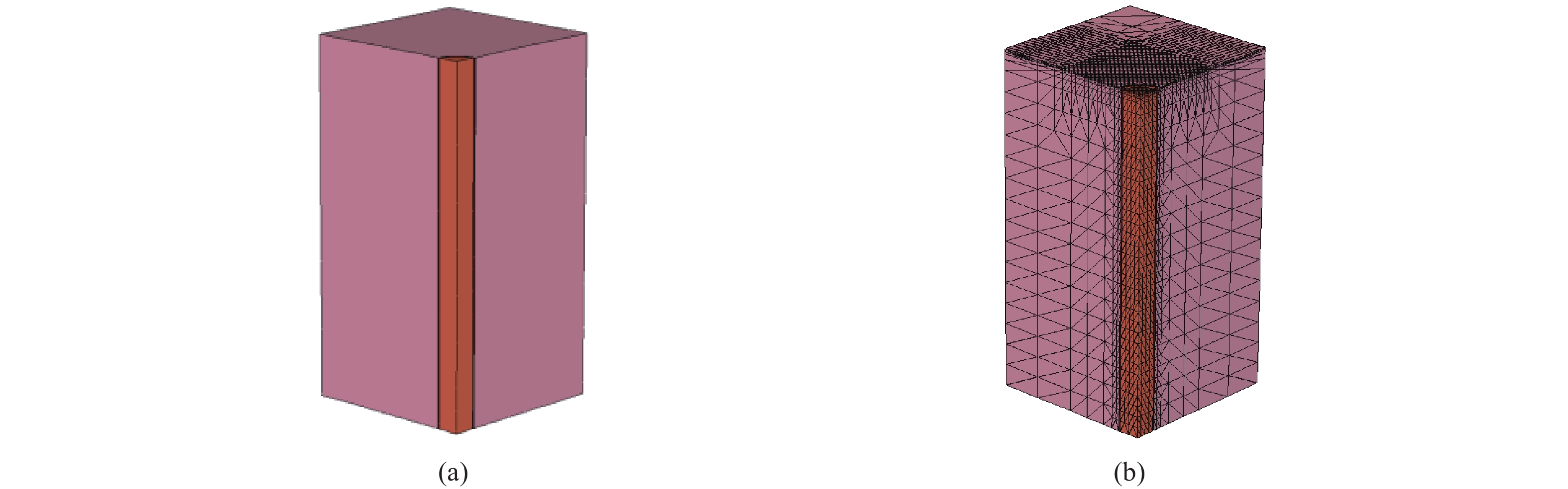
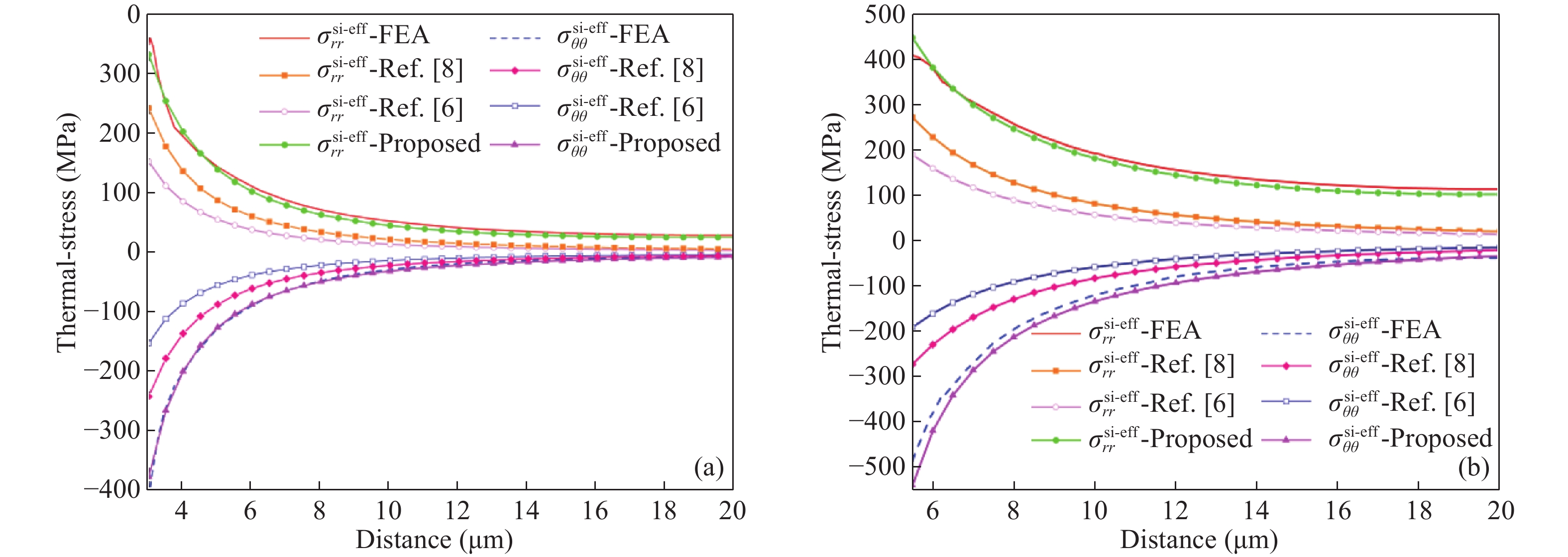
Table 1. The parameters involved in the TCAD simulation.
| Name | Description | Value | ||
| υCu | Poisson’s ratio of Cu | 0.343 | ||
| αCu | CTE of Cu (ppm/°C) | 17.7 | ||
| ECu | Young’s module of Cu (GPa) | 115.5 | ||
υ


|
Poisson’s ratio of SiO2 | 0.16 | ||
α


|
CTE of SiO2 (ppm/°C) | 0.51 | ||
E


|
Young’s module of SiO2 (GPa) | 71.7 | ||
| υsi | Poisson’s ratio of Si | 0.28 | ||
| αsi | CTE of Si (ppm/°C) | 3.05 | ||
| Cij | Stiffness of silicon with orthotropic material property (GPa) | C11 = 165, C12 = 63.9, C44 = 79.6 | ||
| a | Radius of TSV (μm) | 2.5 or 5 | ||
| b-a | Thickness of insulation layer | 0.5 | ||
| ΔT | Temperature load (°C) | ?225 |
 DownLoad: CSV
| [1] |
Waldrop M M. More than Moore. Nature, 2016, 530(7589): 144 doi: 10.1038/530144a
|
| [2] |
Shen W W, Chen K N. Three-dimensional integrated circuit (3D IC) key technology: through-silicon via (TSV). Nanoscale Res Lett, 2017, 12(1): 56 doi: 10.1186/s11671-017-1831-4
|
| [3] |
Tsai H Y, Kuo C W. Thermal stress and failure location analysis for through silicon via in 3D integration. J Mechan, 2016, 32(01): 47
|
| [4] |
Johnson R W, Shen Y L. Analysis of thermal stress and its influence on carrier mobility in three-dimensional microelectronic chip stack. J Electron Pack, 2015, 137(2): 021011 doi: 10.1115/1.4029345
|
| [5] |
Ryu S K, Zhao Q, Hecker M, et al. Micro-Raman spectroscopy and analysis of near-surface stresses in silicon around through-silicon vias for three-dimensional interconnects. J Appl Phys, 2012, 111(6): 063513 doi: 10.1063/1.3696980
|
| [6] |
Athikulwongse K, Yang J S, Pan D Z, et al. Impact of mechanical stress on the full chip timing for through-silicon-via-based 3-D ICs. IEEE Trans Comput-Aid Des Integr Circuits Syst, 2013, 32(6): 905 doi: 10.1109/TCAD.2013.2237770
|
| [7] |
Chen C. Characterization of in-plane stress in TSV array—a unit model approach. Proceed IEEE, 2014: 2020
|
| [8] |
Marella S K, Sapatnekar S S. A holistic analysis of circuit performance variations in 3-D ICs with thermal and TSV-induced stress considerations. IEEE Trans Very Large Scale Integr (VLSI) Syst, 2015, 23(7): 1308 doi: 10.1109/TVLSI.2014.2335154
|
| [9] |
Li Y, Pan D Z. An accurate semi-analytical framework for full-chip TSV-induced stress modeling. Proceedings of the 50th ACM ADAC, 2013: 181
|
| [10] |
McDonough C, Backes B, Wang W, et al. Thermal and spatial profiling of TSV-induced stress in 3DICs. Proc IEEE, 2011: 5D.2.1
|
| [11] |
Jung M, Mitra J, Pan D Z, et al. TSV stress-aware full-chip mechanical reliability analysis and optimization for 3D IC. Commun ACM, 2014, 57(1): 107 doi: 10.1145/2541883
|
| [12] |
Roh M H, Sharma A, Lee J H, et al. Extrusion suppression of TSV filling metal by Cu-W electroplating for three-dimensional microelectronic packaging. Metallurg Mater Transa A, 2015, 46(5): 2051 doi: 10.1007/s11661-015-2801-z
|
| [13] |
Timoshenko S P, Goodier J N. Theory of elasticity. New York: McGraw-Hill, 1951
|
| [14] |
Lekhnitskii S G. Anisotropic plates. New York: Science Publishers, Inc., 1968
|
| [15] |
Chiang C R. Thermal mismatch stress of a cylindrical inclusion in a cubic crystal. Eng Fract Mechan, 2008, 75(8): 2295 doi: 10.1016/j.engfracmech.2007.09.002
|
| [16] |
Lekhnitskij, S. G. Theory of the elasticity of anisotropic bodies. 1977
|
| [17] |
Interconnect T S. Manual and user guide. Synopsys, Inc, 2014
|


Article views: 4246 Times PDF downloads: 79 Times Cited by: 0 Times
Received: 14 May 2017 Revised: 17 July 2017 Online: Uncorrected proof: 24 January 2018Accepted Manuscript: 02 February 2018Published: 02 February 2018
| Citation: |
Song Liu, Guangbao Shan. An anisotropic thermal-stress model for through-silicon via[J]. Journal of Semiconductors, 2018, 39(2): 026003. doi: 10.1088/1674-4926/39/2/026003
****
S Liu, G B Shan. An anisotropic thermal-stress model for through-silicon via[J]. J. Semicond., 2018, 39(2): 026003. doi: 10.1088/1674-4926/39/2/026003.

|
Project supported by the Aerospace Advanced Manufacturing Technology Research Joint Fund (No. U1537208).
| [1] |
Waldrop M M. More than Moore. Nature, 2016, 530(7589): 144 doi: 10.1038/530144a
|
| [2] |
Shen W W, Chen K N. Three-dimensional integrated circuit (3D IC) key technology: through-silicon via (TSV). Nanoscale Res Lett, 2017, 12(1): 56 doi: 10.1186/s11671-017-1831-4
|
| [3] |
Tsai H Y, Kuo C W. Thermal stress and failure location analysis for through silicon via in 3D integration. J Mechan, 2016, 32(01): 47
|
| [4] |
Johnson R W, Shen Y L. Analysis of thermal stress and its influence on carrier mobility in three-dimensional microelectronic chip stack. J Electron Pack, 2015, 137(2): 021011 doi: 10.1115/1.4029345
|
| [5] |
Ryu S K, Zhao Q, Hecker M, et al. Micro-Raman spectroscopy and analysis of near-surface stresses in silicon around through-silicon vias for three-dimensional interconnects. J Appl Phys, 2012, 111(6): 063513 doi: 10.1063/1.3696980
|
| [6] |
Athikulwongse K, Yang J S, Pan D Z, et al. Impact of mechanical stress on the full chip timing for through-silicon-via-based 3-D ICs. IEEE Trans Comput-Aid Des Integr Circuits Syst, 2013, 32(6): 905 doi: 10.1109/TCAD.2013.2237770
|
| [7] |
Chen C. Characterization of in-plane stress in TSV array—a unit model approach. Proceed IEEE, 2014: 2020
|
| [8] |
Marella S K, Sapatnekar S S. A holistic analysis of circuit performance variations in 3-D ICs with thermal and TSV-induced stress considerations. IEEE Trans Very Large Scale Integr (VLSI) Syst, 2015, 23(7): 1308 doi: 10.1109/TVLSI.2014.2335154
|
| [9] |
Li Y, Pan D Z. An accurate semi-analytical framework for full-chip TSV-induced stress modeling. Proceedings of the 50th ACM ADAC, 2013: 181
|
| [10] |
McDonough C, Backes B, Wang W, et al. Thermal and spatial profiling of TSV-induced stress in 3DICs. Proc IEEE, 2011: 5D.2.1
|
| [11] |
Jung M, Mitra J, Pan D Z, et al. TSV stress-aware full-chip mechanical reliability analysis and optimization for 3D IC. Commun ACM, 2014, 57(1): 107 doi: 10.1145/2541883
|
| [12] |
Roh M H, Sharma A, Lee J H, et al. Extrusion suppression of TSV filling metal by Cu-W electroplating for three-dimensional microelectronic packaging. Metallurg Mater Transa A, 2015, 46(5): 2051 doi: 10.1007/s11661-015-2801-z
|
| [13] |
Timoshenko S P, Goodier J N. Theory of elasticity. New York: McGraw-Hill, 1951
|
| [14] |
Lekhnitskii S G. Anisotropic plates. New York: Science Publishers, Inc., 1968
|
| [15] |
Chiang C R. Thermal mismatch stress of a cylindrical inclusion in a cubic crystal. Eng Fract Mechan, 2008, 75(8): 2295 doi: 10.1016/j.engfracmech.2007.09.002
|
| [16] |
Lekhnitskij, S. G. Theory of the elasticity of anisotropic bodies. 1977
|
| [17] |
Interconnect T S. Manual and user guide. Synopsys, Inc, 2014
|

 WeChat ID
Journal of Semiconductors © 2017 All Rights Reserved 京ICP備05085259號(hào)-2


