


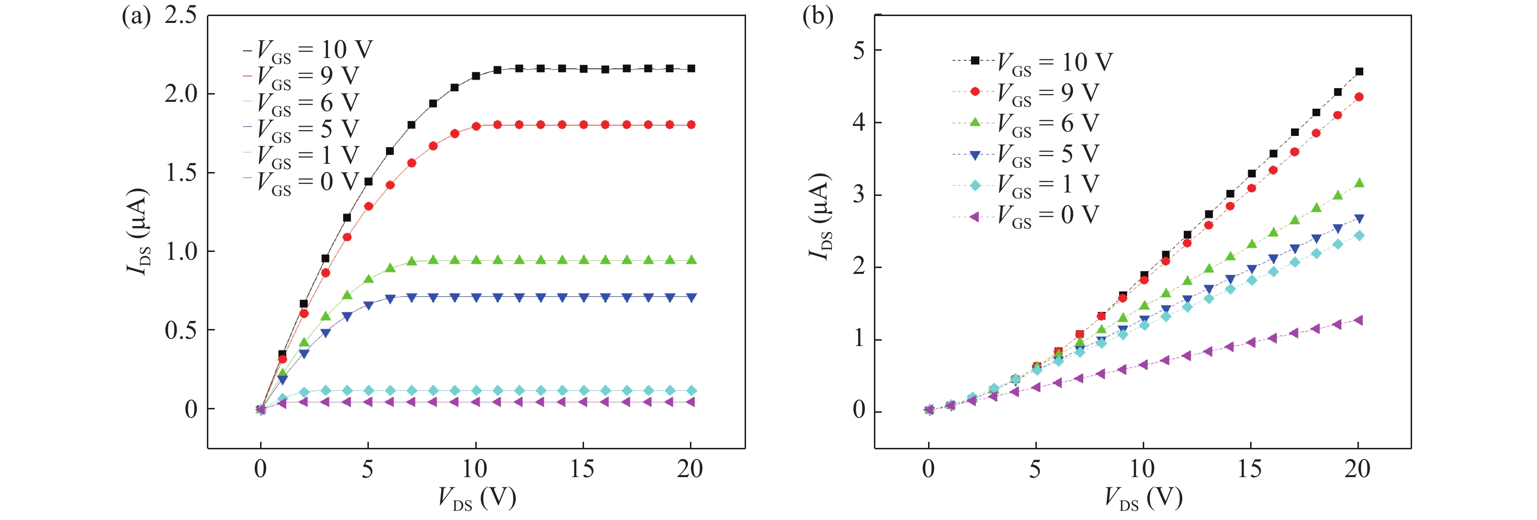
Fig. 1.
(Color online) DC characteristics of IGZO TFT. (a) Output characteristics. (b) Transfer characteristics.
SEMICONDUCTOR PHYSICS
G K Dayananda1, , C Shantharama Rai2, A Jayarama3 and Hyun Jae Kim4
Corresponding author: G K Dayananda, Email: dayanand.gk@gmail.com
Abstract: An efficient drain current simulation model for the electron irradiation effect on the electrical parameters of amorphous In–Ga–Zn–O (IGZO) thin-film transistors is developed. The model is developed based on the specifications such as gate capacitance, channel length, channel width, flat band voltage etc. Electrical parameters of un-irradiated IGZO samples were simulated and compared with the experimental parameters and 1 kGy electron irradiated parameters. The effect of electron irradiation on the IGZO sample was analysed by developing a mathematical model.
Key words: simulation model, IGZO, TFT, electron irradiation
| [1] |
Kamiya T, Nomura K, Hosono H. Present status of amorphous IGZO thin-film transistors. Sci Technol Adv Mater, 2015, 11(4): 044305
|
| [2] |
Ito M, Kon M, Miyazaki C, et al. Amorphous oxide TFT and their applications in electrophoretic displays. Phys Status Solidi, 2008, 205(8): 1885 doi: 10.1002/pssa.v205:8
|
| [3] |
Jeong J K, Jeong J H, Yang H W, et al. High performance thin film transistors with co-sputtered amorphous indium gallium zinc oxide channel. Appl Phys Lett, 2007, 91: 113505 doi: 10.1063/1.2783961
|
| [4] |
Kumomi H, Nomura K, Kamiya T, et al. Amorphous oxide channel TFTs. Thin Solid Films, 2007, 516(7): 1516
|
| [5] |
Hsieh H H, Kamiya T, Nomura K, et al. Modeling of amorphous InGaZnO4 thin film transistors and their subgap density of states. Jpn Appl Phys Lett, 2008, 92: 133503 doi: 10.1063/1.2857463
|
| [6] |
Fung T C, Chuang C S, Chen C, et al. Two-dimensional numerical simulation of radio frequency sputter amorphous In–Ga–Zn–O thin-film transistors. J Appl Phys, 2009, 106: 084511 doi: 10.1063/1.3234400
|
| [7] |
Park J H, Lee S, Jeon K, et al. Density of states-based DC I–V model of amorphous gallium–indium–zinc–oxide thin-film transistors. IEEE Electron Device Lett, 2009, 30(10): 1069 doi: 10.1109/LED.2009.2028042
|
| [8] |
Short K, Buren D. Printable spacecraft: flexible electronics platforms for NASA mission’s. NASA Innovative Advanced Concepts (NAIC), Phase 2 Final Report Printable Spacecraft, September 2014
|
| [9] |
Rafí J M, Campabadal F, Ohyama H, et al. 2 MeV electron irradiation effects on the electrical characteristics of metal–oxide–silicon capacitors with atomic layer deposited Al2O3, HfO2 and nanolaminated dielectrics. Solid-State Electron, 2013, 79: 65 doi: 10.1016/j.sse.2012.06.011
|
| [10] |
Indluru A, Holbert K E, Alford T L. Gamma radiation effects on indium–zinc oxide thin-film transistors. Thin Solid Films, 2013, 539: 342 doi: 10.1016/j.tsf.2013.04.148
|
| [11] |
Cramer T, Sacchetti A, Lobato M T, et al. Radiation-tolerant flexible large-area electronics based on oxide semiconductors. Adv Electron Mater, 2016, 2: 1500489 doi: 10.1002/aelm.v2.7
|
| [12] |
Liu Y, Wu W, En Y, et al. Total dose ionizing radiation effects in the indium–zinc oxide thin-film transistors. IEEE Electron Device Lett, 2014, 35(3): 369 doi: 10.1109/LED.2014.2301801
|
| [13] |
Kim H J. International collaboration for advanced AMOLED. ICAA Koranet Annual Conference, South Korea, 2010
|
| [14] |
Siddappa K, Ganesh, Balakrishna K M, et al. Variable energy microtron for R and D work. Radiat Phys Chem, 1998, 51(4–6): 441 doi: 10.1016/S0969-806X(97)00165-5
|
| [15] |
Stoenescu G, Iacobescu G. Fast electron irradiation effects on MOS transistor microscopic parameters—experimental data and theoretical models. J Optoelectron Adv Mater, 2005, 7: 1629
|

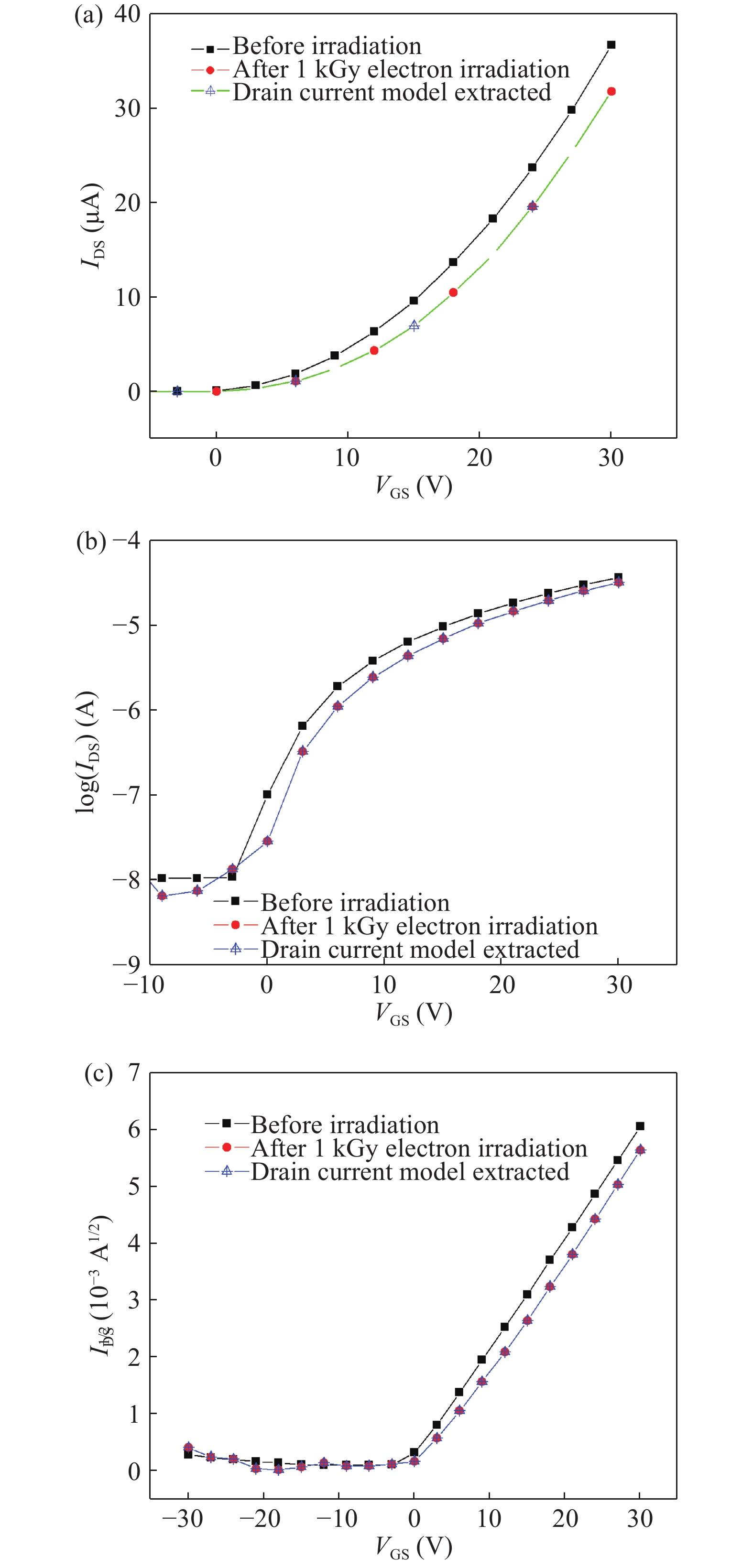
Table 1. Comparison of different parameter values for both simulated and IGZO TFT values.
| Parameter | SS (V/Decade) | μsat (cm2/(V·s)) | Ion/Ioff | Vth (V) | ||
| Simulated value | 1.40 | 0.976 | 1.4 × 10⁴ | ?3.51 | ||
| IGZO TFT value | 1.38 | 0.853 | 1.36 × 10⁴ | ?3.47 |
 DownLoad: CSV
Table 2. Effect of electron irradiation on different TFT parameters.
| Parameter | SS (V/Decade) | μsat (cm2/(V·s)) | Ion/Ioff | Vth (V) | ||
| Before irradiation | 3.058749 | 0.312153 | 4326.254 | ?3.8 | ||
| After 1 kGy irradiation | 3.511243 | 0.29967 | 6899.364 | ?1.4 |
DownLoad: CSV
| [1] |
Kamiya T, Nomura K, Hosono H. Present status of amorphous IGZO thin-film transistors. Sci Technol Adv Mater, 2015, 11(4): 044305
|
| [2] |
Ito M, Kon M, Miyazaki C, et al. Amorphous oxide TFT and their applications in electrophoretic displays. Phys Status Solidi, 2008, 205(8): 1885 doi: 10.1002/pssa.v205:8
|
| [3] |
Jeong J K, Jeong J H, Yang H W, et al. High performance thin film transistors with co-sputtered amorphous indium gallium zinc oxide channel. Appl Phys Lett, 2007, 91: 113505 doi: 10.1063/1.2783961
|
| [4] |
Kumomi H, Nomura K, Kamiya T, et al. Amorphous oxide channel TFTs. Thin Solid Films, 2007, 516(7): 1516
|
| [5] |
Hsieh H H, Kamiya T, Nomura K, et al. Modeling of amorphous InGaZnO4 thin film transistors and their subgap density of states. Jpn Appl Phys Lett, 2008, 92: 133503 doi: 10.1063/1.2857463
|
| [6] |
Fung T C, Chuang C S, Chen C, et al. Two-dimensional numerical simulation of radio frequency sputter amorphous In–Ga–Zn–O thin-film transistors. J Appl Phys, 2009, 106: 084511 doi: 10.1063/1.3234400
|
| [7] |
Park J H, Lee S, Jeon K, et al. Density of states-based DC I–V model of amorphous gallium–indium–zinc–oxide thin-film transistors. IEEE Electron Device Lett, 2009, 30(10): 1069 doi: 10.1109/LED.2009.2028042
|
| [8] |
Short K, Buren D. Printable spacecraft: flexible electronics platforms for NASA mission’s. NASA Innovative Advanced Concepts (NAIC), Phase 2 Final Report Printable Spacecraft, September 2014
|
| [9] |
Rafí J M, Campabadal F, Ohyama H, et al. 2 MeV electron irradiation effects on the electrical characteristics of metal–oxide–silicon capacitors with atomic layer deposited Al2O3, HfO2 and nanolaminated dielectrics. Solid-State Electron, 2013, 79: 65 doi: 10.1016/j.sse.2012.06.011
|
| [10] |
Indluru A, Holbert K E, Alford T L. Gamma radiation effects on indium–zinc oxide thin-film transistors. Thin Solid Films, 2013, 539: 342 doi: 10.1016/j.tsf.2013.04.148
|
| [11] |
Cramer T, Sacchetti A, Lobato M T, et al. Radiation-tolerant flexible large-area electronics based on oxide semiconductors. Adv Electron Mater, 2016, 2: 1500489 doi: 10.1002/aelm.v2.7
|
| [12] |
Liu Y, Wu W, En Y, et al. Total dose ionizing radiation effects in the indium–zinc oxide thin-film transistors. IEEE Electron Device Lett, 2014, 35(3): 369 doi: 10.1109/LED.2014.2301801
|
| [13] |
Kim H J. International collaboration for advanced AMOLED. ICAA Koranet Annual Conference, South Korea, 2010
|
| [14] |
Siddappa K, Ganesh, Balakrishna K M, et al. Variable energy microtron for R and D work. Radiat Phys Chem, 1998, 51(4–6): 441 doi: 10.1016/S0969-806X(97)00165-5
|
| [15] |
Stoenescu G, Iacobescu G. Fast electron irradiation effects on MOS transistor microscopic parameters—experimental data and theoretical models. J Optoelectron Adv Mater, 2005, 7: 1629
|


Article views: 5024 Times PDF downloads: 108 Times Cited by: 0 Times
Received: 18 April 2017 Revised: 02 August 2017 Online: Uncorrected proof: 24 January 2018Accepted Manuscript: 02 February 2018Published: 02 February 2018
| Citation: |
G K Dayananda, C Shantharama Rai, A Jayarama, Hyun Jae Kim. Simulation model for electron irradiated IGZO thin film transistors[J]. Journal of Semiconductors, 2018, 39(2): 022002. doi: 10.1088/1674-4926/39/2/022002
****
G K Dayananda, C S Rai, A Jayarama, H J Kim. Simulation model for electron irradiated IGZO thin film transistors[J]. J. Semicond., 2018, 39(2): 022002. doi: 10.1088/1674-4926/39/2/022002.

|
| [1] |
Kamiya T, Nomura K, Hosono H. Present status of amorphous IGZO thin-film transistors. Sci Technol Adv Mater, 2015, 11(4): 044305
|
| [2] |
Ito M, Kon M, Miyazaki C, et al. Amorphous oxide TFT and their applications in electrophoretic displays. Phys Status Solidi, 2008, 205(8): 1885 doi: 10.1002/pssa.v205:8
|
| [3] |
Jeong J K, Jeong J H, Yang H W, et al. High performance thin film transistors with co-sputtered amorphous indium gallium zinc oxide channel. Appl Phys Lett, 2007, 91: 113505 doi: 10.1063/1.2783961
|
| [4] |
Kumomi H, Nomura K, Kamiya T, et al. Amorphous oxide channel TFTs. Thin Solid Films, 2007, 516(7): 1516
|
| [5] |
Hsieh H H, Kamiya T, Nomura K, et al. Modeling of amorphous InGaZnO4 thin film transistors and their subgap density of states. Jpn Appl Phys Lett, 2008, 92: 133503 doi: 10.1063/1.2857463
|
| [6] |
Fung T C, Chuang C S, Chen C, et al. Two-dimensional numerical simulation of radio frequency sputter amorphous In–Ga–Zn–O thin-film transistors. J Appl Phys, 2009, 106: 084511 doi: 10.1063/1.3234400
|
| [7] |
Park J H, Lee S, Jeon K, et al. Density of states-based DC I–V model of amorphous gallium–indium–zinc–oxide thin-film transistors. IEEE Electron Device Lett, 2009, 30(10): 1069 doi: 10.1109/LED.2009.2028042
|
| [8] |
Short K, Buren D. Printable spacecraft: flexible electronics platforms for NASA mission’s. NASA Innovative Advanced Concepts (NAIC), Phase 2 Final Report Printable Spacecraft, September 2014
|
| [9] |
Rafí J M, Campabadal F, Ohyama H, et al. 2 MeV electron irradiation effects on the electrical characteristics of metal–oxide–silicon capacitors with atomic layer deposited Al2O3, HfO2 and nanolaminated dielectrics. Solid-State Electron, 2013, 79: 65 doi: 10.1016/j.sse.2012.06.011
|
| [10] |
Indluru A, Holbert K E, Alford T L. Gamma radiation effects on indium–zinc oxide thin-film transistors. Thin Solid Films, 2013, 539: 342 doi: 10.1016/j.tsf.2013.04.148
|
| [11] |
Cramer T, Sacchetti A, Lobato M T, et al. Radiation-tolerant flexible large-area electronics based on oxide semiconductors. Adv Electron Mater, 2016, 2: 1500489 doi: 10.1002/aelm.v2.7
|
| [12] |
Liu Y, Wu W, En Y, et al. Total dose ionizing radiation effects in the indium–zinc oxide thin-film transistors. IEEE Electron Device Lett, 2014, 35(3): 369 doi: 10.1109/LED.2014.2301801
|
| [13] |
Kim H J. International collaboration for advanced AMOLED. ICAA Koranet Annual Conference, South Korea, 2010
|
| [14] |
Siddappa K, Ganesh, Balakrishna K M, et al. Variable energy microtron for R and D work. Radiat Phys Chem, 1998, 51(4–6): 441 doi: 10.1016/S0969-806X(97)00165-5
|
| [15] |
Stoenescu G, Iacobescu G. Fast electron irradiation effects on MOS transistor microscopic parameters—experimental data and theoretical models. J Optoelectron Adv Mater, 2005, 7: 1629
|

 WeChat ID
Journal of Semiconductors © 2017 All Rights Reserved 京ICP備05085259號-2


