


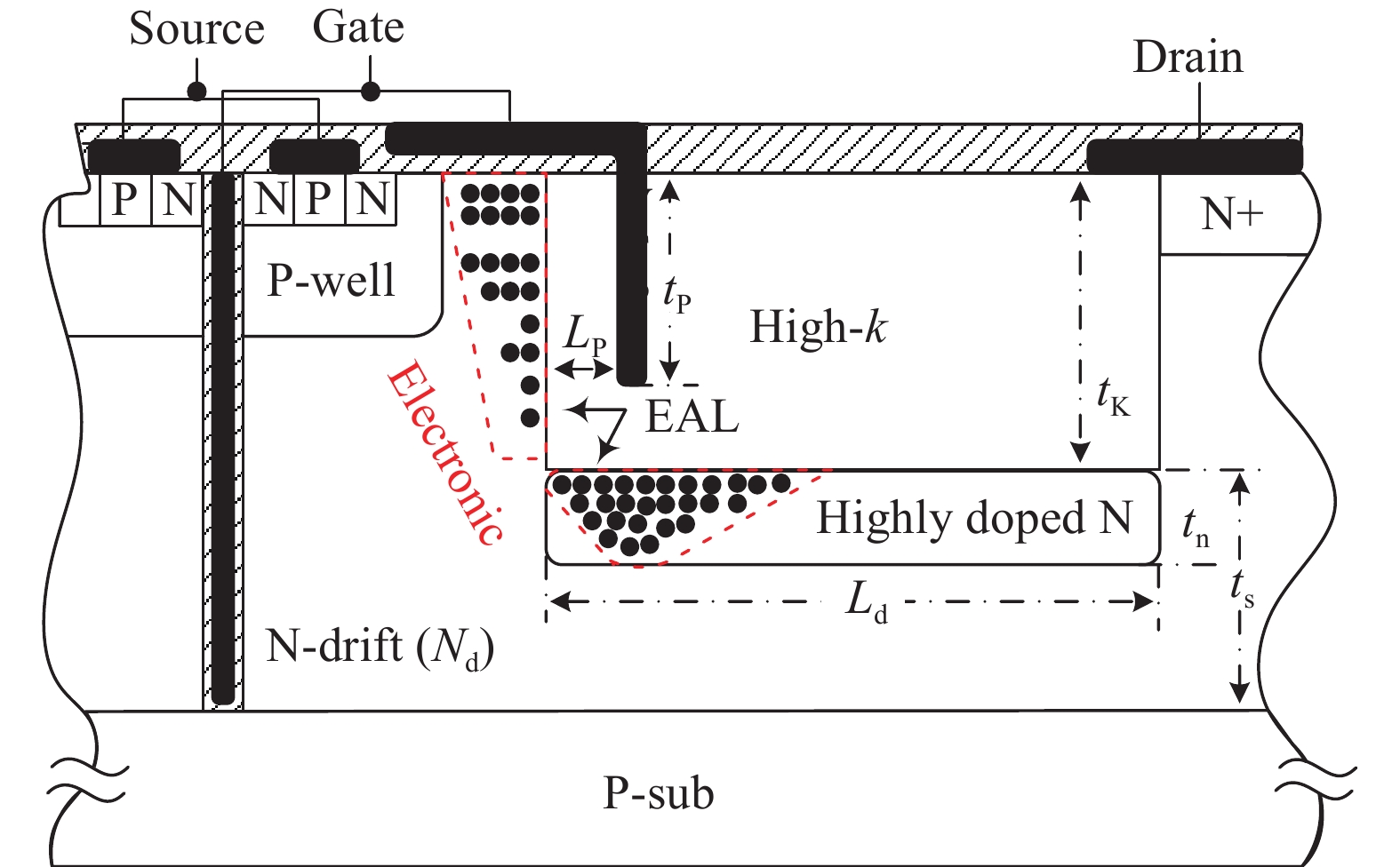
Fig. 1.
(Color?online) Schematic cross-section view of VFP HK LDMOS.
SEMICONDUCTOR DEVICES
Lijuan Wu, Limin Hu, Lin Zhu, Hang Yang, Bing Lei and Haiqing Xie
Corresponding author: Lijuan Wu, 305719669@qq.com
Abstract: An ultralow specific on-resistance high-k LDMOS with vertical field plate (VFP HK LDMOS) is proposed. The high-k dielectric trench and highly doped interface N+ layer are made in bulk silicon to reduce the surface field of the drift region in the VFP HK LDMOS. The gate vertical field plate (VFP) pinning in the high-k dielectric trench can modulate the bulk electric field. The high-k dielectric not only provides polarized charges to assist depletion of the drift region, so that the drift region and high-k trench maintain charge balance adaptively, but also can fully assist in depleting the drift region to increase the drift doping concentration and reshape the electric field to avoid premature breakdown. Compared with the conventional structure, the VFP HK LDMOS has the breakdown voltage of 629.1 V at the drift length of 40 μm and the specific on-resistance of 38.4 mΩ·cm2 at the gate potential of 15 V. Then the power figure of merit is 10.31 MW/cm2.
Key words: high-k dielectric, vertical field plate, high voltage, specific on-resistance, polarized charges
| [1] |
Hu S D, Zhang B, Li Z J, et al. A new structure and its analytical model for the vertical interface electric field of a partial-SOI high voltage device. Chin Phys B, 2010, 19(3): 037303 doi: 10.1088/1674-1056/19/3/037303
|
| [2] |
Hu S D, Zhang B, Li Z J. A new analytical model of high voltage silicon on insulator(SOI) thin film devices. Chin Phys B, 2009, 18(1): 315 doi: 10.1088/1674-1056/18/1/051
|
| [3] |
Li Q, Li Z J, Zhang B. Analytical model for the surface electrical field distribution of double RESURF device with surface. Acta Phys Soc, 2007, 56(11): 6660
|
| [4] |
Zhou K, Luo X, Xu Q, et al. A RESURF-enhanced p-channel trench SOI LDMOS with ultralow specific on-resistance. IEEE Trans Electron Devices, 2014, 61(7): 2466 doi: 10.1109/TED.2014.2321146
|
| [5] |
Wu L J, Zhang W T, Qiao M, et al. SOI SJ high voltage device with linear variable doping interface thin silicon layer. Electron Lett, 2012, 48(5): 297
|
| [6] |
Zhang W, Zhang B, Qiao M, et al. Optimization and new structure of superjunction with isolator layer. IEEE Trans Electron Devices, 2016, 64(1): 217
|
| [7] |
Li J, Li P, Huo W, et al. Analysis and fabrication of an LDMOS with high-permittivity dielectric. IEEE Electron Device Letters, 2011, 32(9): 1266 doi: 10.1109/LED.2011.2158383
|
| [8] |
Luo X, Jiang Y H, Zhou K, et al. Ultralow specific on-resistance superjunction vertical DMOS with high-k, dielectric pillar. IEEE Electron Device Lett, 2012, 33(7): 1042 doi: 10.1109/LED.2012.2196969
|
| [9] |
Chen X B, Huang M M. A Vertical power MOSFET with an interdigitated drift region using high-k insulator. IEEE Trans Electron Devices, 2012, 59(9): 2430 doi: 10.1109/TED.2012.2204890
|
| [10] |
Chen X. Super-junction voltage sustaining layer with alternating semiconductor and high-k dielectric regions: US Patent, US7230310. 2007
|
| [11] |
Guo Y, Yao J, Zhang B, et al. Variation of lateral width technique in SoI high-voltage lateral `double-diffused` metal–oxide–semiconductor transistors using high-k dielectric. IEEE Electron Device Lett, 2015, 36(3): 262 doi: 10.1109/LED.2015.2393913
|
| [12] |
Li H, Chen X B. Deep trench junction termination employing variable-k dielectric for high voltage devices. IEEE 11th International Conference on ASIC (ASICON), Chengdu, China, 2015
|
| [13] |
Luo X, Lv M, Yin C, et al. Ultralow on-resistance SOI LDMOS with three separated gates and high-k, dielectric. IEEE Trans Electron Devices, 2016, 63(9): 3804 doi: 10.1109/TED.2016.2589322
|
| [14] |
Wu L, Zhang W, Shi Q, et al. Trench SOI LDMOS with vertical field plate. Electron Lett, 2014, 50(25): 1982 doi: 10.1049/el.2014.3443
|
| [15] |
Xia C, Cheng X, Wang Z, et al. Improvement of SOI trench LDMOS performance with double vertical metal field plate. IEEE Trans Electron Devices, 2014, 61(10): 3477 doi: 10.1109/TED.2014.2349553
|
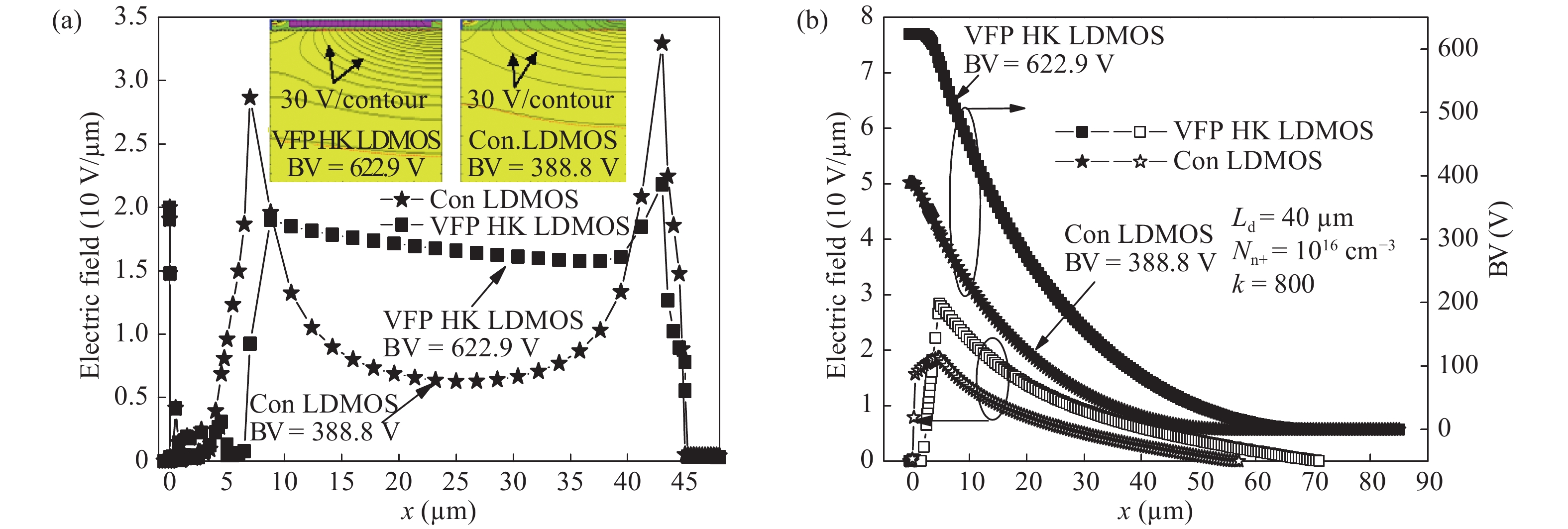
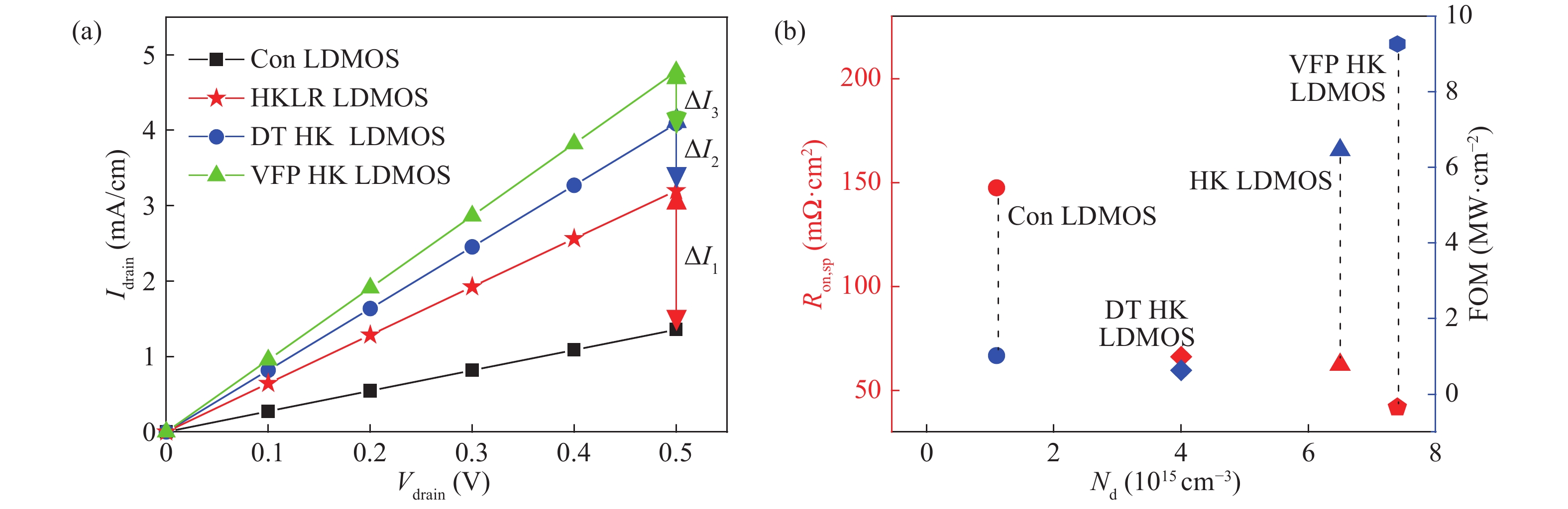
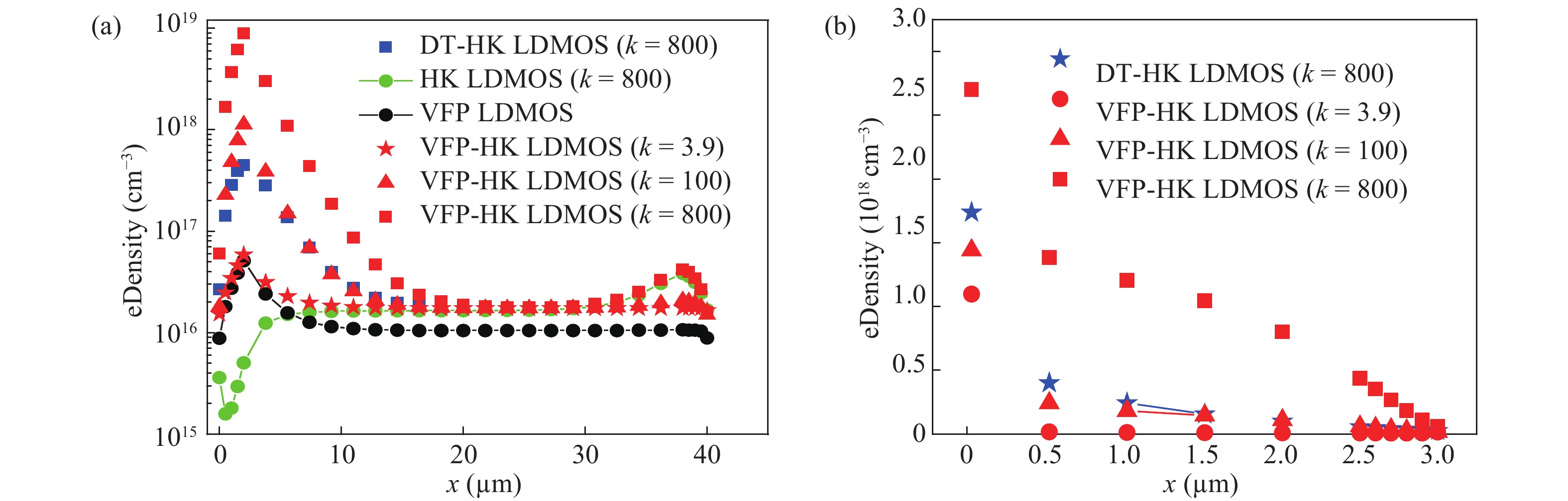
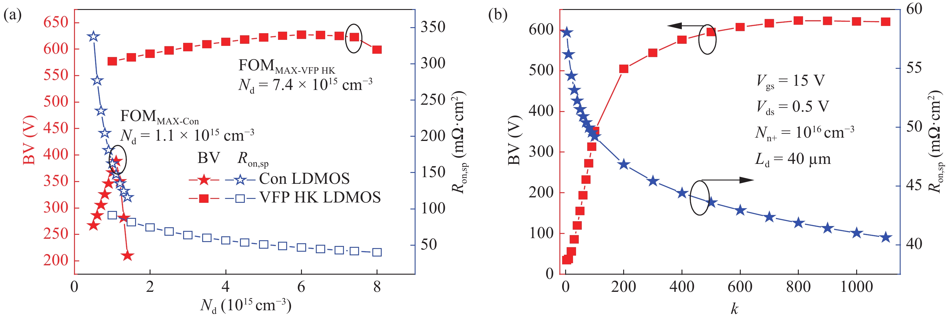
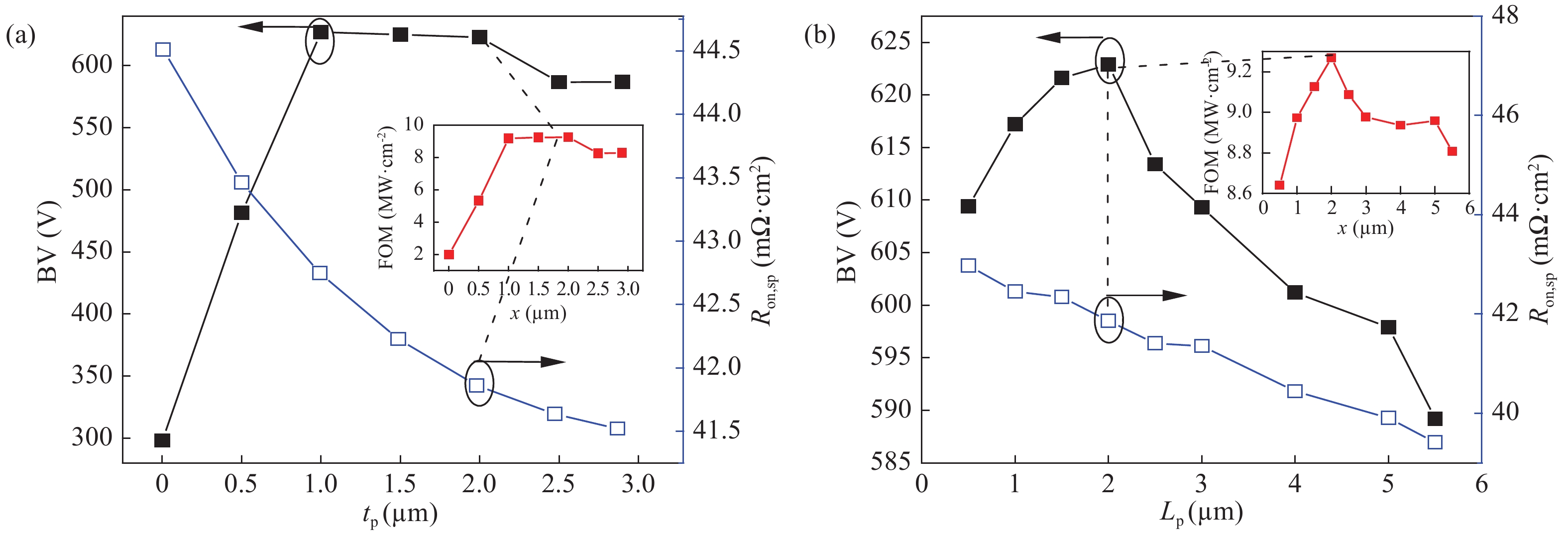
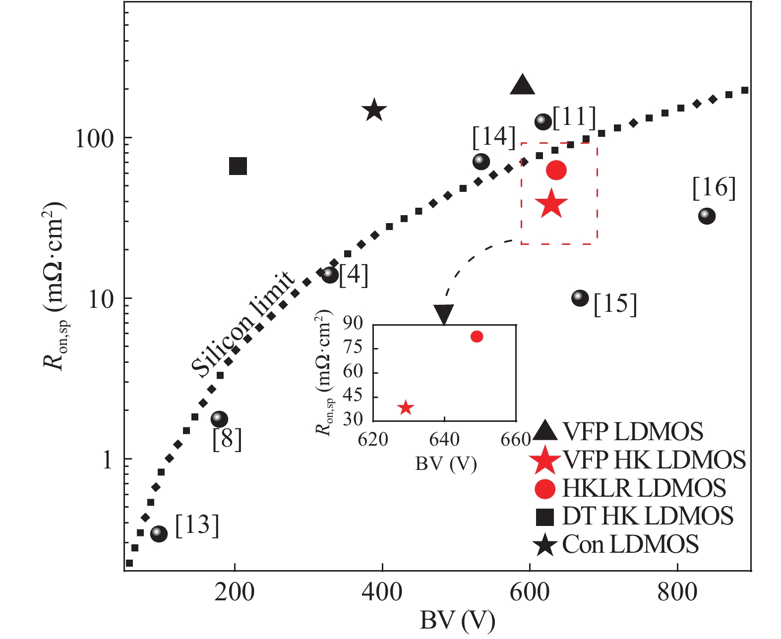
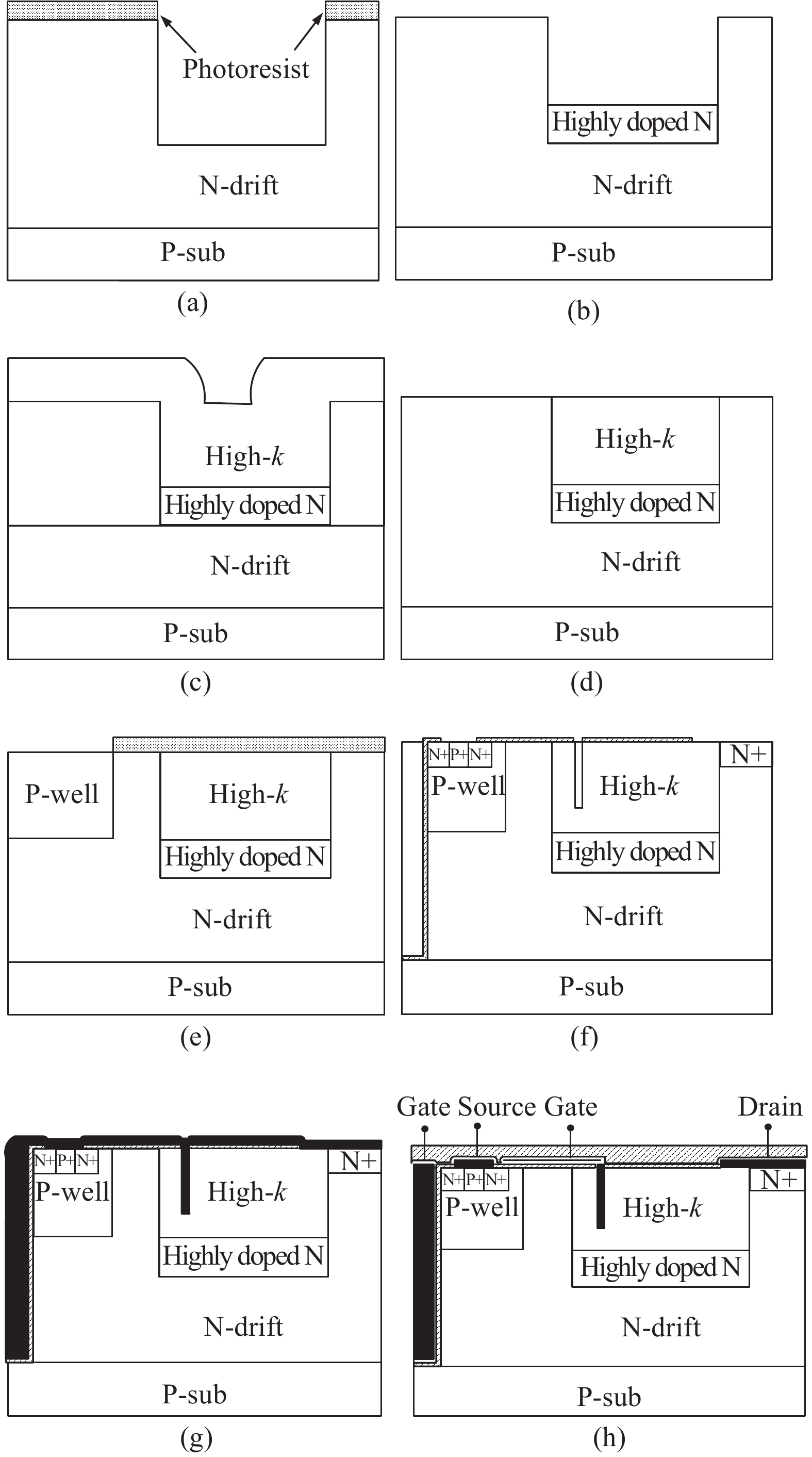
Table 2. BV, Ron,sp, FOM = BV2/Ron,sp for the devices.
| Device structure | Nd (1015 cm?3) | BV (V) | Ron,sp (mΩ·cm2) @ Vgs = 15 V | BV2/Ron,sp (MW/cm2) |
| VFP HK LDMOS (k = 800) | 7.5 | 629.1 | 38.4 | 10.31 |
| HKLR LDMOS (k = 800)[14] | 3.5 | 649 | 82.8 | 5.09 |
| DT HK LDMOS (lp = 2k = 800) | 2 | 162.4 | 86.4 | 0.31 |
| Con. LDMOS | 1.1 | 388.9 | 147.5 | 1.02 |
 DownLoad: CSV
Table 1. Structure parameters used in the simulation.
| Symbol | Description | Value |
| tp | Length of gate field plate (μm) | 2 |
| tk | Depth of high-k trench (μm) | 3 |
| k | k value of high-k dielectric | 800 |
| Ld | Length of N (μm) | Optimized |
| Nn+ | Concentration of N (cm?3) | Optimized |
| tn | Thickness of N (μm) | 0.5 |
| ts | Distance from the bottom of the high-k trench to the top of the substrate (μm) | 2 |
| Lp | Distance from vertical field plate to the left side of the high-k trench (μm) | 2 |
| Nd | Concentration of drift region (cm?3) | 7.4


|
| tsub | Thickness of substrate (μm) | 80 |
| Nsub | Concentration of substrate (cm?3) | 1


|
DownLoad: CSV
| [1] |
Hu S D, Zhang B, Li Z J, et al. A new structure and its analytical model for the vertical interface electric field of a partial-SOI high voltage device. Chin Phys B, 2010, 19(3): 037303 doi: 10.1088/1674-1056/19/3/037303
|
| [2] |
Hu S D, Zhang B, Li Z J. A new analytical model of high voltage silicon on insulator(SOI) thin film devices. Chin Phys B, 2009, 18(1): 315 doi: 10.1088/1674-1056/18/1/051
|
| [3] |
Li Q, Li Z J, Zhang B. Analytical model for the surface electrical field distribution of double RESURF device with surface. Acta Phys Soc, 2007, 56(11): 6660
|
| [4] |
Zhou K, Luo X, Xu Q, et al. A RESURF-enhanced p-channel trench SOI LDMOS with ultralow specific on-resistance. IEEE Trans Electron Devices, 2014, 61(7): 2466 doi: 10.1109/TED.2014.2321146
|
| [5] |
Wu L J, Zhang W T, Qiao M, et al. SOI SJ high voltage device with linear variable doping interface thin silicon layer. Electron Lett, 2012, 48(5): 297
|
| [6] |
Zhang W, Zhang B, Qiao M, et al. Optimization and new structure of superjunction with isolator layer. IEEE Trans Electron Devices, 2016, 64(1): 217
|
| [7] |
Li J, Li P, Huo W, et al. Analysis and fabrication of an LDMOS with high-permittivity dielectric. IEEE Electron Device Letters, 2011, 32(9): 1266 doi: 10.1109/LED.2011.2158383
|
| [8] |
Luo X, Jiang Y H, Zhou K, et al. Ultralow specific on-resistance superjunction vertical DMOS with high-k, dielectric pillar. IEEE Electron Device Lett, 2012, 33(7): 1042 doi: 10.1109/LED.2012.2196969
|
| [9] |
Chen X B, Huang M M. A Vertical power MOSFET with an interdigitated drift region using high-k insulator. IEEE Trans Electron Devices, 2012, 59(9): 2430 doi: 10.1109/TED.2012.2204890
|
| [10] |
Chen X. Super-junction voltage sustaining layer with alternating semiconductor and high-k dielectric regions: US Patent, US7230310. 2007
|
| [11] |
Guo Y, Yao J, Zhang B, et al. Variation of lateral width technique in SoI high-voltage lateral `double-diffused` metal–oxide–semiconductor transistors using high-k dielectric. IEEE Electron Device Lett, 2015, 36(3): 262 doi: 10.1109/LED.2015.2393913
|
| [12] |
Li H, Chen X B. Deep trench junction termination employing variable-k dielectric for high voltage devices. IEEE 11th International Conference on ASIC (ASICON), Chengdu, China, 2015
|
| [13] |
Luo X, Lv M, Yin C, et al. Ultralow on-resistance SOI LDMOS with three separated gates and high-k, dielectric. IEEE Trans Electron Devices, 2016, 63(9): 3804 doi: 10.1109/TED.2016.2589322
|
| [14] |
Wu L, Zhang W, Shi Q, et al. Trench SOI LDMOS with vertical field plate. Electron Lett, 2014, 50(25): 1982 doi: 10.1049/el.2014.3443
|
| [15] |
Xia C, Cheng X, Wang Z, et al. Improvement of SOI trench LDMOS performance with double vertical metal field plate. IEEE Trans Electron Devices, 2014, 61(10): 3477 doi: 10.1109/TED.2014.2349553
|


Article views: 5015 Times PDF downloads: 63 Times Cited by: 0 Times
Received: 08 February 2018 Revised: 14 March 2018 Online: Uncorrected proof: 25 May 2018Published: 09 October 2018
| Citation: |
Lijuan Wu, Limin Hu, Lin Zhu, Hang Yang, Bing Lei, Haiqing Xie. Ultralow specific ON-resistance high-k LDMOS with vertical field plate[J]. Journal of Semiconductors, 2018, 39(10): 104006. doi: 10.1088/1674-4926/39/10/104006
****
L J Wu, L M Hu, L Zhu, H Yang, B Lei, H Q Xie. Ultralow specific ON-resistance high-k LDMOS with vertical field plate[J]. J. Semicond., 2018, 39(10): 104006. doi: 10.1088/1674-4926/39/10/104006.

|
Project supported by the National Natural Science Foundtion of China (No.61404011), the Research and Innovation Project of Graduate Students of Changsha University of Science & Technology (No. CX2017SS25), the Scientific Research Fund of Hunan Provincial Education Department (No. 15C0034), and the Introduction of Talents Project of Changsha University of Science Technology (No. 1198023).
| [1] |
Hu S D, Zhang B, Li Z J, et al. A new structure and its analytical model for the vertical interface electric field of a partial-SOI high voltage device. Chin Phys B, 2010, 19(3): 037303 doi: 10.1088/1674-1056/19/3/037303
|
| [2] |
Hu S D, Zhang B, Li Z J. A new analytical model of high voltage silicon on insulator(SOI) thin film devices. Chin Phys B, 2009, 18(1): 315 doi: 10.1088/1674-1056/18/1/051
|
| [3] |
Li Q, Li Z J, Zhang B. Analytical model for the surface electrical field distribution of double RESURF device with surface. Acta Phys Soc, 2007, 56(11): 6660
|
| [4] |
Zhou K, Luo X, Xu Q, et al. A RESURF-enhanced p-channel trench SOI LDMOS with ultralow specific on-resistance. IEEE Trans Electron Devices, 2014, 61(7): 2466 doi: 10.1109/TED.2014.2321146
|
| [5] |
Wu L J, Zhang W T, Qiao M, et al. SOI SJ high voltage device with linear variable doping interface thin silicon layer. Electron Lett, 2012, 48(5): 297
|
| [6] |
Zhang W, Zhang B, Qiao M, et al. Optimization and new structure of superjunction with isolator layer. IEEE Trans Electron Devices, 2016, 64(1): 217
|
| [7] |
Li J, Li P, Huo W, et al. Analysis and fabrication of an LDMOS with high-permittivity dielectric. IEEE Electron Device Letters, 2011, 32(9): 1266 doi: 10.1109/LED.2011.2158383
|
| [8] |
Luo X, Jiang Y H, Zhou K, et al. Ultralow specific on-resistance superjunction vertical DMOS with high-k, dielectric pillar. IEEE Electron Device Lett, 2012, 33(7): 1042 doi: 10.1109/LED.2012.2196969
|
| [9] |
Chen X B, Huang M M. A Vertical power MOSFET with an interdigitated drift region using high-k insulator. IEEE Trans Electron Devices, 2012, 59(9): 2430 doi: 10.1109/TED.2012.2204890
|
| [10] |
Chen X. Super-junction voltage sustaining layer with alternating semiconductor and high-k dielectric regions: US Patent, US7230310. 2007
|
| [11] |
Guo Y, Yao J, Zhang B, et al. Variation of lateral width technique in SoI high-voltage lateral `double-diffused` metal–oxide–semiconductor transistors using high-k dielectric. IEEE Electron Device Lett, 2015, 36(3): 262 doi: 10.1109/LED.2015.2393913
|
| [12] |
Li H, Chen X B. Deep trench junction termination employing variable-k dielectric for high voltage devices. IEEE 11th International Conference on ASIC (ASICON), Chengdu, China, 2015
|
| [13] |
Luo X, Lv M, Yin C, et al. Ultralow on-resistance SOI LDMOS with three separated gates and high-k, dielectric. IEEE Trans Electron Devices, 2016, 63(9): 3804 doi: 10.1109/TED.2016.2589322
|
| [14] |
Wu L, Zhang W, Shi Q, et al. Trench SOI LDMOS with vertical field plate. Electron Lett, 2014, 50(25): 1982 doi: 10.1049/el.2014.3443
|
| [15] |
Xia C, Cheng X, Wang Z, et al. Improvement of SOI trench LDMOS performance with double vertical metal field plate. IEEE Trans Electron Devices, 2014, 61(10): 3477 doi: 10.1109/TED.2014.2349553
|

 WeChat ID
Journal of Semiconductors © 2017 All Rights Reserved 京ICP備05085259號-2

