


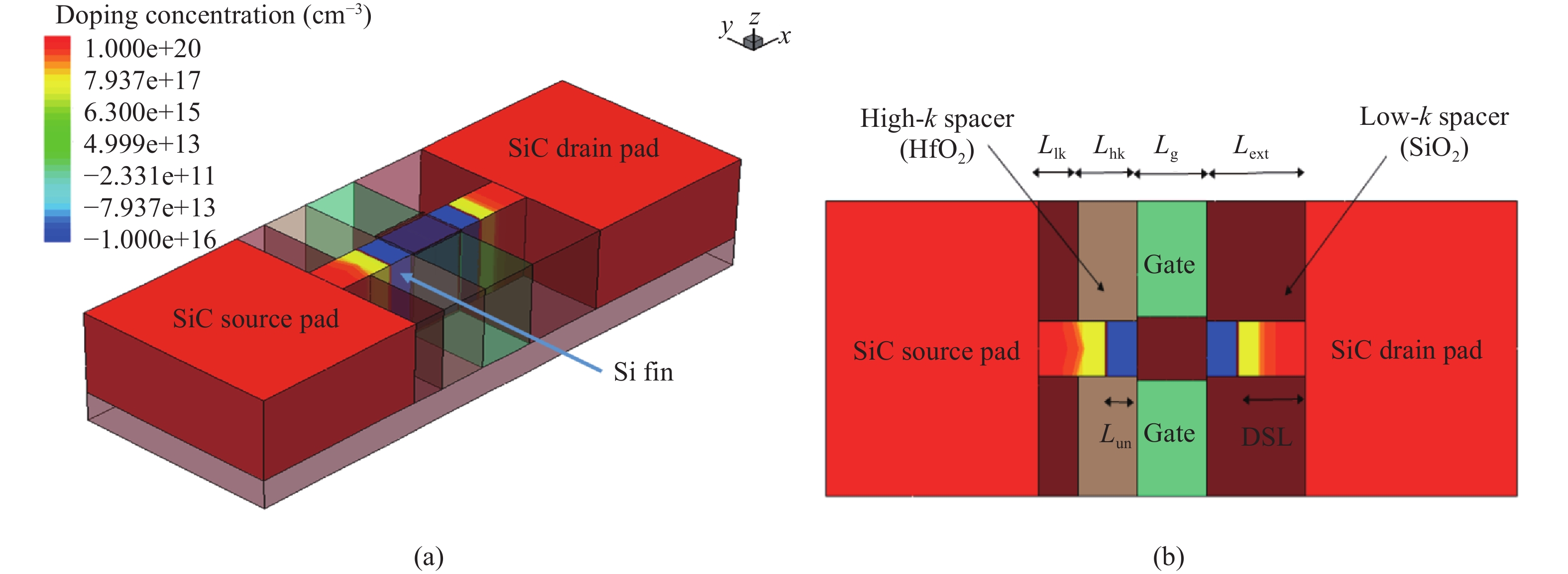
Fig. 1.
(Color online) (a) 3-D and (b) 2-D view of the proposed asymmetric dual-k SiC S/D FinFET structure in TCAD structure editor.
SEMICONDUCTOR DEVICES
Maisagalla Gopal1, , Atul Awadhiya2, Nandakishor Yadav1, S. K. Vishvakarma1 and Vaibhav Neema3
Corresponding author: Maisagalla Gopal, e-mail: phd1401102008@iiti.ac.in
Abstract: We propose a reliable asymmetric dual-k spacer with SiC source/drain (S/D) pocket as a stressor for a Si channel. This enhances the device performance in terms of electron mobility (eMobility), current driving capabilities, transconductance (Gm) and subthreshold slope (SS). The improved performance is an amalgamation of longitudinal tensile stress along the channel and reduced series resistance. We analysed the variation in drive current for different values of carbon (C) mole fraction y in Si1?yCy. It is found that the mole fraction also helps to improve device lifetime, performance enhancement also pointed by transconductance variation with the gate length. All the simulations are performed in the 3-D Sentaurus TCAD tool. The proposed device structure achieved ION = 2.17 mA/μm for Si0.3C0.7 and found that Si0.5C0.5 is more suitable for the perspective of a process variation effect for 14 nm as the gate length. We introduce reliability issues and their solutions for Si1?yCy FinFET for the first time.
Key words: asymmetric dual-k spacer, short channel effects (SCEs), SiC S/D stressors, reliability, process variation
| [1] |
Colinge J P. FinFETs and other multi-gate transistors. New York: Springer-Verlag, 2008
|
| [2] |
Hisamoto D, Lee W C, Kedzierski J, et al. FinFET—a self-aligned double-gate MOSFET scalable to 20 nm. IEEE Trans Electron Devices, 2000, 47(12): 2320 doi: 10.1109/16.887014
|
| [3] |
Frank D, Laux S, Fischetti M. Monte Carlo simulation of a 30-nm dual-gate MOSFET: how far can silicon go. IEDM Tech Dig, 1992: 553
|
| [4] |
Yadav N, Jain S, Pattanaik M, et al. A novel stability and process sensitivity driven model for optimal sized FinFET based SRAM. J Microelectron Reliab, 2015, 55(8): 1131 doi: 10.1016/j.microrel.2015.05.014
|
| [5] |
Wang Y, Cotofana S D, Fang L. Statistical reliability analysis of nbti impact on FinFET SRAMs and mitigation technique using independent-gate devices. IEEE/ACM International Symposium on Nanoscale Architectures (NANOARCH), 2012: 109
|
| [6] |
Pal P K, Kaushik B K, Anand B, et al. A comparative analysis of symmetric and asymmetric dual-k spacer FinFETs from device and circuit perspectives. 16th International Symposium Quality Electronic Design (ISQED), 2015: 594
|
| [7] |
Yang J W, Zeitzoff P M, Tseng H H. Highly manufacturable double-gate FinFET with gate-source/drain underlap. IEEE Trans Electron Devices, 2007, 54(6): 1464 doi: 10.1109/TED.2007.896387
|
| [8] |
Pradhan K P, Priyanka, Mallikarjunarao, et al. Exploration of symmetric high-k spacer (SHS) hybrid FinFET for high performance application. Superlattices Microstruct, 2015, 90: 191
|
| [9] |
Pradhan K P, Sahu P K. Benefits of asymmetric underlap dual-k spacer hybrid fin field-effect transistor over bulk fin field-effect transistor. IET Circuits Devices Syst, 2016, 10(5): 441 doi: 10.1049/iet-cds.2016.0125
|
| [10] |
Verheyen P, Collaert N, Rooyackers R, et al. 25% drive current improvement for p-type multiple gate FET (MuGFET) devices by the introduction of recessed Si0.8Ge0.2 in the source and drain regions. VLSI Tech, 2005: 194
|
| [11] |
Yang T Y, Tan K M, Lee R T P, et al. Strained n-channel FinFETs with 25 nm gate length and silicon-carbon source/drain regions for performance enhancement. VLSI Symp Tech Dig, 2006: 68
|
| [12] |
Thompson S, Armstrong M, Auth C, et al. A logic nanotechnology featuring strained-silicon. IEEE Electron Device Lett, 2004, 25(4): 191 doi: 10.1109/LED.2004.825195
|
| [13] |
Choi M, Moroz V, Smith L, et al. 14 nm FinFET stress engineering with epitaxial SiGe source/drain. IEEE Silicon-Germanium Technology and Device Meeting (ISTDM), 2012: 1
|
| [14] |
Agrawal N, Thathachary V A, Mahapatra S, et al. Impact of varying indium(x) concentration and quantum confinement on PBTI reliability in InxGa1?xAs FinFET. IEEE Electron Device Lett, 2015, 36(2): 120 doi: 10.1109/LED.2014.2385055
|
| [15] |
Cheng S Y, Chen K T, Chang S T. Impact of strain on hole mobility in the inversion layer of PMOS device with SiGe alloy thin film. Thin Solid Films, 2015, 584: 135 doi: 10.1016/j.tsf.2015.01.047
|
| [16] |
Synopsys, Inc., Sentaurus TCAD User Manual, Mountain View, 2010, CA, USA [Online]. Available: http://www.synopsys.com
|
| [17] |
Pal P K, Kaushik B K, Anand B, et al. Asymmetric dual-spacer trigate FinFET device-circuit co-design and its variability analysis. IEEE Trans Electron Devices, 2015, 62(4): 1105 doi: 10.1109/TED.2015.2400053
|
| [18] |
Anderson B A, Bryant A, Clark W F, et al. Low capacitance FET for operation at subthreshold voltages, U.S. Patent, 70092652006, 2006
|
| [19] |
Cheng K , Li X, Wise R S. Method of forming asymmetric spacers and methods of fabricating semiconductor device using asymmetric spacers. U.S. Patent, 2011/008895, 2011
|
| [20] |
The international technology roadmap for semiconductors, San Jose, CA, USA,Tech. Rep. (2013), [Online], Available: http://www.semiconductors.org/clientuploads/Research_Technology/ITRS/2013/2013Overview.pdf
|
| [21] |
Sano N, Matsuzawa K, Mukai M. On discrete random dopant modelling in drift-diffusion simulations: Physical meaning of ‘atomistic’ dopants. Micro Electron Rel, 2002, 42(2): 189
|
| [22] |
Gopal M, Sharma V, Kumar V S. Evaluation of static noise margin (SNM) of 6T SRAM cell using SiGe/SiC asymmetric dual-k spacer FinFETs. IET Micro Nano Lett, 2017, 12(12): 1028 doi: 10.1049/mnl.2017.0318
|
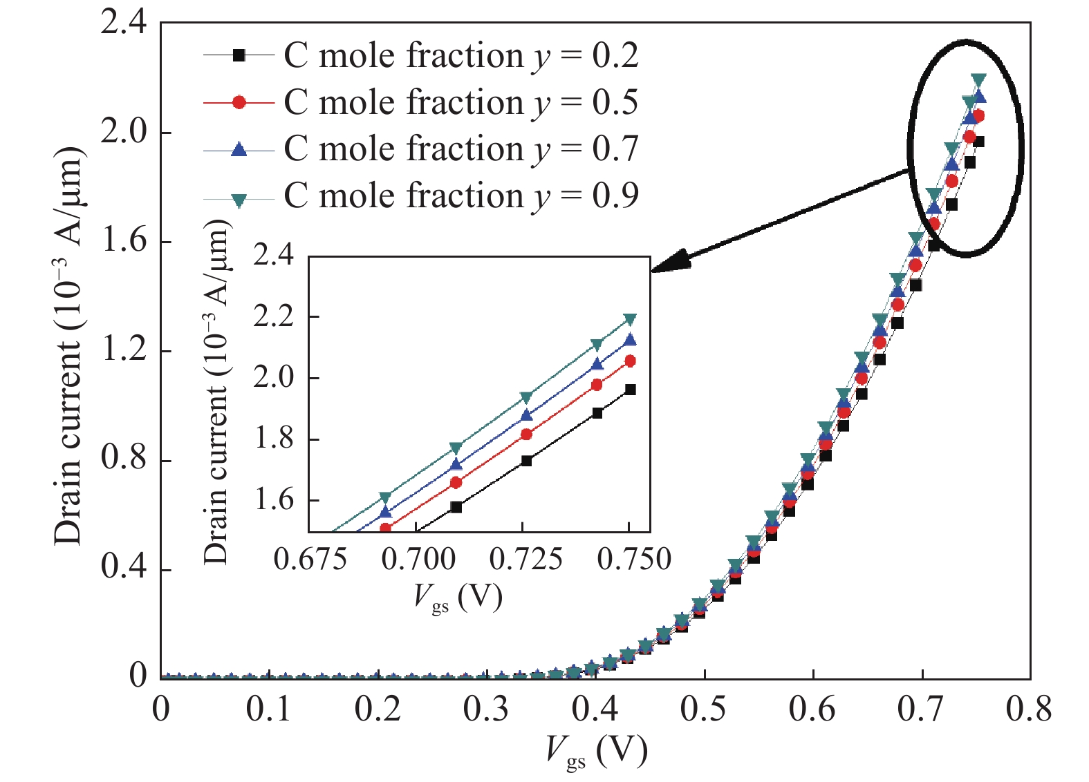
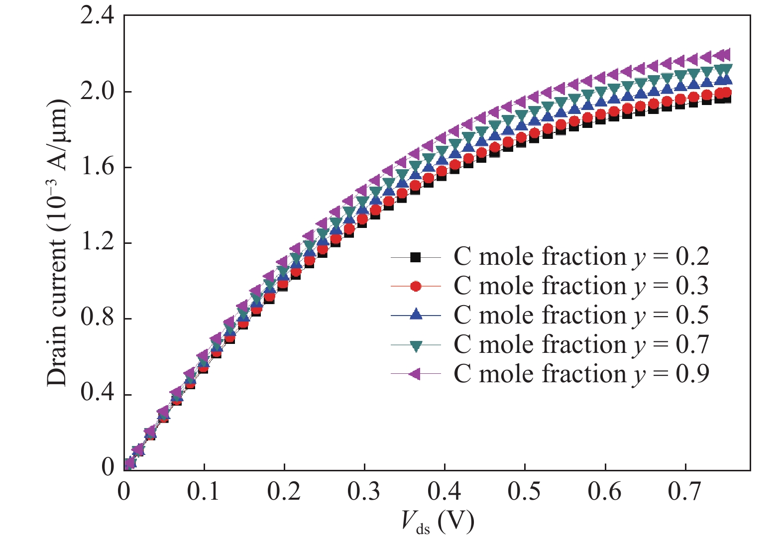
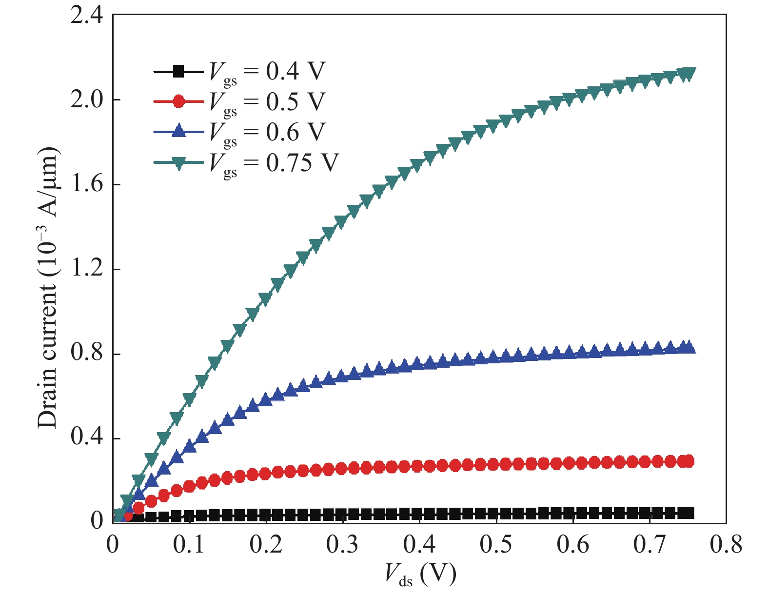
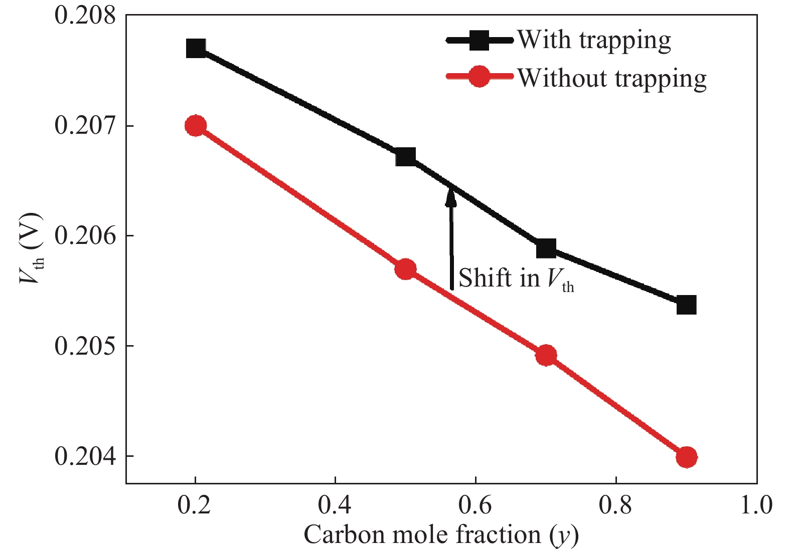
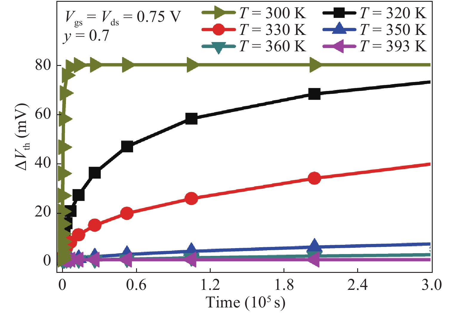
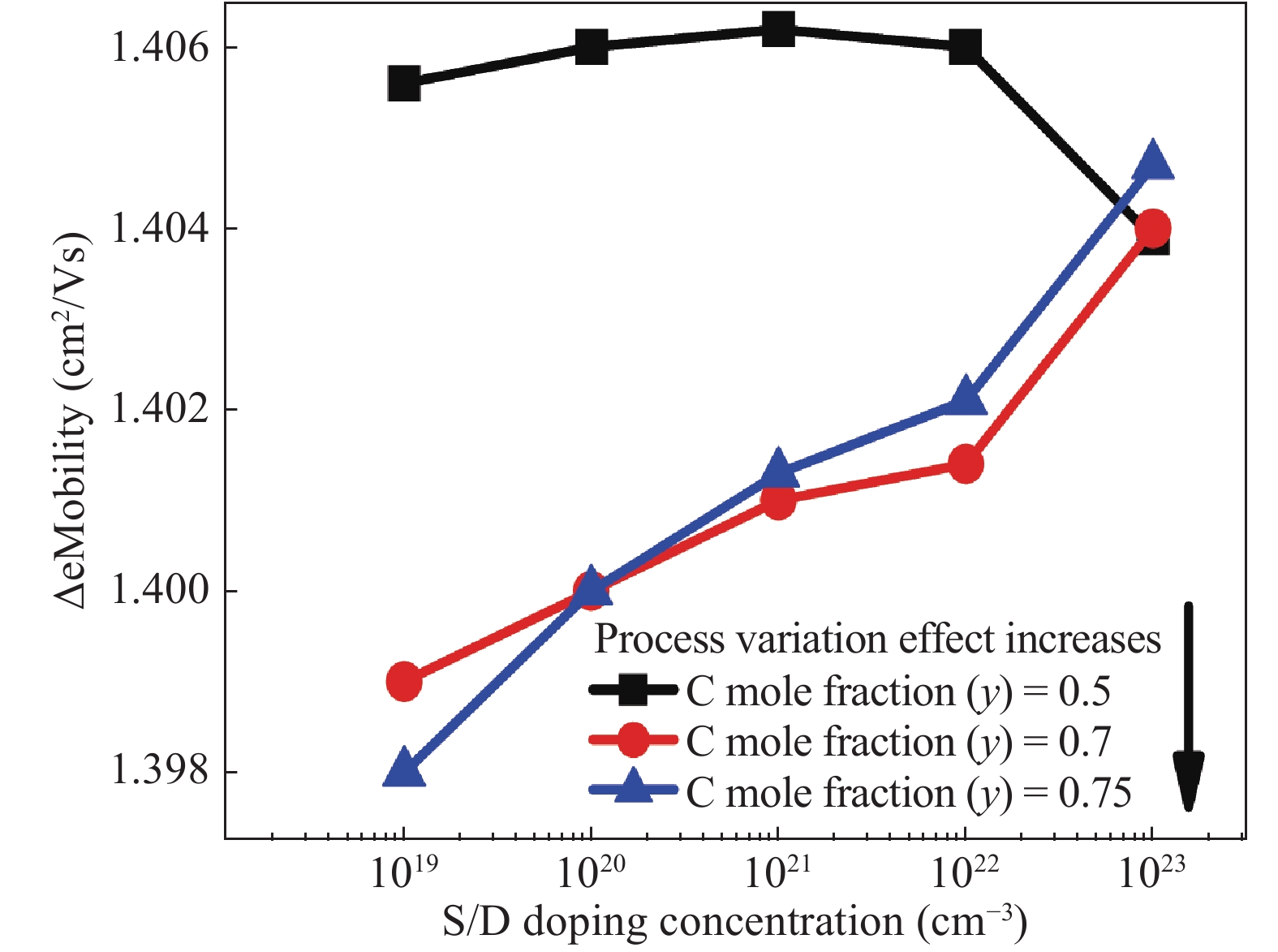
Table 1. ITRS projections for the high-performance device in the year 2017[20].
| Device parameter | ITRS projection value |
| Physical gate length (Lg) | 14 nm |
| Eq. oxide thickness (EOT) | 0.72 nm |
| Fin thickness (Tsi) | 9.4 nm |
| Supply voltage (VDD) | 0.75 V |
| Channel doping (NA) | 1 × 1016 cm?3 |
| Source/drain doping (ND) | 1 × 1020 cm?3 |
 DownLoad: CSV
| [1] |
Colinge J P. FinFETs and other multi-gate transistors. New York: Springer-Verlag, 2008
|
| [2] |
Hisamoto D, Lee W C, Kedzierski J, et al. FinFET—a self-aligned double-gate MOSFET scalable to 20 nm. IEEE Trans Electron Devices, 2000, 47(12): 2320 doi: 10.1109/16.887014
|
| [3] |
Frank D, Laux S, Fischetti M. Monte Carlo simulation of a 30-nm dual-gate MOSFET: how far can silicon go. IEDM Tech Dig, 1992: 553
|
| [4] |
Yadav N, Jain S, Pattanaik M, et al. A novel stability and process sensitivity driven model for optimal sized FinFET based SRAM. J Microelectron Reliab, 2015, 55(8): 1131 doi: 10.1016/j.microrel.2015.05.014
|
| [5] |
Wang Y, Cotofana S D, Fang L. Statistical reliability analysis of nbti impact on FinFET SRAMs and mitigation technique using independent-gate devices. IEEE/ACM International Symposium on Nanoscale Architectures (NANOARCH), 2012: 109
|
| [6] |
Pal P K, Kaushik B K, Anand B, et al. A comparative analysis of symmetric and asymmetric dual-k spacer FinFETs from device and circuit perspectives. 16th International Symposium Quality Electronic Design (ISQED), 2015: 594
|
| [7] |
Yang J W, Zeitzoff P M, Tseng H H. Highly manufacturable double-gate FinFET with gate-source/drain underlap. IEEE Trans Electron Devices, 2007, 54(6): 1464 doi: 10.1109/TED.2007.896387
|
| [8] |
Pradhan K P, Priyanka, Mallikarjunarao, et al. Exploration of symmetric high-k spacer (SHS) hybrid FinFET for high performance application. Superlattices Microstruct, 2015, 90: 191
|
| [9] |
Pradhan K P, Sahu P K. Benefits of asymmetric underlap dual-k spacer hybrid fin field-effect transistor over bulk fin field-effect transistor. IET Circuits Devices Syst, 2016, 10(5): 441 doi: 10.1049/iet-cds.2016.0125
|
| [10] |
Verheyen P, Collaert N, Rooyackers R, et al. 25% drive current improvement for p-type multiple gate FET (MuGFET) devices by the introduction of recessed Si0.8Ge0.2 in the source and drain regions. VLSI Tech, 2005: 194
|
| [11] |
Yang T Y, Tan K M, Lee R T P, et al. Strained n-channel FinFETs with 25 nm gate length and silicon-carbon source/drain regions for performance enhancement. VLSI Symp Tech Dig, 2006: 68
|
| [12] |
Thompson S, Armstrong M, Auth C, et al. A logic nanotechnology featuring strained-silicon. IEEE Electron Device Lett, 2004, 25(4): 191 doi: 10.1109/LED.2004.825195
|
| [13] |
Choi M, Moroz V, Smith L, et al. 14 nm FinFET stress engineering with epitaxial SiGe source/drain. IEEE Silicon-Germanium Technology and Device Meeting (ISTDM), 2012: 1
|
| [14] |
Agrawal N, Thathachary V A, Mahapatra S, et al. Impact of varying indium(x) concentration and quantum confinement on PBTI reliability in InxGa1?xAs FinFET. IEEE Electron Device Lett, 2015, 36(2): 120 doi: 10.1109/LED.2014.2385055
|
| [15] |
Cheng S Y, Chen K T, Chang S T. Impact of strain on hole mobility in the inversion layer of PMOS device with SiGe alloy thin film. Thin Solid Films, 2015, 584: 135 doi: 10.1016/j.tsf.2015.01.047
|
| [16] |
Synopsys, Inc., Sentaurus TCAD User Manual, Mountain View, 2010, CA, USA [Online]. Available: http://www.synopsys.com
|
| [17] |
Pal P K, Kaushik B K, Anand B, et al. Asymmetric dual-spacer trigate FinFET device-circuit co-design and its variability analysis. IEEE Trans Electron Devices, 2015, 62(4): 1105 doi: 10.1109/TED.2015.2400053
|
| [18] |
Anderson B A, Bryant A, Clark W F, et al. Low capacitance FET for operation at subthreshold voltages, U.S. Patent, 70092652006, 2006
|
| [19] |
Cheng K , Li X, Wise R S. Method of forming asymmetric spacers and methods of fabricating semiconductor device using asymmetric spacers. U.S. Patent, 2011/008895, 2011
|
| [20] |
The international technology roadmap for semiconductors, San Jose, CA, USA,Tech. Rep. (2013), [Online], Available: http://www.semiconductors.org/clientuploads/Research_Technology/ITRS/2013/2013Overview.pdf
|
| [21] |
Sano N, Matsuzawa K, Mukai M. On discrete random dopant modelling in drift-diffusion simulations: Physical meaning of ‘atomistic’ dopants. Micro Electron Rel, 2002, 42(2): 189
|
| [22] |
Gopal M, Sharma V, Kumar V S. Evaluation of static noise margin (SNM) of 6T SRAM cell using SiGe/SiC asymmetric dual-k spacer FinFETs. IET Micro Nano Lett, 2017, 12(12): 1028 doi: 10.1049/mnl.2017.0318
|


Article views: 4912 Times PDF downloads: 86 Times Cited by: 0 Times
Received: 01 February 2018 Revised: 14 March 2018 Online: Uncorrected proof: 21 May 2018Published: 09 October 2018
| Citation: |
Maisagalla Gopal, Atul Awadhiya, Nandakishor Yadav, S. K. Vishvakarma, Vaibhav Neema. Impact of varying carbon concentration in SiC S/D asymmetric dual-k spacer for high performance and reliable FinFET[J]. Journal of Semiconductors, 2018, 39(10): 104001. doi: 10.1088/1674-4926/39/10/104001
****
M Gopal, A Awadhiya, N Yadav, S K Vishvakarma, V Neema, Impact of varying carbon concentration in SiC S/D asymmetric dual-k spacer for high performance and reliable FinFET[J]. J. Semicond., 2018, 39(10): 104001. doi: 10.1088/1674-4926/39/10/104001.

|
| [1] |
Colinge J P. FinFETs and other multi-gate transistors. New York: Springer-Verlag, 2008
|
| [2] |
Hisamoto D, Lee W C, Kedzierski J, et al. FinFET—a self-aligned double-gate MOSFET scalable to 20 nm. IEEE Trans Electron Devices, 2000, 47(12): 2320 doi: 10.1109/16.887014
|
| [3] |
Frank D, Laux S, Fischetti M. Monte Carlo simulation of a 30-nm dual-gate MOSFET: how far can silicon go. IEDM Tech Dig, 1992: 553
|
| [4] |
Yadav N, Jain S, Pattanaik M, et al. A novel stability and process sensitivity driven model for optimal sized FinFET based SRAM. J Microelectron Reliab, 2015, 55(8): 1131 doi: 10.1016/j.microrel.2015.05.014
|
| [5] |
Wang Y, Cotofana S D, Fang L. Statistical reliability analysis of nbti impact on FinFET SRAMs and mitigation technique using independent-gate devices. IEEE/ACM International Symposium on Nanoscale Architectures (NANOARCH), 2012: 109
|
| [6] |
Pal P K, Kaushik B K, Anand B, et al. A comparative analysis of symmetric and asymmetric dual-k spacer FinFETs from device and circuit perspectives. 16th International Symposium Quality Electronic Design (ISQED), 2015: 594
|
| [7] |
Yang J W, Zeitzoff P M, Tseng H H. Highly manufacturable double-gate FinFET with gate-source/drain underlap. IEEE Trans Electron Devices, 2007, 54(6): 1464 doi: 10.1109/TED.2007.896387
|
| [8] |
Pradhan K P, Priyanka, Mallikarjunarao, et al. Exploration of symmetric high-k spacer (SHS) hybrid FinFET for high performance application. Superlattices Microstruct, 2015, 90: 191
|
| [9] |
Pradhan K P, Sahu P K. Benefits of asymmetric underlap dual-k spacer hybrid fin field-effect transistor over bulk fin field-effect transistor. IET Circuits Devices Syst, 2016, 10(5): 441 doi: 10.1049/iet-cds.2016.0125
|
| [10] |
Verheyen P, Collaert N, Rooyackers R, et al. 25% drive current improvement for p-type multiple gate FET (MuGFET) devices by the introduction of recessed Si0.8Ge0.2 in the source and drain regions. VLSI Tech, 2005: 194
|
| [11] |
Yang T Y, Tan K M, Lee R T P, et al. Strained n-channel FinFETs with 25 nm gate length and silicon-carbon source/drain regions for performance enhancement. VLSI Symp Tech Dig, 2006: 68
|
| [12] |
Thompson S, Armstrong M, Auth C, et al. A logic nanotechnology featuring strained-silicon. IEEE Electron Device Lett, 2004, 25(4): 191 doi: 10.1109/LED.2004.825195
|
| [13] |
Choi M, Moroz V, Smith L, et al. 14 nm FinFET stress engineering with epitaxial SiGe source/drain. IEEE Silicon-Germanium Technology and Device Meeting (ISTDM), 2012: 1
|
| [14] |
Agrawal N, Thathachary V A, Mahapatra S, et al. Impact of varying indium(x) concentration and quantum confinement on PBTI reliability in InxGa1?xAs FinFET. IEEE Electron Device Lett, 2015, 36(2): 120 doi: 10.1109/LED.2014.2385055
|
| [15] |
Cheng S Y, Chen K T, Chang S T. Impact of strain on hole mobility in the inversion layer of PMOS device with SiGe alloy thin film. Thin Solid Films, 2015, 584: 135 doi: 10.1016/j.tsf.2015.01.047
|
| [16] |
Synopsys, Inc., Sentaurus TCAD User Manual, Mountain View, 2010, CA, USA [Online]. Available: http://www.synopsys.com
|
| [17] |
Pal P K, Kaushik B K, Anand B, et al. Asymmetric dual-spacer trigate FinFET device-circuit co-design and its variability analysis. IEEE Trans Electron Devices, 2015, 62(4): 1105 doi: 10.1109/TED.2015.2400053
|
| [18] |
Anderson B A, Bryant A, Clark W F, et al. Low capacitance FET for operation at subthreshold voltages, U.S. Patent, 70092652006, 2006
|
| [19] |
Cheng K , Li X, Wise R S. Method of forming asymmetric spacers and methods of fabricating semiconductor device using asymmetric spacers. U.S. Patent, 2011/008895, 2011
|
| [20] |
The international technology roadmap for semiconductors, San Jose, CA, USA,Tech. Rep. (2013), [Online], Available: http://www.semiconductors.org/clientuploads/Research_Technology/ITRS/2013/2013Overview.pdf
|
| [21] |
Sano N, Matsuzawa K, Mukai M. On discrete random dopant modelling in drift-diffusion simulations: Physical meaning of ‘atomistic’ dopants. Micro Electron Rel, 2002, 42(2): 189
|
| [22] |
Gopal M, Sharma V, Kumar V S. Evaluation of static noise margin (SNM) of 6T SRAM cell using SiGe/SiC asymmetric dual-k spacer FinFETs. IET Micro Nano Lett, 2017, 12(12): 1028 doi: 10.1049/mnl.2017.0318
|

 WeChat ID
Journal of Semiconductors © 2017 All Rights Reserved 京ICP備05085259號-2

