


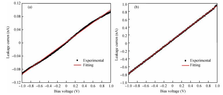
Fig. 1.
$I-V$ curves of two different Cd$_{\mathrm{0.9}}$ Zn$_{\mathrm{0.1}}$ Te:In wafers with the bias voltages from -1 to 1 V at room temperature. (a) High resistivity. (b)Low resistivity.
SEMICONDUCTOR PHYSICS
Pengfei Wang, Ruihua Nan and Zengyun Jian
Corresponding author: Pengfei Wang Email:18710748870@163.com
Abstract: The deep-level defects of CdZnTe (CZT) crystals grown by the modified vertical Bridgman (MVB) method act as trapping centers or recombination centers in the band gap, which have significant effects on its electrical properties. The resistivity and electron mobility-lifetime product of high resistivity Cd0.9Zn0.1Te wafer marked CZT1 and low resistivity Cd0.9Zn0.1Te wafer marked CZT2 were tested respectively. Their deep-level defects were identified by thermally stimulated current (TSC) spectroscopy and thermoelectric effect spectroscopy (TEES) respectively. Then the trap-related parameters were characterized by the simultaneous multiple peak analysis (SIMPA) method. The deep donor level (EDD)dominating dark current was calculated by the relationship between dark current and temperature. The Fermi-level was characterized by current-voltage measurements of temperature dependence. The width of the band gap was characterized by ultraviolet-visible-infrared transmittance spectroscopy. The results show the traps concentration and capture cross section of CZT1 are lower than CZT2, so its electron mobility-lifetime product is greater than CZT2. The Fermi-level of CZT1 is closer to the middle gap than CZT2. The degree of Fermi-level pinned by EDD of CZT1 is larger than CZT2. It can be concluded that the resistivity of CZT crystals increases as the degree of Fermi-level pinned near the middle gap by the deep donor level enlarges.
Key words: Cd0.9Zn0.1Te, deep-level defects, thermally stimulated current spectroscopy, Fermi-level, electrical properties
| [1] |
Xu L Y, Jie W Q, Zha G Q, et al. Effects of sub-bandgap illumination on electrical properties and detector performances of CdZnTe:In. Appl Phys Lett, 2014, 104:232109 doi: 10.1063/1.4883403
|
| [2] |
Gul R, Keeter K, Rodriguez R, et al. Point defects in Pb-, Bi-, and In-doped CdZnTe detectors:deep-level transient spectroscopy (DLTS) measurements. J Electron Mater, 2012, 41(3):488 doi: 10.1007/s11664-011-1802-y
|
| [3] |
Cola A, Farclla I. Electric field and current transport mechanisms in Schottky CdTe X-ray detectors under perturbing optical radiation. Sensors, 2013, 13:9414 doi: 10.3390/s130709414
|
| [4] |
Bolotnikov A, Camarda G C, Wright G W, et al. Factors limiting the performance of CdZnTe detectors. IEEE Trans Nucl Sci, 2005, 52:589 doi: 10.1109/TNS.2005.851419
|
| [5] |
Cavallini A, Fraboni B, Dusi W, et al. Behavior of CdTe and CdZnTe detectors following electron irradiation. IEEE Trans Nucl Sci, 2002, 49:1598 doi: 10.1109/TNS.2002.801683
|
| [6] |
Bolotnikov A E, Camarda G S, Cui Y, et al. Characterization and evaluation of extended defects in CZT crystals for gamma-ray detectors. J Cryst Growth, 2013, 379:46 doi: 10.1016/j.jcrysgro.2013.01.048
|
| [7] |
Zha G Q, Yang J, Xu L Y, et al. The effects of deep level traps on the electrical properties of semi-insulating CdZnTe. J Appl Phys, 2014, 115:043715 doi: 10.1063/1.4863465
|
| [8] |
Bolotnikov A E, Boggs S E, Hubertchen C M, et al. Properties of Pt Schottky type contacts on high-resistivity CdZnTe detectors. Nucl Instrum Meth A, 2002, 482(1):395 https://arxiv.org/pdf/physics/0103005
|
| [9] |
Carvalho A, Tagantsev A K, Oberg S, et al. Cation-site intrinsic defects in Zn-doped CdTe. Phys Rev B, 2010, 81(7):075215 doi: 10.1103/PhysRevB.81.075215
|
| [10] |
Nan R H, Jie W Q, Zha G Q, et al. Relationship between high resistivity and the deep level defects in CZT:In. Nucl Instrum Meth A, 2013, 705:32 doi: 10.1016/j.nima.2012.12.081
|
| [11] |
Pavlovic M, Desnica U V. Precise determination of deep trap signatures and their relative and absolute concentrations in semiinsulating GaAs. J Appl Phys, 1998, 84(4):2018 doi: 10.1063/1.368258
|
| [12] |
Nan R H, Jie W Q, Zha G Q, et al. Investigation on defect levels in CdZnTe:Al using thermally stimulated current spectroscopy. J Phys D:Appl Phys, 2010, 43:345104 doi: 10.1088/0022-3727/43/34/345104
|
| [13] |
Schlesinger T E, Toney J E, Yoon H, et al. Cadmium zinc telluride and its use as a nuclear radiation detector material. Mater Sci Eng, 2001, 32:103 doi: 10.1016/S0927-796X(01)00027-4
|
| [14] |
Nan R H, Jie W Q, Zha G Q, et al. Determination of trap levels in CZT:In by thermally stimulated current spectroscopy. Trans Nonferrous Met Soc China, 2012, 22:s148 doi: 10.1016/S1003-6326(12)61700-2
|
| [15] |
Nan R H, Jie W Q, Zha G Q, et al. Thermally stimulated current spectroscopy applied on defect characterization in semiinsulating Cd0.9Zn0.1Te. J Cryst Growth, 2012, 361:25 doi: 10.1016/j.jcrysgro.2012.09.001
|
| [16] |
Xu L Y, Jie W Q, Fu X, et al. Axial distribution of deep-level defects in as-grown CdZnTe:In ingots and their effects on the material's electrical properties. J Cryst Growth, 2015, 409:71 doi: 10.1016/j.jcrysgro.2014.09.039
|
| [17] |
Xu L Y, Jie W Q, Zhou B R, et al. Effects of crystal growth methods on deep-level defects and electrical properties of CdZnTe:In crystals. J Electron Mater, 2015, 44:518 doi: 10.1007/s11664-014-3452-3
|
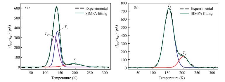
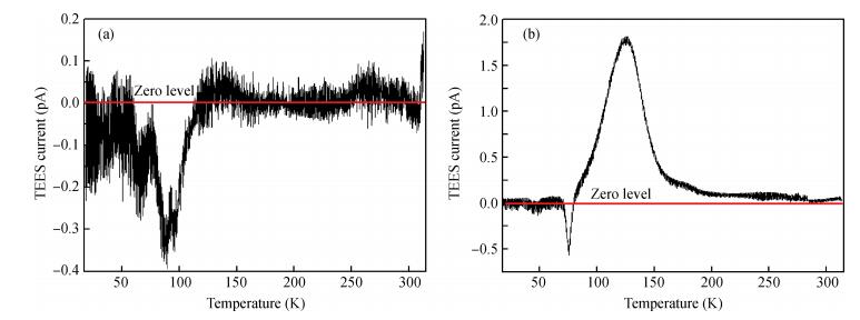
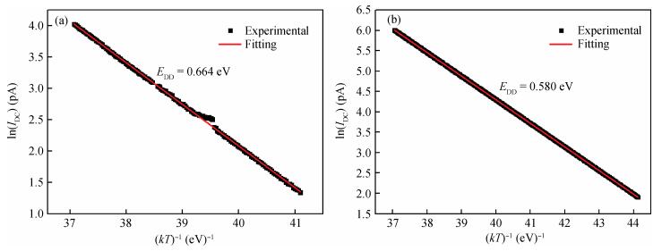
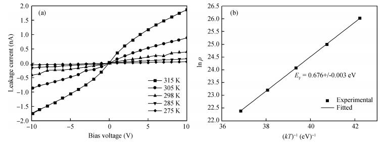
Table 1. Trap parameters of observed trap levels in CZT1 and CZT2 determined with the SIMPA method.

|


Article views: 3788 Times PDF downloads: 35 Times Cited by: 0 Times
Received: 11 November 2016 Revised: 15 December 2016 Online: Published: 01 June 2017
| Citation: |
Pengfei Wang, Ruihua Nan, Zengyun Jian. The effects of deep-level defects on the electrical properties of Cd0.9Zn0.1Te crystals[J]. Journal of Semiconductors, 2017, 38(6): 062002. doi: 10.1088/1674-4926/38/6/062002
****
P F Wang, R H Nan, Z Y Jian. The effects of deep-level defects on the electrical properties of Cd0.9Zn0.1Te crystals[J]. J. Semicond., 2017, 38(6): 062002. doi: 10.1088/1674-4926/38/6/062002.

|
Project supported by the National Natural Science Foundation of China (No. 51502234) and the Scientific Research Plan Projects of Shaanxi Provincial Department of Education of China (No. 15JS040)
the Scientific Research Plan Projects of Shaanxi Provincial Department of Education of China 15JS040
the National Natural Science Foundation of China 51502234
| [1] |
Xu L Y, Jie W Q, Zha G Q, et al. Effects of sub-bandgap illumination on electrical properties and detector performances of CdZnTe:In. Appl Phys Lett, 2014, 104:232109 doi: 10.1063/1.4883403
|
| [2] |
Gul R, Keeter K, Rodriguez R, et al. Point defects in Pb-, Bi-, and In-doped CdZnTe detectors:deep-level transient spectroscopy (DLTS) measurements. J Electron Mater, 2012, 41(3):488 doi: 10.1007/s11664-011-1802-y
|
| [3] |
Cola A, Farclla I. Electric field and current transport mechanisms in Schottky CdTe X-ray detectors under perturbing optical radiation. Sensors, 2013, 13:9414 doi: 10.3390/s130709414
|
| [4] |
Bolotnikov A, Camarda G C, Wright G W, et al. Factors limiting the performance of CdZnTe detectors. IEEE Trans Nucl Sci, 2005, 52:589 doi: 10.1109/TNS.2005.851419
|
| [5] |
Cavallini A, Fraboni B, Dusi W, et al. Behavior of CdTe and CdZnTe detectors following electron irradiation. IEEE Trans Nucl Sci, 2002, 49:1598 doi: 10.1109/TNS.2002.801683
|
| [6] |
Bolotnikov A E, Camarda G S, Cui Y, et al. Characterization and evaluation of extended defects in CZT crystals for gamma-ray detectors. J Cryst Growth, 2013, 379:46 doi: 10.1016/j.jcrysgro.2013.01.048
|
| [7] |
Zha G Q, Yang J, Xu L Y, et al. The effects of deep level traps on the electrical properties of semi-insulating CdZnTe. J Appl Phys, 2014, 115:043715 doi: 10.1063/1.4863465
|
| [8] |
Bolotnikov A E, Boggs S E, Hubertchen C M, et al. Properties of Pt Schottky type contacts on high-resistivity CdZnTe detectors. Nucl Instrum Meth A, 2002, 482(1):395 https://arxiv.org/pdf/physics/0103005
|
| [9] |
Carvalho A, Tagantsev A K, Oberg S, et al. Cation-site intrinsic defects in Zn-doped CdTe. Phys Rev B, 2010, 81(7):075215 doi: 10.1103/PhysRevB.81.075215
|
| [10] |
Nan R H, Jie W Q, Zha G Q, et al. Relationship between high resistivity and the deep level defects in CZT:In. Nucl Instrum Meth A, 2013, 705:32 doi: 10.1016/j.nima.2012.12.081
|
| [11] |
Pavlovic M, Desnica U V. Precise determination of deep trap signatures and their relative and absolute concentrations in semiinsulating GaAs. J Appl Phys, 1998, 84(4):2018 doi: 10.1063/1.368258
|
| [12] |
Nan R H, Jie W Q, Zha G Q, et al. Investigation on defect levels in CdZnTe:Al using thermally stimulated current spectroscopy. J Phys D:Appl Phys, 2010, 43:345104 doi: 10.1088/0022-3727/43/34/345104
|
| [13] |
Schlesinger T E, Toney J E, Yoon H, et al. Cadmium zinc telluride and its use as a nuclear radiation detector material. Mater Sci Eng, 2001, 32:103 doi: 10.1016/S0927-796X(01)00027-4
|
| [14] |
Nan R H, Jie W Q, Zha G Q, et al. Determination of trap levels in CZT:In by thermally stimulated current spectroscopy. Trans Nonferrous Met Soc China, 2012, 22:s148 doi: 10.1016/S1003-6326(12)61700-2
|
| [15] |
Nan R H, Jie W Q, Zha G Q, et al. Thermally stimulated current spectroscopy applied on defect characterization in semiinsulating Cd0.9Zn0.1Te. J Cryst Growth, 2012, 361:25 doi: 10.1016/j.jcrysgro.2012.09.001
|
| [16] |
Xu L Y, Jie W Q, Fu X, et al. Axial distribution of deep-level defects in as-grown CdZnTe:In ingots and their effects on the material's electrical properties. J Cryst Growth, 2015, 409:71 doi: 10.1016/j.jcrysgro.2014.09.039
|
| [17] |
Xu L Y, Jie W Q, Zhou B R, et al. Effects of crystal growth methods on deep-level defects and electrical properties of CdZnTe:In crystals. J Electron Mater, 2015, 44:518 doi: 10.1007/s11664-014-3452-3
|

 WeChat ID
Journal of Semiconductors © 2017 All Rights Reserved 京ICP備05085259號-2
 DownLoad:

