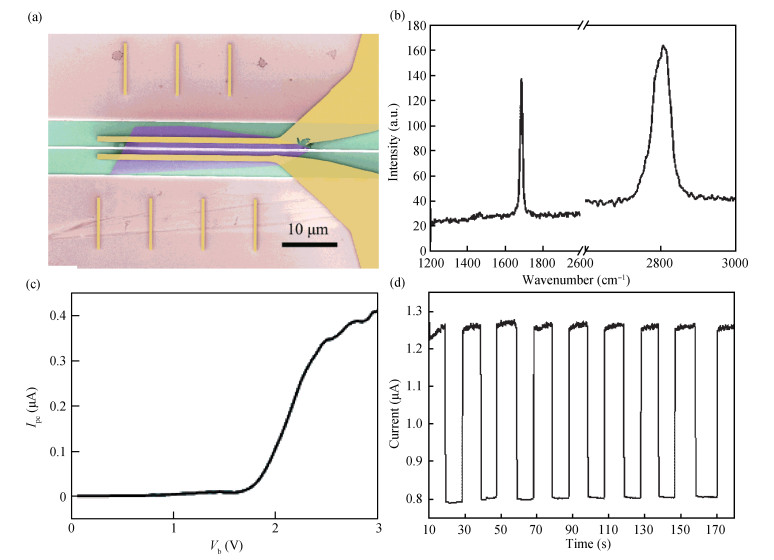
SEMICONDUCTOR TECHNOLOGY
Yubing Wang, Weihong Yin, Qin Han, Xiaohong Yang, Han Ye and Dongdong Yin
Corresponding author: Qin Han, Email: hanqin@semi.ac.cn
Abstract: Graphene field-effect transistors have been intensively studied. However, in order to fabricate devices with more complicated structures, such as the integration with waveguide and other two-dimensional materials, we need to transfer the exfoliated graphene samples to a target position. Due to the small area of exfoliated graphene and its random distribution, the transfer method requires rather high precision. In this paper, we systematically study a method to selectively transfer mechanically exfoliated graphene samples to a target position with a precision of sub-micrometer. To characterize the doping level of this method, we transfer graphene flakes to pre-patterned metal electrodes, forming graphene field-effect transistors. The hole doping of graphene is calculated to be 2.16 × 1012 cm-2. In addition, we fabricate a waveguide-integrated multilayer graphene photodetector to demonstrate the viability and accuracy of this method. A photocurrent as high as 0.4 μA is obtained, corresponding to a photoresponsivity of 0.48 mA/W. The device performs uniformly in nine illumination cycles.
Key words: graphene, field-effect transistor, flake
| [1] |
Bolotin K I, Sikes K J, Jiang Z, et al. Ultrahigh electron mobility in suspended graphene. Solid State Commun, 2008, 146(9): 351 https://www.researchgate.net/publication/222675408_Ultrahigh_electron_mobility_in_suspended_graphene
|
| [2] |
Morozov S V, Novoselov K S, Katsnelson M I, et al. Giant intrinsic carrier mobilities in graphene and its bilayer. Phys Rev Lett, 2008, 100(1): 016602 doi: 10.1103/PhysRevLett.100.016602
|
| [3] |
Nair R R, Blake P, Grigorenko A N, et al. Fine structure constant defines visual transparency of graphene. Science, 2008, 320(5881): 1308 doi: 10.1126/science.1156965
|
| [4] |
Mak K F, Sfeir M Y, Wu Y, et al. Measurement of the optical conductivity of graphene. Phys Rev Lett, 2008, 101(19): 196405 doi: 10.1103/PhysRevLett.101.196405
|
| [5] |
Lee E J H, Balasubramanian K, Weitz R T, et al. Contact and edge effects in graphene devices. Nat Nanotechnol, 2008, 3(8): 486 doi: 10.1038/nnano.2008.172
|
| [6] |
Xia F, Mueller T, Lin Y, et al. Ultrafast graphene photodetector. Nat Nanotechnol, 2009, 4(12): 839 doi: 10.1038/nnano.2009.292
|
| [7] |
Freitag M, Low T, Xia F, et al. Photoconductivity of biased graphene. Nat Photonics, 2013, 7(1): 53 http://people.ece.umn.edu/groups/tlow/Publications_files/nphoton.2012.314.pdf
|
| [8] |
Schall D, Neumaier D, Mohsin M, et al. 50 GBit/s photodetectors based on wafer-scale graphene for integrated silicon photonic communication systems. ACS Photonics, 2014, 1(9): 781 doi: 10.1021/ph5001605
|
| [9] |
Youngblood N, Anugrah Y, Ma R, et al. Multifunctional graphene optical modulator and photodetector integrated on silicon waveguides. Nano Lett, 2014, 14(5): 2741 doi: 10.1021/nl500712u
|
| [10] |
Liu M, Yin X, Ulin-Avila E, et al. A graphene-based broadband optical modulator. Nature, 2011, 474(7349): 64 doi: 10.1038/nature10067
|
| [11] |
Liu M, Yin X, Zhang X. Double-layer graphene optical modulator. Nano Lett, 2012, 12(3): 1482 doi: 10.1021/nl204202k
|
| [12] |
Gan S, Cheng C, Zhan Y, et al. A highly efficient thermo-optic microring modulator assisted by graphene. Nanoscale, 2015, 7(47): 20249 doi: 10.1039/C5NR05084G
|
| [13] |
Phare C T, Lee Y H D, Cardenas J, et al. 30 GHz Zeno-based graphene electro-optic modulator. arXiv preprint arXiv: 1411. 2053, 2014
|
| [14] |
Liu C H, Chang Y C, Norris T B, et al. Graphene photodetectors with ultra-broadband and high responsivity at room temperature. Nat Nanotechnol, 2014, 9(4): 273 doi: 10.1038/nnano.2014.31
|
| [15] |
Zhang W, Chuu C P, Huang J K, et al. Ultrahigh-gain photodetectors based on atomically thin graphene-MoS2 heterostructures. Sci Rep, 2014, 4: 32826 http://www.nature.com/articles/srep03826
|
| [16] |
Xu H, Wu J, Feng Q, et al. High responsivity and gate tunable graphene-MoS2 hybrid phototransistor. Small, 2014, 10(11): 2300 doi: 10.1002/smll.201303670
|
| [17] |
Gao L, Ni G X, Liu Y, et al. Face-to-face transfer of wafer-scale graphene films. Nature, 2014, 505(7482): 190 https://www.researchgate.net/profile/Bo_Liu32/publication/259321039_Face-to-face_transfer_of_wafer-scale_graphene_films/links/56e2395b08ae3328e076b7fb.pdf
|
| [18] |
Bae S, Kim H, Lee Y, et al. Roll-to-roll production of 30-inch graphene films for transparent electrodes. Nat Nanotechnol, 2010, 5(8): 574 doi: 10.1038/nnano.2010.132
|
| [19] |
Liang X, Sperling B A, Calizo I, et al. Toward clean and crackless transfer of graphene. ACS Nano, 2011, 5(11): 9144 doi: 10.1021/nn203377t
|
| [20] |
Moser J, Barreiro A, Bachtold A. Current-induced cleaning of graphene. Appl Phys Lett, 2007, 91(16): 163513 doi: 10.1063/1.2789673
|
| [21] |
Lin Y C, Lu C C, Yeh C H, et al. Graphene annealing: how clean can it be. Nano Lett, 2011, 12(1): 414 https://s3-eu-west-1.amazonaws.com/pstorage-acs-6854636/4206538/nl203733r_si_001.pdf
|
| [22] |
Casiraghi C, Pisana S, Novoselov K S, et al. Raman fingerprint of charged impurities in graphene. Appl Phys Lett, 2007, 91(23): 233108 doi: 10.1063/1.2818692
|
Article views: 4046 Times PDF downloads: 30 Times Cited by: 0 Times
Received: 16 June 2016 Revised: 17 November 2016 Online: Published: 01 April 2017
| Citation: |
Yubing Wang, Weihong Yin, Qin Han, Xiaohong Yang, Han Ye, Dongdong Yin. A method to transfer an individual graphene flake to a target position with a precision of sub-micrometer[J]. Journal of Semiconductors, 2017, 38(4): 046001. doi: 10.1088/1674-4926/38/4/046001
****
Y B Wang, W H Yin, Q Han, X H Yang, H Ye, D D Yin. A method to transfer an individual graphene flake to a target position with a precision of sub-micrometer[J]. J. Semicond., 2017, 38(4): 046001. doi: 10.1088/1674-4926/38/4/046001.
|
the National Natural Foundation of China 61176053
Project supported by the National Key Research and Development Program of China (No. 2016YFB0402404), the High-Tech Research and Development Program of China (Nos. 2013AA031401, 2015AA016902, 2015AA016904), and the National Natural Foundation of China (Nos. 61674136, 61176053, 61274069, 61435002)
the High-Tech Research and Development Program of China 2015AA016902
the National Key Research and Development Program of China 2016YFB0402404
the National Natural Foundation of China 61435002
the High-Tech Research and Development Program of China 2013AA031401
the High-Tech Research and Development Program of China 2015AA016904
the National Natural Foundation of China 61274069
the National Natural Foundation of China 61674136
| [1] |
Bolotin K I, Sikes K J, Jiang Z, et al. Ultrahigh electron mobility in suspended graphene. Solid State Commun, 2008, 146(9): 351 https://www.researchgate.net/publication/222675408_Ultrahigh_electron_mobility_in_suspended_graphene
|
| [2] |
Morozov S V, Novoselov K S, Katsnelson M I, et al. Giant intrinsic carrier mobilities in graphene and its bilayer. Phys Rev Lett, 2008, 100(1): 016602 doi: 10.1103/PhysRevLett.100.016602
|
| [3] |
Nair R R, Blake P, Grigorenko A N, et al. Fine structure constant defines visual transparency of graphene. Science, 2008, 320(5881): 1308 doi: 10.1126/science.1156965
|
| [4] |
Mak K F, Sfeir M Y, Wu Y, et al. Measurement of the optical conductivity of graphene. Phys Rev Lett, 2008, 101(19): 196405 doi: 10.1103/PhysRevLett.101.196405
|
| [5] |
Lee E J H, Balasubramanian K, Weitz R T, et al. Contact and edge effects in graphene devices. Nat Nanotechnol, 2008, 3(8): 486 doi: 10.1038/nnano.2008.172
|
| [6] |
Xia F, Mueller T, Lin Y, et al. Ultrafast graphene photodetector. Nat Nanotechnol, 2009, 4(12): 839 doi: 10.1038/nnano.2009.292
|
| [7] |
Freitag M, Low T, Xia F, et al. Photoconductivity of biased graphene. Nat Photonics, 2013, 7(1): 53 http://people.ece.umn.edu/groups/tlow/Publications_files/nphoton.2012.314.pdf
|
| [8] |
Schall D, Neumaier D, Mohsin M, et al. 50 GBit/s photodetectors based on wafer-scale graphene for integrated silicon photonic communication systems. ACS Photonics, 2014, 1(9): 781 doi: 10.1021/ph5001605
|
| [9] |
Youngblood N, Anugrah Y, Ma R, et al. Multifunctional graphene optical modulator and photodetector integrated on silicon waveguides. Nano Lett, 2014, 14(5): 2741 doi: 10.1021/nl500712u
|
| [10] |
Liu M, Yin X, Ulin-Avila E, et al. A graphene-based broadband optical modulator. Nature, 2011, 474(7349): 64 doi: 10.1038/nature10067
|
| [11] |
Liu M, Yin X, Zhang X. Double-layer graphene optical modulator. Nano Lett, 2012, 12(3): 1482 doi: 10.1021/nl204202k
|
| [12] |
Gan S, Cheng C, Zhan Y, et al. A highly efficient thermo-optic microring modulator assisted by graphene. Nanoscale, 2015, 7(47): 20249 doi: 10.1039/C5NR05084G
|
| [13] |
Phare C T, Lee Y H D, Cardenas J, et al. 30 GHz Zeno-based graphene electro-optic modulator. arXiv preprint arXiv: 1411. 2053, 2014
|
| [14] |
Liu C H, Chang Y C, Norris T B, et al. Graphene photodetectors with ultra-broadband and high responsivity at room temperature. Nat Nanotechnol, 2014, 9(4): 273 doi: 10.1038/nnano.2014.31
|
| [15] |
Zhang W, Chuu C P, Huang J K, et al. Ultrahigh-gain photodetectors based on atomically thin graphene-MoS2 heterostructures. Sci Rep, 2014, 4: 32826 http://www.nature.com/articles/srep03826
|
| [16] |
Xu H, Wu J, Feng Q, et al. High responsivity and gate tunable graphene-MoS2 hybrid phototransistor. Small, 2014, 10(11): 2300 doi: 10.1002/smll.201303670
|
| [17] |
Gao L, Ni G X, Liu Y, et al. Face-to-face transfer of wafer-scale graphene films. Nature, 2014, 505(7482): 190 https://www.researchgate.net/profile/Bo_Liu32/publication/259321039_Face-to-face_transfer_of_wafer-scale_graphene_films/links/56e2395b08ae3328e076b7fb.pdf
|
| [18] |
Bae S, Kim H, Lee Y, et al. Roll-to-roll production of 30-inch graphene films for transparent electrodes. Nat Nanotechnol, 2010, 5(8): 574 doi: 10.1038/nnano.2010.132
|
| [19] |
Liang X, Sperling B A, Calizo I, et al. Toward clean and crackless transfer of graphene. ACS Nano, 2011, 5(11): 9144 doi: 10.1021/nn203377t
|
| [20] |
Moser J, Barreiro A, Bachtold A. Current-induced cleaning of graphene. Appl Phys Lett, 2007, 91(16): 163513 doi: 10.1063/1.2789673
|
| [21] |
Lin Y C, Lu C C, Yeh C H, et al. Graphene annealing: how clean can it be. Nano Lett, 2011, 12(1): 414 https://s3-eu-west-1.amazonaws.com/pstorage-acs-6854636/4206538/nl203733r_si_001.pdf
|
| [22] |
Casiraghi C, Pisana S, Novoselov K S, et al. Raman fingerprint of charged impurities in graphene. Appl Phys Lett, 2007, 91(23): 233108 doi: 10.1063/1.2818692
|
Journal of Semiconductors © 2017 All Rights Reserved 京ICP備05085259號(hào)-2