


Fig. 1.
(Color online) Schematic diagram of a semi-closed diffusion device and the placement of the Zn3P2 particles and InP wafer.
SEMICONDUCTOR DEVICES
Guifeng Chen1, Mengxue Wang1, 2, Wenxian Yang2, Ming Tan2, Yuanyuan Wu2, Pan Dai2, Yuyang Huang3 and Shulong Lu2,
Corresponding author: Shulong Lu, Email: sllu2008@sinano.ac.cn
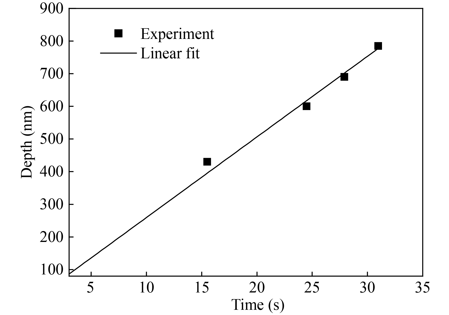
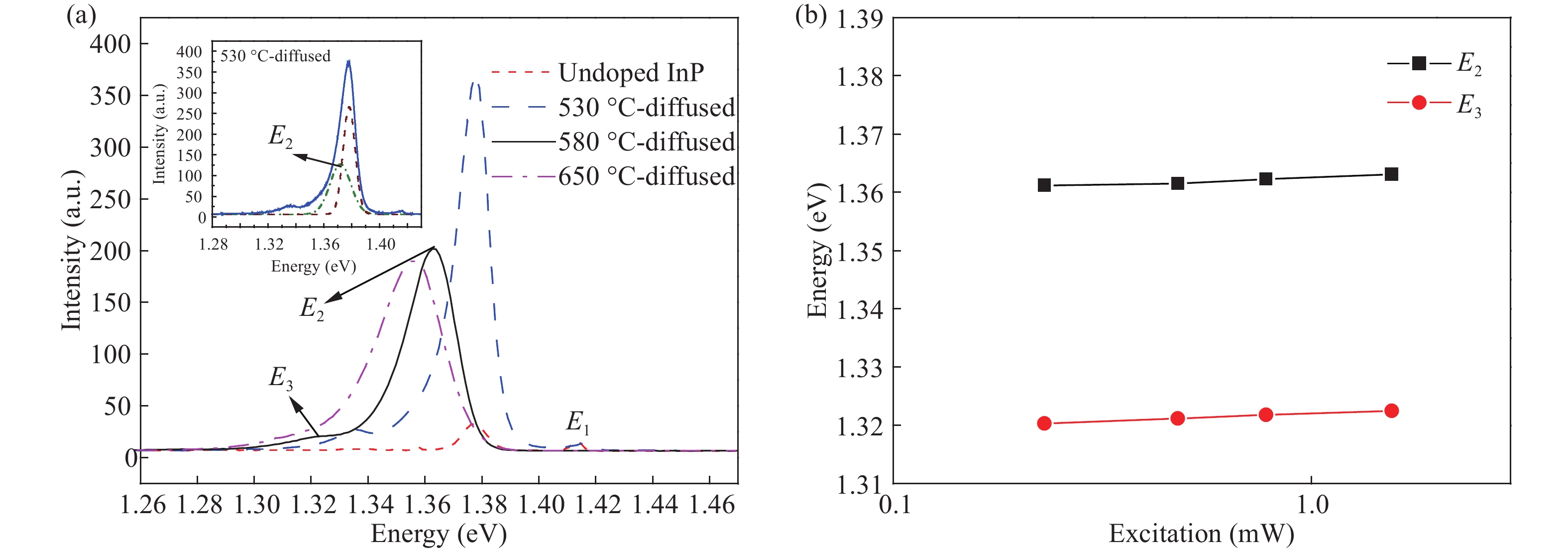
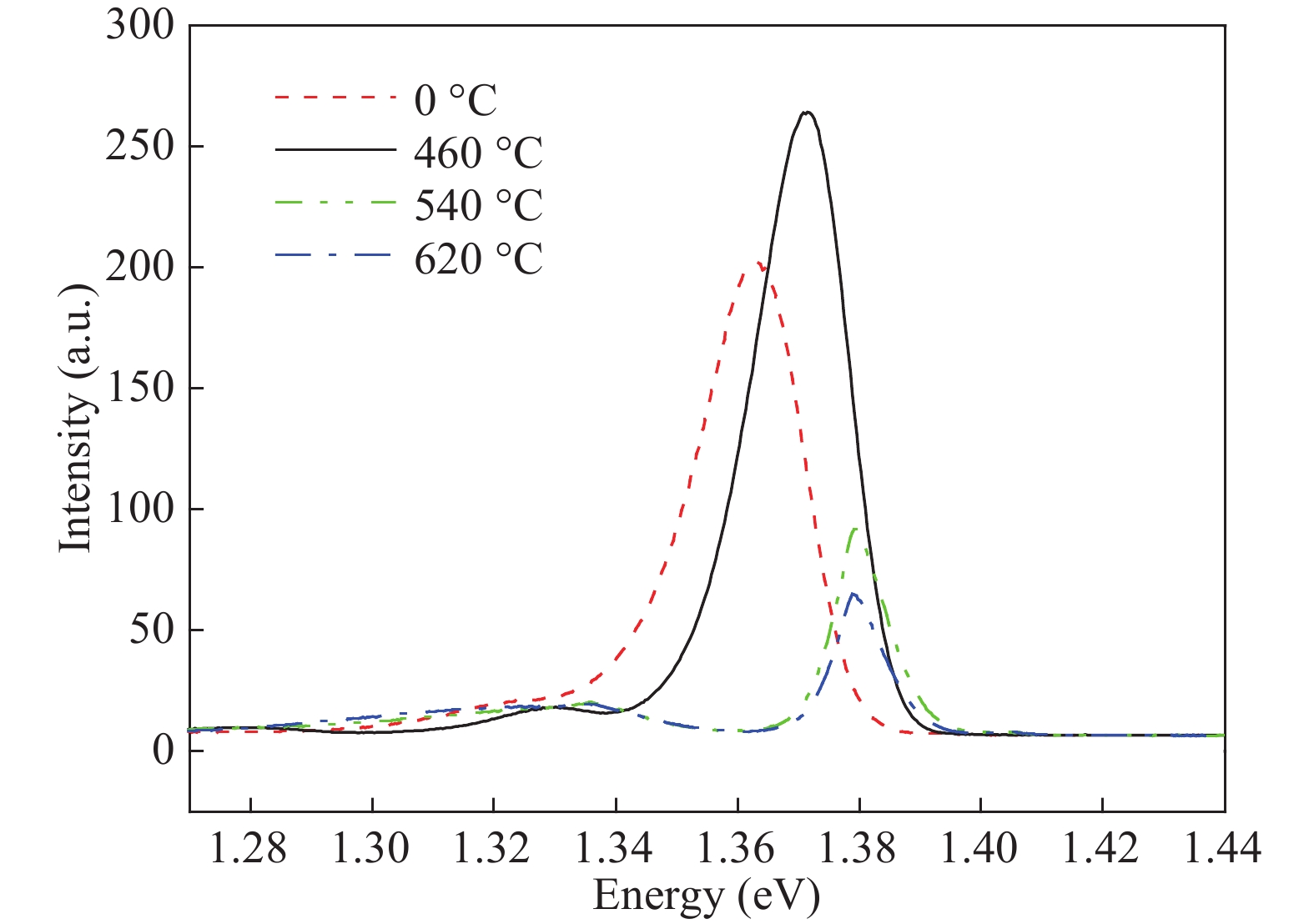
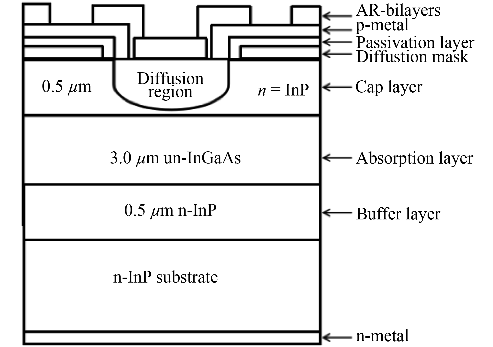
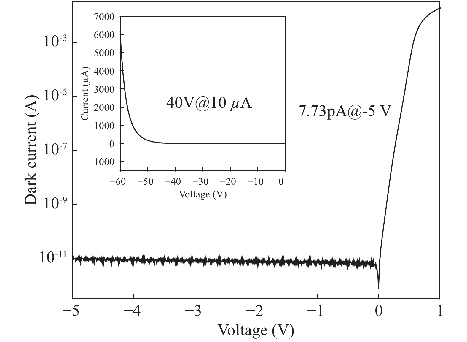
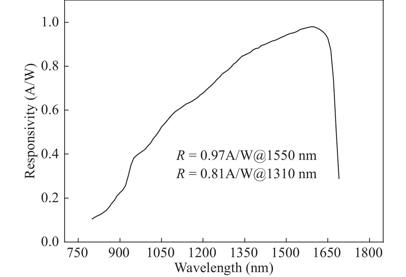
Abstract: Zn diffusion into InP was carried out ex-situ using a new Zn diffusion technique with zinc phosphorus particles placed around InP materials as zinc source in a semi-closed chamber formed by a modified diffusion furnace. The optical characteristics of the Zn-diffused InP layer for the planar-type InGaAs/InP PIN photodetectors grown by molecular beam epitaxy (MBE) has been investigated by photoluminescence (PL) measurements. The temperature-dependent PL spectrum of Zn-diffused InP samples at different diffusion temperatures showed that band-to-acceptor transition dominates the PL emission, which indicates that Zn was commendably diffused into InP layer as the acceptor. High quality Zn-diffused InP layer with typically smooth surface was obtained at 580 °C for 10 min. Furthermore, more interstitial Zn atoms were activated to act as acceptors after a rapid annealing process. Based on the above Zn-diffusion technique, a 50 μm planar-type InGaAs/InP PIN photodector device was fabricated and exhibited a low dark current of 7.73 pA under a reverse bias potential of ?5 V and a high breakdown voltage of larger than 41 V (I < 10 μA). In addition, a high responsivity of 0.81 A/W at 1.31 μm and 0.97 A/W at 1.55 μm was obtained in the developed PIN photodetector.
Key words: Zn diffusion, semi-closed, InGaAs/InP PIN photodetectors, photoluminescence (PL), dark current, responsivity
| [1] |
Jin L F, Zhang Y T, Wang H Y, et al. Accelerated aging of InGaAs PIN photoelectric detectors. Chin J Lasers, 2014, 41(10): 1008002 doi: 10.3788/CJL
|
| [2] |
Yue Z G. Xenics InGaAs SWIR detector is part of Proba-V space mission. Infrares, 2013, 34(7): 19
|
| [3] |
Liu S Q, Han Q, Yang X H, et al. Fabrication and characterization of high-speed and high-efficience photodetector. Laser Optoelectron Prog, 2012, 49(2): 138
|
| [4] |
Dave H, Dewan C, Paul S, et al. AWiFS camera for Resourcesat. Asia-Pacific Remote Sensing Symposium. International Society for Optics and Photonics, 2006: 23
|
| [5] |
Macdougal M H, Geske J C, Wang C, et al. Short-wavelength infrared imaging using low dark current InGaAs detector arrays and vertical-cavity surface-emitting laser illuminators. Mathematics Teacher, 2011, 50(6):1011
|
| [6] |
Wang Y S, Chang S J, Tsai C L, et al. 10-Gb/s planar InGaAs P-I-N photodetectors. IEEE Sens J, 2010, 10(10): 1559 doi: 10.1109/JSEN.2010.2046888
|
| [7] |
Pereira J T, Torres J. Frequency response optimization of dual depletion InGaAs/InP PIN photodiodes. Photonic Sens, 2016, 6(1): 63 doi: 10.1007/s13320-015-0296-2
|
| [8] |
Wang G, Yoneda Y, Aono H, et al. Highly reliable high performance waveguide-integrated InP/InGaAs pin photodiodes for 40 Gbit/s fibre-optical communication application. Electron Lett, 2003, 39(15): 1147 doi: 10.1049/el:20030725
|
| [9] |
Lee Y L, Huang C C, Ho C L, et al. Planar InGaAs p-i-n Photodiodes With Transparent-Conducting-Based Antireflection and Double-Path Reflector. IEEE Electron Device Letters, 2013, 34(11): 1406 doi: 10.1109/LED.2013.2281830
|
| [10] |
Skrimshire C P, Farr J R, Sloan D F, et al. Reliability of mesa and planar InGaAs PIN photodiodes. IEE Proce J Optoelectron, 1990, 137(1): 74 doi: 10.1049/ip-j.1990.0015
|
| [11] |
Ravi M R, Dasgupta A, Dasgupta N. Silicon nitride and polyimide capping layers on InGaAs/InP PIN photodetector after sulfur treatment. J Cryst Growth, 2004, 268(3-4): 359 doi: 10.1016/j.jcrysgro.2004.04.054
|
| [12] |
Chan L Y, Yu K M, Ben-Tzur M, et al. Lattice location of diffused Zn atoms in GaAs and InP single crystals. J Appl Phys, 1991, 69(5): 2998 doi: 10.1063/1.348613
|
| [13] |
Islam M, Feng J Y, Berkovich A, et al. InGaAs/InP PIN photodetector arrays made by MOCVD based zinc diffusion processes. SPIE Defense+Security. 2016: 98190G
|
| [14] |
Ettenberg M H, Lange M J, Sugg A R, et al. Zinc diffusion in InAsP/InGaAs heterostructures. J Electron Mater, 1999, 28(12): 1433 doi: 10.1007/s11664-999-0136-5
|
| [15] |
Wada M, Izumi K, Sakakibara K. Diffusion of zinc acceptors in InAsP by the metal–organic vapor-phase diffusion technique. Appl Phys Lett, 1997, 71(7): 900 doi: 10.1063/1.119682
|
| [16] |
Pitts O J, Hisko M, Benyon W, et al. MOCVD based zinc diffusion process for planar InP/InGaAs avalanche photodiode fabrication. International Conference on Indium Phosphide and Related Materials. 2012: 225
|
| [17] |
Howard A J, Pathangey B, Hayakawa Y, et al. Application of the point-defect analysis technique to zinc doping of MOCVD indium phosphide. Semicond Sci Technol, 2003, 18(8): 723 doi: 10.1088/0268-1242/18/8/301
|
| [18] |
Tang H, Wu X, Zhang K, et al. High uniformity InGaAs linear mesa-type SWIR focal plane arrays. Infrared Mater Devices Appl, 2008, 6835: 683516
|
| [19] |
Kurishima K, Kobayashi T, Ito H, et al. Control of Zn diffusion in InP/InGaAs heterojunction bipolar transistor structures grown by metalorganic vapor phase epitaxy. J Appl Phys, 1996, 79(8): 4017 doi: 10.1063/1.361830
|
| [20] |
Huang C C, Ho C L, Lee Y L, et al. Large-area planar InGaAs p-i-n photodiodes with Mg driven-in by rapid thermal diffusion. IEEE Electron Device Letters, 2014, 35(12): 1278 doi: 10.1109/LED.2014.2362687
|
| [21] |
Huang C C, Ho C L, Wu M C. Large-area planar wavelength-extended InGaAs p–i–n photodiodes by using rapid thermal diffusion with spin-on dopant technique. IEEE Electron Device Lett, 2015, 36(8): 820 doi: 10.1109/LED.2015.2445471
|
| [22] |
Erman M, Gillardin G, Bris J L, et al. Characterization of Fe-doped semi-insulating InP by low temperature and room temperature spatially resolved photoluminescence. J Cryst Growth, 1989, 96(3): 469 doi: 10.1016/0022-0248(89)90041-9
|
| [23] |
Moon Y, Si S, Yoon E, et al. Low temperature photoluminescence characteristics of Zn-doped InP grown by metalorganic chemical vapor deposition. J Appl Phys, 1998, 83(4): 2261 doi: 10.1063/1.366966
|
| [24] |
Dingle R. Luminescent transitions associated with divalent copper impurities and the green emission from semiconducting zinc oxide. Phys Rev Lett, 1969, 23(11): 579 doi: 10.1103/PhysRevLett.23.579
|
| [25] |
Kim T S, Lester S D, Streetman B G. Studies of the 1.35-eV photoluminescence band in InP. J Appl Phys, 1987, 62(4): 1363 doi: 10.1063/1.339639
|
| [26] |
Temkin H, Dutt B V, Bonner W A. Photoluminescence study of native defects in InP. Appl Phys Lett, 1981, 38(6): 431 doi: 10.1063/1.92386
|
| [27] |
Hsu J K, Juang C, Lee B J, et al. Photoluminescence studies of interstitial Zn in InP due to rapid thermal annealing. J Vac Sci Technol B, 1994, 12(3): 1416 doi: 10.1116/1.587310
|
| [28] |
Montie E A, Gurp G J V. Photoluminescence of Zn-diffused and annealed InP. J Appl Phys, 1989, 66(11): 5549 doi: 10.1063/1.343659
|
| [29] |
Wong C D, Bube R H. Bulk and surface effects of heat treatment of p-type InP crystals. J Appl Phys, 1984, 55(10): 3804 doi: 10.1063/1.332889
|
| [30] |
Hess K, Stath N, Benz K W. Liquid phase epitaxy of InP. J Electrocheml Soc, 1974, 121(9): 1208 doi: 10.1149/1.2402014
|
| [31] |
Kubota E, Ohmori Y, Sugii K. Electrical and optical properties of Mg–, Ca–, and Zn– doped InP crystals grown by the synthesis, solute diffusion technique. J Appl Phys, 1984, 55(10): 3779 doi: 10.1063/1.332934
|
| [32] |
Yoon K H, Lee Y H, Yeo D H, et al. The characteristics of Zn-doped InP using spin-on dopant as a diffusion source. Journal of Electronic Materials, 2002, 31(4): 244 doi: 10.1007/s11664-002-0139-y
|
| [33] |
Borghesi A, Guizzetti G, Patrini M, et al. Infrared study and characterization of Zn diffused InP. J Appl Phys, 1993, 74(4): 2445 doi: 10.1063/1.354681
|
| [34] |
Ishikawa T, Inata T, Kondo K, et al. Annealing effect in Si-doped GaAs and AlGaAs layers grown by MBE. Electron Lett, 1986, 22(4): 189 doi: 10.1049/el:19860132
|


Article views: 6139 Times PDF downloads: 300 Times Cited by: 0 Times
Received: 10 April 2017 Revised: 19 May 2017 Online: Uncorrected proof: 11 November 2017Corrected proof: 15 November 2017Published: 01 December 2017
| Citation: |
Guifeng Chen, Mengxue Wang, Wenxian Yang, Ming Tan, Yuanyuan Wu, Pan Dai, Yuyang Huang, Shulong Lu. Optical properties of Zn-diffused InP layers for the planar-type InGaAs/InP photodetectors[J]. Journal of Semiconductors, 2017, 38(12): 124004. doi: 10.1088/1674-4926/38/12/124004
****
G F Chen, M X Wang, W X Yang, M Tan, Y Y Wu, P Dai, Y Y Huang, S L Lu. Optical properties of Zn-diffused InP layers for the planar-type InGaAs/InP photodetectors[J]. J. Semicond., 2017, 38(12): 124004. doi: 10.1088/1674-4926/38/12/124004.

|
Project supported by the Key R&D Program of Jiangsu Province (No. BE2016085) , the National Natural Science Foundation of China (Nos. 61674051), and the External Cooperation Program of BIC, Chinese Academy of Sciences (No. 121E32KYSB20160071).
| [1] |
Jin L F, Zhang Y T, Wang H Y, et al. Accelerated aging of InGaAs PIN photoelectric detectors. Chin J Lasers, 2014, 41(10): 1008002 doi: 10.3788/CJL
|
| [2] |
Yue Z G. Xenics InGaAs SWIR detector is part of Proba-V space mission. Infrares, 2013, 34(7): 19
|
| [3] |
Liu S Q, Han Q, Yang X H, et al. Fabrication and characterization of high-speed and high-efficience photodetector. Laser Optoelectron Prog, 2012, 49(2): 138
|
| [4] |
Dave H, Dewan C, Paul S, et al. AWiFS camera for Resourcesat. Asia-Pacific Remote Sensing Symposium. International Society for Optics and Photonics, 2006: 23
|
| [5] |
Macdougal M H, Geske J C, Wang C, et al. Short-wavelength infrared imaging using low dark current InGaAs detector arrays and vertical-cavity surface-emitting laser illuminators. Mathematics Teacher, 2011, 50(6):1011
|
| [6] |
Wang Y S, Chang S J, Tsai C L, et al. 10-Gb/s planar InGaAs P-I-N photodetectors. IEEE Sens J, 2010, 10(10): 1559 doi: 10.1109/JSEN.2010.2046888
|
| [7] |
Pereira J T, Torres J. Frequency response optimization of dual depletion InGaAs/InP PIN photodiodes. Photonic Sens, 2016, 6(1): 63 doi: 10.1007/s13320-015-0296-2
|
| [8] |
Wang G, Yoneda Y, Aono H, et al. Highly reliable high performance waveguide-integrated InP/InGaAs pin photodiodes for 40 Gbit/s fibre-optical communication application. Electron Lett, 2003, 39(15): 1147 doi: 10.1049/el:20030725
|
| [9] |
Lee Y L, Huang C C, Ho C L, et al. Planar InGaAs p-i-n Photodiodes With Transparent-Conducting-Based Antireflection and Double-Path Reflector. IEEE Electron Device Letters, 2013, 34(11): 1406 doi: 10.1109/LED.2013.2281830
|
| [10] |
Skrimshire C P, Farr J R, Sloan D F, et al. Reliability of mesa and planar InGaAs PIN photodiodes. IEE Proce J Optoelectron, 1990, 137(1): 74 doi: 10.1049/ip-j.1990.0015
|
| [11] |
Ravi M R, Dasgupta A, Dasgupta N. Silicon nitride and polyimide capping layers on InGaAs/InP PIN photodetector after sulfur treatment. J Cryst Growth, 2004, 268(3-4): 359 doi: 10.1016/j.jcrysgro.2004.04.054
|
| [12] |
Chan L Y, Yu K M, Ben-Tzur M, et al. Lattice location of diffused Zn atoms in GaAs and InP single crystals. J Appl Phys, 1991, 69(5): 2998 doi: 10.1063/1.348613
|
| [13] |
Islam M, Feng J Y, Berkovich A, et al. InGaAs/InP PIN photodetector arrays made by MOCVD based zinc diffusion processes. SPIE Defense+Security. 2016: 98190G
|
| [14] |
Ettenberg M H, Lange M J, Sugg A R, et al. Zinc diffusion in InAsP/InGaAs heterostructures. J Electron Mater, 1999, 28(12): 1433 doi: 10.1007/s11664-999-0136-5
|
| [15] |
Wada M, Izumi K, Sakakibara K. Diffusion of zinc acceptors in InAsP by the metal–organic vapor-phase diffusion technique. Appl Phys Lett, 1997, 71(7): 900 doi: 10.1063/1.119682
|
| [16] |
Pitts O J, Hisko M, Benyon W, et al. MOCVD based zinc diffusion process for planar InP/InGaAs avalanche photodiode fabrication. International Conference on Indium Phosphide and Related Materials. 2012: 225
|
| [17] |
Howard A J, Pathangey B, Hayakawa Y, et al. Application of the point-defect analysis technique to zinc doping of MOCVD indium phosphide. Semicond Sci Technol, 2003, 18(8): 723 doi: 10.1088/0268-1242/18/8/301
|
| [18] |
Tang H, Wu X, Zhang K, et al. High uniformity InGaAs linear mesa-type SWIR focal plane arrays. Infrared Mater Devices Appl, 2008, 6835: 683516
|
| [19] |
Kurishima K, Kobayashi T, Ito H, et al. Control of Zn diffusion in InP/InGaAs heterojunction bipolar transistor structures grown by metalorganic vapor phase epitaxy. J Appl Phys, 1996, 79(8): 4017 doi: 10.1063/1.361830
|
| [20] |
Huang C C, Ho C L, Lee Y L, et al. Large-area planar InGaAs p-i-n photodiodes with Mg driven-in by rapid thermal diffusion. IEEE Electron Device Letters, 2014, 35(12): 1278 doi: 10.1109/LED.2014.2362687
|
| [21] |
Huang C C, Ho C L, Wu M C. Large-area planar wavelength-extended InGaAs p–i–n photodiodes by using rapid thermal diffusion with spin-on dopant technique. IEEE Electron Device Lett, 2015, 36(8): 820 doi: 10.1109/LED.2015.2445471
|
| [22] |
Erman M, Gillardin G, Bris J L, et al. Characterization of Fe-doped semi-insulating InP by low temperature and room temperature spatially resolved photoluminescence. J Cryst Growth, 1989, 96(3): 469 doi: 10.1016/0022-0248(89)90041-9
|
| [23] |
Moon Y, Si S, Yoon E, et al. Low temperature photoluminescence characteristics of Zn-doped InP grown by metalorganic chemical vapor deposition. J Appl Phys, 1998, 83(4): 2261 doi: 10.1063/1.366966
|
| [24] |
Dingle R. Luminescent transitions associated with divalent copper impurities and the green emission from semiconducting zinc oxide. Phys Rev Lett, 1969, 23(11): 579 doi: 10.1103/PhysRevLett.23.579
|
| [25] |
Kim T S, Lester S D, Streetman B G. Studies of the 1.35-eV photoluminescence band in InP. J Appl Phys, 1987, 62(4): 1363 doi: 10.1063/1.339639
|
| [26] |
Temkin H, Dutt B V, Bonner W A. Photoluminescence study of native defects in InP. Appl Phys Lett, 1981, 38(6): 431 doi: 10.1063/1.92386
|
| [27] |
Hsu J K, Juang C, Lee B J, et al. Photoluminescence studies of interstitial Zn in InP due to rapid thermal annealing. J Vac Sci Technol B, 1994, 12(3): 1416 doi: 10.1116/1.587310
|
| [28] |
Montie E A, Gurp G J V. Photoluminescence of Zn-diffused and annealed InP. J Appl Phys, 1989, 66(11): 5549 doi: 10.1063/1.343659
|
| [29] |
Wong C D, Bube R H. Bulk and surface effects of heat treatment of p-type InP crystals. J Appl Phys, 1984, 55(10): 3804 doi: 10.1063/1.332889
|
| [30] |
Hess K, Stath N, Benz K W. Liquid phase epitaxy of InP. J Electrocheml Soc, 1974, 121(9): 1208 doi: 10.1149/1.2402014
|
| [31] |
Kubota E, Ohmori Y, Sugii K. Electrical and optical properties of Mg–, Ca–, and Zn– doped InP crystals grown by the synthesis, solute diffusion technique. J Appl Phys, 1984, 55(10): 3779 doi: 10.1063/1.332934
|
| [32] |
Yoon K H, Lee Y H, Yeo D H, et al. The characteristics of Zn-doped InP using spin-on dopant as a diffusion source. Journal of Electronic Materials, 2002, 31(4): 244 doi: 10.1007/s11664-002-0139-y
|
| [33] |
Borghesi A, Guizzetti G, Patrini M, et al. Infrared study and characterization of Zn diffused InP. J Appl Phys, 1993, 74(4): 2445 doi: 10.1063/1.354681
|
| [34] |
Ishikawa T, Inata T, Kondo K, et al. Annealing effect in Si-doped GaAs and AlGaAs layers grown by MBE. Electron Lett, 1986, 22(4): 189 doi: 10.1049/el:19860132
|

 WeChat ID
Journal of Semiconductors © 2017 All Rights Reserved 京ICP備05085259號-2
 DownLoad:

