


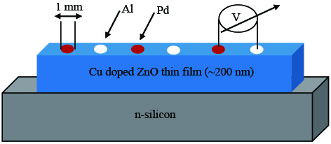
Fig. 1.
(Color?online)?Schematic view of the Pd contact Cu-doped ZnO Schottky diode on n-Si.
SEMICONDUCTOR DEVICES
Lucky Agarwal1, Shweta Tripathi1, and P. Chakrabarti2
Corresponding author: Shweta Tripathi, E-mail: shtri@mnnit.ac.in
Abstract: A systematic study of the behaviour of Pd/p-ZnO thin film Schottky diode has been reported. The p-type ZnO thin film with improved stability has been grown on n-type Si by doping ZnO with copper. Seebeck measurement confirmed the p-type nature of Cu-doped ZnO thin film. The X-ray diffraction spectra of the deposited film revealed polycrystalline nature with preferred growth orientation of (101) of ZnO film. The surface morphological study demonstrated the conformal deposition of a thin film over n-Si wafer. The estimated bandgap of Cu-doped p-type ZnO thin film from ellipsometric measurement turns out to be 3.14 eV at 300 K. The measured electrical parameters of the proposed Pd/p-ZnO Schottky diode have also been validated by the results of numerical simulation obtained by using ATLASTM device simulator.
Key words: p-type ZnO, Cu-doped ZnO, sol-gel method, Schottky diode
| [1] |
Morko? H, ?zgür ü. Zinc oxide: fundamentals, materials and device technology. John Wiley & Sons, 2008
|
| [2] |
Sharma S, Periasamy C, Chakrabarti P. Thickness dependent study of RF sputtered ZnO thin films for optoelectronic device applications. Electron Mater Lett, 2015, 11(6): 1093 doi: 10.1007/s13391-015-4445-y
|
| [3] |
Periasamy C, Chakrabarti P. Time-dependent degradation of Pt/ZnO nanoneedle rectifying contact based piezoelectric nanogenerator. J Appl Phys, 2011, 109(5): 054306 doi: 10.1063/1.3553862
|
| [4] |
Singh BK, Tripathi S. Influence of Bi concentration on structural and optical properties of Bi doped p-type ZnO thin films prepared by sol–gel method. J Mater Scis, 2016, 27(3): 2360
|
| [5] |
Aoki T, Shimizu Y, Miyake A, et al. p-type ZnO layer formation by excimer laser doping. Phys Status Solidi B, 2002, 229(2): 911 doi: 10.1002/(ISSN)1521-3951
|
| [6] |
Snure M, Tiwari A. Band-gap engineering of Zn1-xGaxO nanopowders: synthesis, structural and optical characterizations. J Appl Phys, 2008, 104(7): 73707 doi: 10.1063/1.2988131
|
| [7] |
Xiu FX, Yang Z, Mandalapu LJ, et al. High-mobility Sb-doped p-type ZnO by molecular-beam epitaxy. Appl Phys Lett, 2005, 87(15): 152101 doi: 10.1063/1.2089183
|
| [8] |
Miao Y, Ye Z, Xu W, et al. p-type conduction in phosphorus-doped ZnO thin films by MOCVD and thermal activation of the dopant. Appl Surf Sci, 2006. 252(22): 7953 doi: 10.1016/j.apsusc.2005.10.001
|
| [9] |
Shen Y, Hu W, Zhang T, et al. Arsenic-doped ZnO films fabricated on silicon substrates by pulsed laser ablation. Mater Sci Eng A, 2008, 473(1): 201
|
| [10] |
Mosbacker H L, Strzhemechny Y M, White B D, et al. Role of near-surface states in ohmic-Schottky conversion of Au contacts to ZnO. Appl Phys Lett, 2005, 87(1): 012102 doi: 10.1063/1.1984089
|
| [11] |
West C, Robbins D J, Dean P J, et al. The luminescence of copper in zinc oxide. Physica B + C, 1983, 116(1): 492
|
| [12] |
Wei SH, Li J, Yan Y. Design of shallow p-type dopants in ZnO. IEEE Photovoltaic Specialists Conference, 2008: 1
|
| [13] |
Kim G H, Kim D L, Du A B, et al. Investigation on doping behavior of copper in ZnO thin film. Microelectron J, 2009, 40(2): 272 doi: 10.1016/j.mejo.2008.07.057
|
| [14] |
Agarwal L, Singh B K, Tripathi S, et al. Fabrication and characterization of Pd/Cu doped ZnO/Si and Ni/Cu doped ZnO/Si Schottky diodes. Thin Solid Films, 2016, 612: 259 doi: 10.1016/j.tsf.2016.06.027
|
| [15] |
Xu F, Yuan Z Y, Du G H, et al. Simple approach to highly oriented ZnO nanowire arrays: large-scale growth, photoluminescence and photocatalytic properties. Nanotechnology, 2006, 17(2): 588 doi: 10.1088/0957-4484/17/2/041
|
| [16] |
Rahmani M B, Keshmiri S H, Shafiei M, et al. Transition from n- to p-type of spray pyrolysis deposited Cu doped ZnO thin films for NO2 sensing. Sens Lett, 2009, 7(4): 621 doi: 10.1166/sl.2009.1121
|
| [17] |
Zhang Y D, Wang L W, Mi L W, et al. Silica-controlled structure and optical properties of zinc oxide sol–gel thin films. J Mater Res, 2011, 26(07): 882 doi: 10.1557/jmr.2011.7
|
| [18] |
Bah?i Z B, Oral A Y. Effects of Mn and Cu doping on the microstructures and optical properties of sol–gel derived ZnO thin films. Opt Mater, 2007, 29(6): 672 doi: 10.1016/j.optmat.2005.11.016
|
| [19] |
Jongnavakit P, Amornpitoksuk P, Suwanboon S, et al. Photocatalytic activity of Cu-doped ZnO thin films prepared by the sol–gel method. Appl Surf Sci, 2012, 258(20): 8192 doi: 10.1016/j.apsusc.2012.05.021
|
| [20] |
Neamen, Donald A. Semiconductor physics and devices. McGraw-Hill Higher Education, 2003
|
| [21] |
Kim S, Kang B S, Ren F, et al. Contacts to p-type ZnMgO. Appl Phys Lett, 2004, 84(11): 1904 doi: 10.1063/1.1669082
|
| [22] |
Mandalapu L J, Xiu F X, Yang Z, et al. Al/Ti contacts to Sb-doped p-type ZnO. J Appl Phys, 2007, 102(2): 023716 doi: 10.1063/1.2759874
|
| [23] |
Singh B K, Tripathi S. Fabrication and characterization of Au/p-ZnO Schottky contacts. Superlattices Microstruct, 2015, 85: 697 doi: 10.1016/j.spmi.2015.06.038
|
| [24] |
The International Centre for Diffraction Data, Zincite JCPDS No. 036-1451
|
| [25] |
Yang S, Zhang Y, Mo D. Spectroscopic ellipsometry studies of sol–gel-derived Cu-doped ZnO thin films. Thin Solid Films, 2014, 571: 605 doi: 10.1016/j.tsf.2014.02.097
|
| [26] |
El Sayed AM, Taha S, Said G, et al. Structural and optical properties of spin coated Zn1-xCrxO nanostructures. Superlattices Microstruct, 2013, 60: 108 doi: 10.1016/j.spmi.2013.04.025
|
| [27] |
Ahrens L H. The use of ionization potentials Part 1. Ionic radii of the elements. Geochimica et cosmochimica Acta, 1952, 2(3): 155 doi: 10.1016/0016-7037(52)90004-5
|
| [28] |
Xing G Z, Yao B, Cong C X, et al. Effect of annealing on conductivity behavior of undoped zinc oxide prepared by rf magnetron sputtering. J Alloys Compd, 2008, 457(1): 36
|
| [29] |
Caglar Y, Aksoy S, Ilican S, et al. Crystalline structure and morphological properties of undoped and Sn doped ZnO thin films. Superlattices Microstruct, 2009, 46(3): 469 doi: 10.1016/j.spmi.2009.05.005
|
| [30] |
Shewale P S, Patil V B, Shin S W, et al. H2S gas sensing properties of nanocrystalline Cu-doped ZnO thin films prepared by advanced spray pyrolysis. Sens Actuators B, 2013, 186: 226 doi: 10.1016/j.snb.2013.05.073
|
| [31] |
Muthukumaran S, Gopalakrishnan R. Structural, FTIR and photoluminescence studies of Cu doped ZnO nanopowders by co-precipitation method. Opt Mater, 2012, 34(11): 1946 doi: 10.1016/j.optmat.2012.06.004
|
| [32] |
Hsu C H, Chen L C, Zhang X. Effect of the Cu source on optical properties of Cu ZnO films deposited by ultrasonic spraying. Materials, 2014, 7(2): 1261 doi: 10.3390/ma7021261
|
| [33] |
Zhou S M, Zhang X H, Meng X M, et al. The fabrication and optical properties of highly crystalline ultra-long Cu-doped ZnO nanowires. Nanotechnology, 2004, 15(9): 1152 doi: 10.1088/0957-4484/15/9/007
|
| [34] |
Ahn K S, Deutsch T, Yan Y, et al. Synthesis of band-gap-reduced p-type ZnO films by Cu incorporation. J Appl Phys, 2007, 102(2): 23517 doi: 10.1063/1.2756517
|
| [35] |
Hartnagel H L, Dawar A L, Jain A K, et al. Semiconducting transparent thin films. Bristol: Institute of Physics, 1995
|
| [36] |
Keskenler EF, Aydin S, Turgut G, Do?an S. Optical and structural properties of bismuth doped ZnO thin films by sol–gel method: Urbach rule as a function of crystal defects. Acta Phys Polonica A, 2014, 126(3): 782 doi: 10.12693/APhysPolA.126.782
|
| [37] |
Reddy K R, Reddy T B, Forbes I, et al. Highly oriented and conducting ZnO: Ga layers grown by chemical spray pyrolysis. Surf Coat Technol, 2002, 151: 110
|
| [38] |
Kanai Y. Admittance spectroscopy of Cu-doped ZnO crystals. Jpn J Appl Phys, 1991, 30(4R): 703
|
| [39] |
Pankove J I. Optical processes in semiconductors. Courier Corporation, 2012 Dec 19
|
| [40] |
Alarawi A. Structural and optical properties of Eu doped ZnO nanorods prepared by pulsed laser deposition. Doctoral Dissertation, 2014
|
| [41] |
Asghar M, Mahmood K, Hasan M A. Effect of substrate temperature on the structural and electrical properties of MBE grown ZnO. InKey Eng Mater, 2012, 510: 132
|
| [42] |
Derrouiche S, Lauron-Pernot H, Louis C. Synthesis and treatment parameters for controlling metal particle size and composition in Cu/ZnO materials first evidence of Cu3Zn alloy formation. Chem Mater, 2012, 24(12): 2282 doi: 10.1021/cm3001915
|
| [43] |
Mead C A. Metal–semiconductor surface barriers. Solid-State Electron, 1966, 9(11/12): 1023
|
| [44] |
JWerner J H, Güttler H H. Barrier inhomogeneities at Schottky contacts. J Appl Phys, 1991, 69(3): 1522 doi: 10.1063/1.347243
|
| [45] |
Somvanshi D, Jit S. Analysis of I–V characteristics of Pd/ZnO thin film/n-Si schottky diodes with series resistance. J Nanoelectron Optoelectron, 2014, 9(1): 21 doi: 10.1166/jno.2014.1543
|
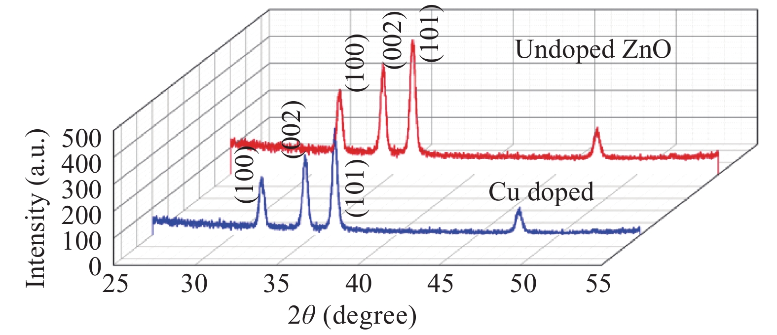
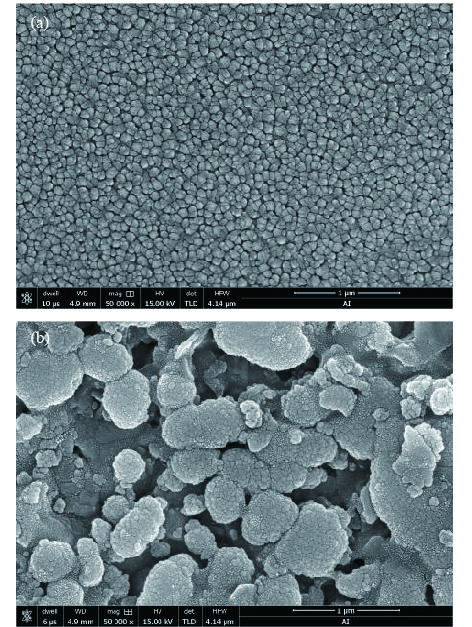
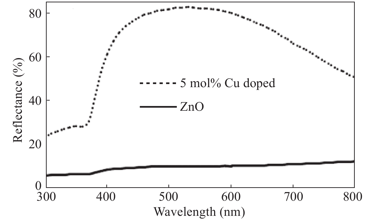
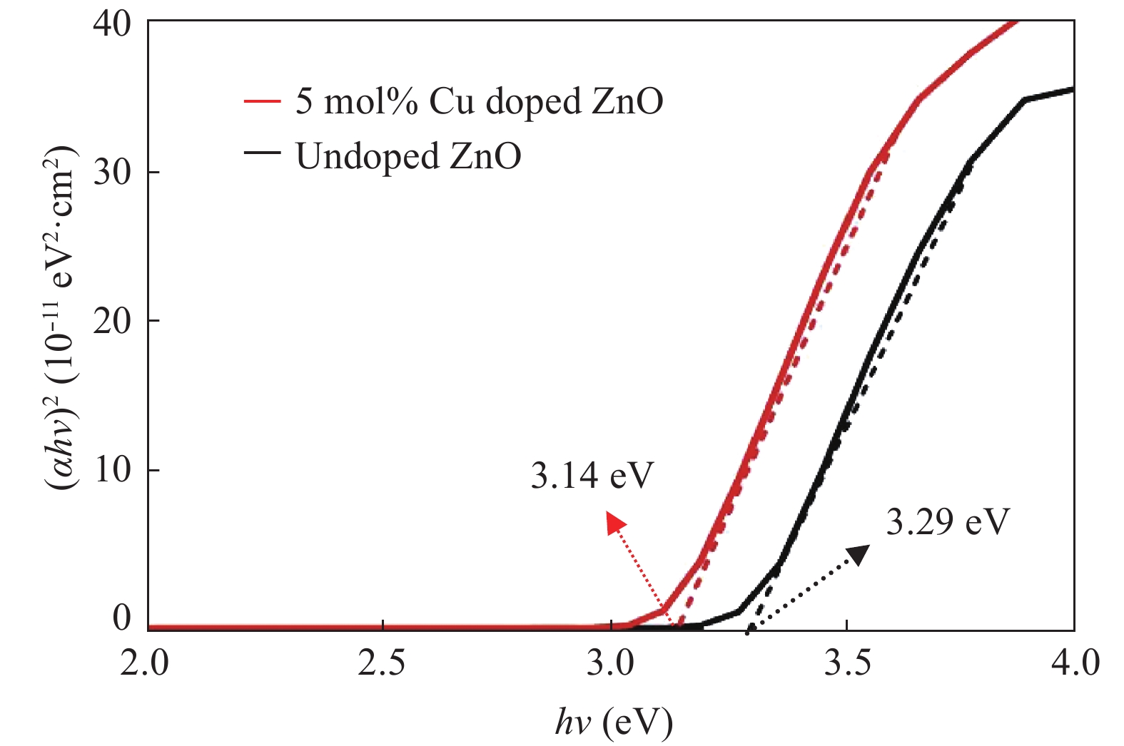
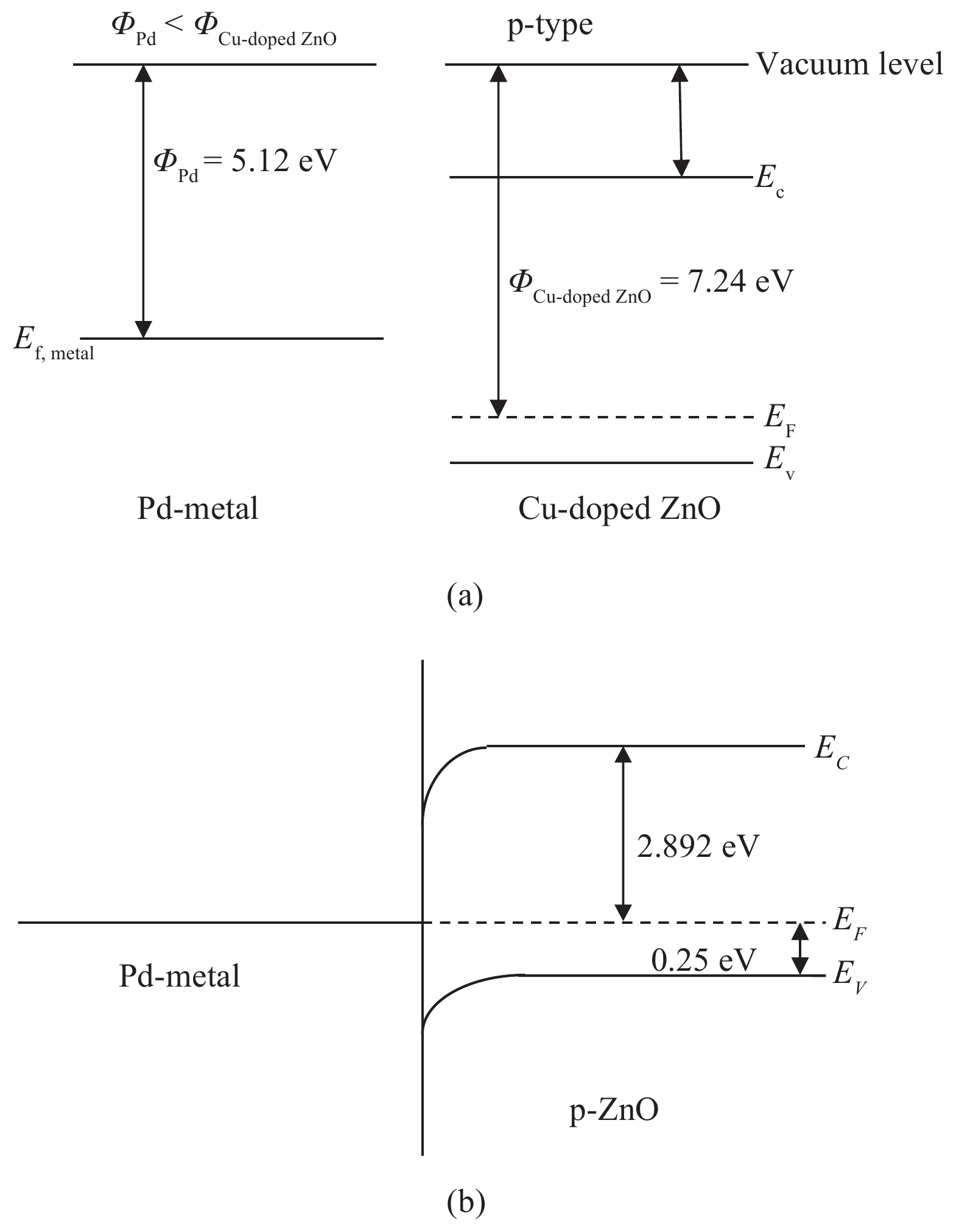
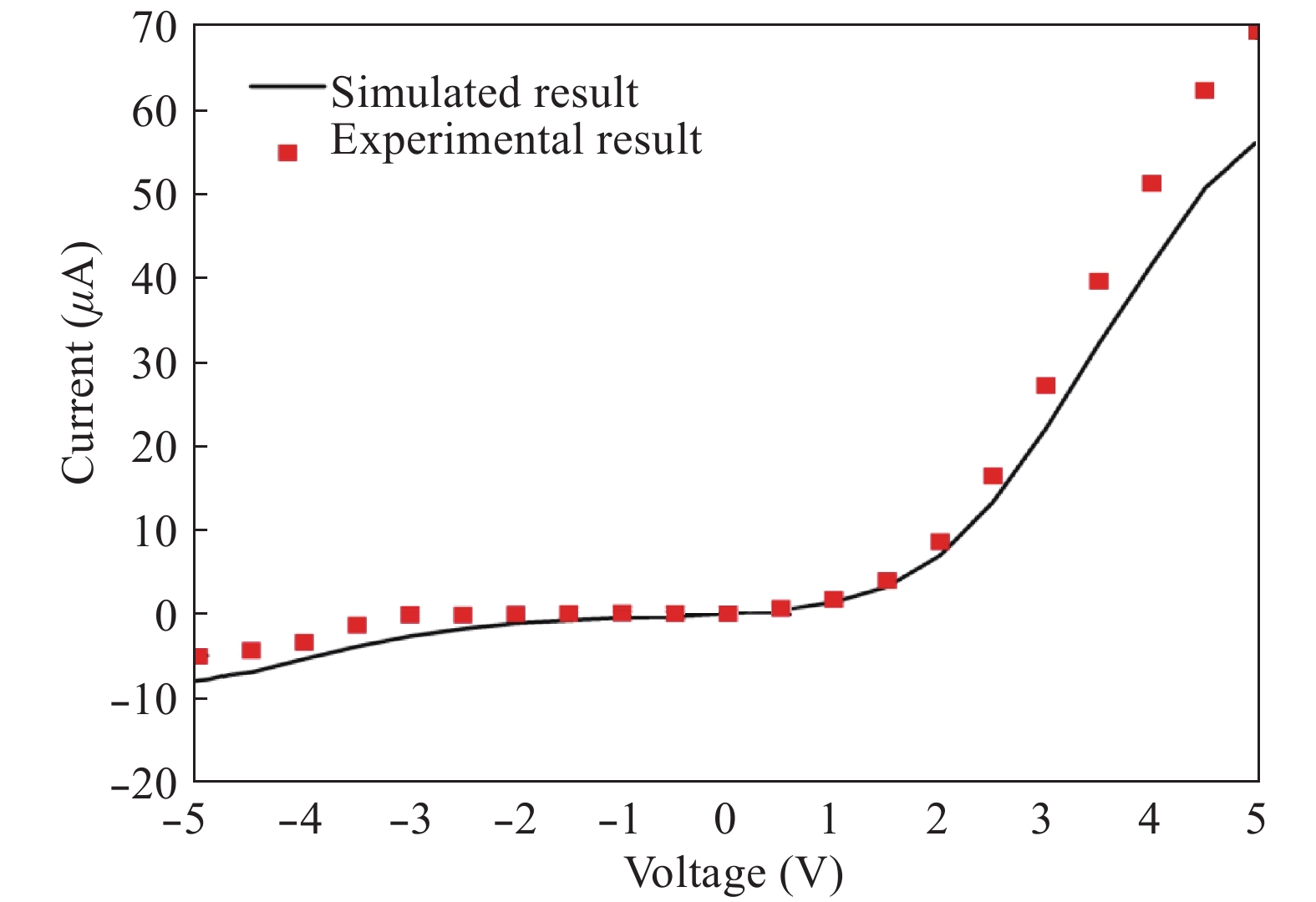
Table 1. Inter planar distance for major orientations and lattice constants value calculated from XRD data.
| Sample | 2θ (101) | Max intensity | Bonding length L (?) | Crystal size D (nm) | FWHM |
| ZnO | 36.29 | 540 | 1.975 72 | 50.04 | 0.44 |
| ZnO:5 mol% Cu | 36.34 | 380 | 1.955 40 | 29.36 | 0.52 |
 DownLoad: CSV
Table 2. Electrical parameters of the fabricated device.
| Device | Reverse saturation current (A) | Barrier height (eV) | Ideality factor | Rectification ratio |
| Experimental (Pd/p-ZnO/n-Si) | 4.57 × 10 –8 | 0.685 | 2.08 | 1189 |
| Simulated | 2.29 × 10 –10 | 0.692 | 2.12 | 1073 |
| Experimental[14] (Pd/p-ZnO/p-Si) | 1.26 × 10 –10 | 0.79 | 2.2 | 995 |
DownLoad: CSV
| [1] |
Morko? H, ?zgür ü. Zinc oxide: fundamentals, materials and device technology. John Wiley & Sons, 2008
|
| [2] |
Sharma S, Periasamy C, Chakrabarti P. Thickness dependent study of RF sputtered ZnO thin films for optoelectronic device applications. Electron Mater Lett, 2015, 11(6): 1093 doi: 10.1007/s13391-015-4445-y
|
| [3] |
Periasamy C, Chakrabarti P. Time-dependent degradation of Pt/ZnO nanoneedle rectifying contact based piezoelectric nanogenerator. J Appl Phys, 2011, 109(5): 054306 doi: 10.1063/1.3553862
|
| [4] |
Singh BK, Tripathi S. Influence of Bi concentration on structural and optical properties of Bi doped p-type ZnO thin films prepared by sol–gel method. J Mater Scis, 2016, 27(3): 2360
|
| [5] |
Aoki T, Shimizu Y, Miyake A, et al. p-type ZnO layer formation by excimer laser doping. Phys Status Solidi B, 2002, 229(2): 911 doi: 10.1002/(ISSN)1521-3951
|
| [6] |
Snure M, Tiwari A. Band-gap engineering of Zn1-xGaxO nanopowders: synthesis, structural and optical characterizations. J Appl Phys, 2008, 104(7): 73707 doi: 10.1063/1.2988131
|
| [7] |
Xiu FX, Yang Z, Mandalapu LJ, et al. High-mobility Sb-doped p-type ZnO by molecular-beam epitaxy. Appl Phys Lett, 2005, 87(15): 152101 doi: 10.1063/1.2089183
|
| [8] |
Miao Y, Ye Z, Xu W, et al. p-type conduction in phosphorus-doped ZnO thin films by MOCVD and thermal activation of the dopant. Appl Surf Sci, 2006. 252(22): 7953 doi: 10.1016/j.apsusc.2005.10.001
|
| [9] |
Shen Y, Hu W, Zhang T, et al. Arsenic-doped ZnO films fabricated on silicon substrates by pulsed laser ablation. Mater Sci Eng A, 2008, 473(1): 201
|
| [10] |
Mosbacker H L, Strzhemechny Y M, White B D, et al. Role of near-surface states in ohmic-Schottky conversion of Au contacts to ZnO. Appl Phys Lett, 2005, 87(1): 012102 doi: 10.1063/1.1984089
|
| [11] |
West C, Robbins D J, Dean P J, et al. The luminescence of copper in zinc oxide. Physica B + C, 1983, 116(1): 492
|
| [12] |
Wei SH, Li J, Yan Y. Design of shallow p-type dopants in ZnO. IEEE Photovoltaic Specialists Conference, 2008: 1
|
| [13] |
Kim G H, Kim D L, Du A B, et al. Investigation on doping behavior of copper in ZnO thin film. Microelectron J, 2009, 40(2): 272 doi: 10.1016/j.mejo.2008.07.057
|
| [14] |
Agarwal L, Singh B K, Tripathi S, et al. Fabrication and characterization of Pd/Cu doped ZnO/Si and Ni/Cu doped ZnO/Si Schottky diodes. Thin Solid Films, 2016, 612: 259 doi: 10.1016/j.tsf.2016.06.027
|
| [15] |
Xu F, Yuan Z Y, Du G H, et al. Simple approach to highly oriented ZnO nanowire arrays: large-scale growth, photoluminescence and photocatalytic properties. Nanotechnology, 2006, 17(2): 588 doi: 10.1088/0957-4484/17/2/041
|
| [16] |
Rahmani M B, Keshmiri S H, Shafiei M, et al. Transition from n- to p-type of spray pyrolysis deposited Cu doped ZnO thin films for NO2 sensing. Sens Lett, 2009, 7(4): 621 doi: 10.1166/sl.2009.1121
|
| [17] |
Zhang Y D, Wang L W, Mi L W, et al. Silica-controlled structure and optical properties of zinc oxide sol–gel thin films. J Mater Res, 2011, 26(07): 882 doi: 10.1557/jmr.2011.7
|
| [18] |
Bah?i Z B, Oral A Y. Effects of Mn and Cu doping on the microstructures and optical properties of sol–gel derived ZnO thin films. Opt Mater, 2007, 29(6): 672 doi: 10.1016/j.optmat.2005.11.016
|
| [19] |
Jongnavakit P, Amornpitoksuk P, Suwanboon S, et al. Photocatalytic activity of Cu-doped ZnO thin films prepared by the sol–gel method. Appl Surf Sci, 2012, 258(20): 8192 doi: 10.1016/j.apsusc.2012.05.021
|
| [20] |
Neamen, Donald A. Semiconductor physics and devices. McGraw-Hill Higher Education, 2003
|
| [21] |
Kim S, Kang B S, Ren F, et al. Contacts to p-type ZnMgO. Appl Phys Lett, 2004, 84(11): 1904 doi: 10.1063/1.1669082
|
| [22] |
Mandalapu L J, Xiu F X, Yang Z, et al. Al/Ti contacts to Sb-doped p-type ZnO. J Appl Phys, 2007, 102(2): 023716 doi: 10.1063/1.2759874
|
| [23] |
Singh B K, Tripathi S. Fabrication and characterization of Au/p-ZnO Schottky contacts. Superlattices Microstruct, 2015, 85: 697 doi: 10.1016/j.spmi.2015.06.038
|
| [24] |
The International Centre for Diffraction Data, Zincite JCPDS No. 036-1451
|
| [25] |
Yang S, Zhang Y, Mo D. Spectroscopic ellipsometry studies of sol–gel-derived Cu-doped ZnO thin films. Thin Solid Films, 2014, 571: 605 doi: 10.1016/j.tsf.2014.02.097
|
| [26] |
El Sayed AM, Taha S, Said G, et al. Structural and optical properties of spin coated Zn1-xCrxO nanostructures. Superlattices Microstruct, 2013, 60: 108 doi: 10.1016/j.spmi.2013.04.025
|
| [27] |
Ahrens L H. The use of ionization potentials Part 1. Ionic radii of the elements. Geochimica et cosmochimica Acta, 1952, 2(3): 155 doi: 10.1016/0016-7037(52)90004-5
|
| [28] |
Xing G Z, Yao B, Cong C X, et al. Effect of annealing on conductivity behavior of undoped zinc oxide prepared by rf magnetron sputtering. J Alloys Compd, 2008, 457(1): 36
|
| [29] |
Caglar Y, Aksoy S, Ilican S, et al. Crystalline structure and morphological properties of undoped and Sn doped ZnO thin films. Superlattices Microstruct, 2009, 46(3): 469 doi: 10.1016/j.spmi.2009.05.005
|
| [30] |
Shewale P S, Patil V B, Shin S W, et al. H2S gas sensing properties of nanocrystalline Cu-doped ZnO thin films prepared by advanced spray pyrolysis. Sens Actuators B, 2013, 186: 226 doi: 10.1016/j.snb.2013.05.073
|
| [31] |
Muthukumaran S, Gopalakrishnan R. Structural, FTIR and photoluminescence studies of Cu doped ZnO nanopowders by co-precipitation method. Opt Mater, 2012, 34(11): 1946 doi: 10.1016/j.optmat.2012.06.004
|
| [32] |
Hsu C H, Chen L C, Zhang X. Effect of the Cu source on optical properties of Cu ZnO films deposited by ultrasonic spraying. Materials, 2014, 7(2): 1261 doi: 10.3390/ma7021261
|
| [33] |
Zhou S M, Zhang X H, Meng X M, et al. The fabrication and optical properties of highly crystalline ultra-long Cu-doped ZnO nanowires. Nanotechnology, 2004, 15(9): 1152 doi: 10.1088/0957-4484/15/9/007
|
| [34] |
Ahn K S, Deutsch T, Yan Y, et al. Synthesis of band-gap-reduced p-type ZnO films by Cu incorporation. J Appl Phys, 2007, 102(2): 23517 doi: 10.1063/1.2756517
|
| [35] |
Hartnagel H L, Dawar A L, Jain A K, et al. Semiconducting transparent thin films. Bristol: Institute of Physics, 1995
|
| [36] |
Keskenler EF, Aydin S, Turgut G, Do?an S. Optical and structural properties of bismuth doped ZnO thin films by sol–gel method: Urbach rule as a function of crystal defects. Acta Phys Polonica A, 2014, 126(3): 782 doi: 10.12693/APhysPolA.126.782
|
| [37] |
Reddy K R, Reddy T B, Forbes I, et al. Highly oriented and conducting ZnO: Ga layers grown by chemical spray pyrolysis. Surf Coat Technol, 2002, 151: 110
|
| [38] |
Kanai Y. Admittance spectroscopy of Cu-doped ZnO crystals. Jpn J Appl Phys, 1991, 30(4R): 703
|
| [39] |
Pankove J I. Optical processes in semiconductors. Courier Corporation, 2012 Dec 19
|
| [40] |
Alarawi A. Structural and optical properties of Eu doped ZnO nanorods prepared by pulsed laser deposition. Doctoral Dissertation, 2014
|
| [41] |
Asghar M, Mahmood K, Hasan M A. Effect of substrate temperature on the structural and electrical properties of MBE grown ZnO. InKey Eng Mater, 2012, 510: 132
|
| [42] |
Derrouiche S, Lauron-Pernot H, Louis C. Synthesis and treatment parameters for controlling metal particle size and composition in Cu/ZnO materials first evidence of Cu3Zn alloy formation. Chem Mater, 2012, 24(12): 2282 doi: 10.1021/cm3001915
|
| [43] |
Mead C A. Metal–semiconductor surface barriers. Solid-State Electron, 1966, 9(11/12): 1023
|
| [44] |
JWerner J H, Güttler H H. Barrier inhomogeneities at Schottky contacts. J Appl Phys, 1991, 69(3): 1522 doi: 10.1063/1.347243
|
| [45] |
Somvanshi D, Jit S. Analysis of I–V characteristics of Pd/ZnO thin film/n-Si schottky diodes with series resistance. J Nanoelectron Optoelectron, 2014, 9(1): 21 doi: 10.1166/jno.2014.1543
|


Article views: 4451 Times PDF downloads: 54 Times Cited by: 0 Times
Received: 14 January 2017 Revised: 12 May 2017 Online: Accepted Manuscript: 13 November 2017Published: 01 October 2017
| Citation: |
Lucky Agarwal, Shweta Tripathi, P. Chakrabarti. Analysis of structural, optical and electrical properties of metal/p-ZnO-based Schottky diode[J]. Journal of Semiconductors, 2017, 38(10): 104002. doi: 10.1088/1674-4926/38/10/104002
****
L Agarwal, S Tripathi, P. Chakrabarti. Analysis of structural, optical and electrical properties of metal/p-ZnO-based Schottky diode[J]. J. Semicond., 2017, 38(10): 104002. doi: 10.1088/1674-4926/38/10/104002.

|
| [1] |
Morko? H, ?zgür ü. Zinc oxide: fundamentals, materials and device technology. John Wiley & Sons, 2008
|
| [2] |
Sharma S, Periasamy C, Chakrabarti P. Thickness dependent study of RF sputtered ZnO thin films for optoelectronic device applications. Electron Mater Lett, 2015, 11(6): 1093 doi: 10.1007/s13391-015-4445-y
|
| [3] |
Periasamy C, Chakrabarti P. Time-dependent degradation of Pt/ZnO nanoneedle rectifying contact based piezoelectric nanogenerator. J Appl Phys, 2011, 109(5): 054306 doi: 10.1063/1.3553862
|
| [4] |
Singh BK, Tripathi S. Influence of Bi concentration on structural and optical properties of Bi doped p-type ZnO thin films prepared by sol–gel method. J Mater Scis, 2016, 27(3): 2360
|
| [5] |
Aoki T, Shimizu Y, Miyake A, et al. p-type ZnO layer formation by excimer laser doping. Phys Status Solidi B, 2002, 229(2): 911 doi: 10.1002/(ISSN)1521-3951
|
| [6] |
Snure M, Tiwari A. Band-gap engineering of Zn1-xGaxO nanopowders: synthesis, structural and optical characterizations. J Appl Phys, 2008, 104(7): 73707 doi: 10.1063/1.2988131
|
| [7] |
Xiu FX, Yang Z, Mandalapu LJ, et al. High-mobility Sb-doped p-type ZnO by molecular-beam epitaxy. Appl Phys Lett, 2005, 87(15): 152101 doi: 10.1063/1.2089183
|
| [8] |
Miao Y, Ye Z, Xu W, et al. p-type conduction in phosphorus-doped ZnO thin films by MOCVD and thermal activation of the dopant. Appl Surf Sci, 2006. 252(22): 7953 doi: 10.1016/j.apsusc.2005.10.001
|
| [9] |
Shen Y, Hu W, Zhang T, et al. Arsenic-doped ZnO films fabricated on silicon substrates by pulsed laser ablation. Mater Sci Eng A, 2008, 473(1): 201
|
| [10] |
Mosbacker H L, Strzhemechny Y M, White B D, et al. Role of near-surface states in ohmic-Schottky conversion of Au contacts to ZnO. Appl Phys Lett, 2005, 87(1): 012102 doi: 10.1063/1.1984089
|
| [11] |
West C, Robbins D J, Dean P J, et al. The luminescence of copper in zinc oxide. Physica B + C, 1983, 116(1): 492
|
| [12] |
Wei SH, Li J, Yan Y. Design of shallow p-type dopants in ZnO. IEEE Photovoltaic Specialists Conference, 2008: 1
|
| [13] |
Kim G H, Kim D L, Du A B, et al. Investigation on doping behavior of copper in ZnO thin film. Microelectron J, 2009, 40(2): 272 doi: 10.1016/j.mejo.2008.07.057
|
| [14] |
Agarwal L, Singh B K, Tripathi S, et al. Fabrication and characterization of Pd/Cu doped ZnO/Si and Ni/Cu doped ZnO/Si Schottky diodes. Thin Solid Films, 2016, 612: 259 doi: 10.1016/j.tsf.2016.06.027
|
| [15] |
Xu F, Yuan Z Y, Du G H, et al. Simple approach to highly oriented ZnO nanowire arrays: large-scale growth, photoluminescence and photocatalytic properties. Nanotechnology, 2006, 17(2): 588 doi: 10.1088/0957-4484/17/2/041
|
| [16] |
Rahmani M B, Keshmiri S H, Shafiei M, et al. Transition from n- to p-type of spray pyrolysis deposited Cu doped ZnO thin films for NO2 sensing. Sens Lett, 2009, 7(4): 621 doi: 10.1166/sl.2009.1121
|
| [17] |
Zhang Y D, Wang L W, Mi L W, et al. Silica-controlled structure and optical properties of zinc oxide sol–gel thin films. J Mater Res, 2011, 26(07): 882 doi: 10.1557/jmr.2011.7
|
| [18] |
Bah?i Z B, Oral A Y. Effects of Mn and Cu doping on the microstructures and optical properties of sol–gel derived ZnO thin films. Opt Mater, 2007, 29(6): 672 doi: 10.1016/j.optmat.2005.11.016
|
| [19] |
Jongnavakit P, Amornpitoksuk P, Suwanboon S, et al. Photocatalytic activity of Cu-doped ZnO thin films prepared by the sol–gel method. Appl Surf Sci, 2012, 258(20): 8192 doi: 10.1016/j.apsusc.2012.05.021
|
| [20] |
Neamen, Donald A. Semiconductor physics and devices. McGraw-Hill Higher Education, 2003
|
| [21] |
Kim S, Kang B S, Ren F, et al. Contacts to p-type ZnMgO. Appl Phys Lett, 2004, 84(11): 1904 doi: 10.1063/1.1669082
|
| [22] |
Mandalapu L J, Xiu F X, Yang Z, et al. Al/Ti contacts to Sb-doped p-type ZnO. J Appl Phys, 2007, 102(2): 023716 doi: 10.1063/1.2759874
|
| [23] |
Singh B K, Tripathi S. Fabrication and characterization of Au/p-ZnO Schottky contacts. Superlattices Microstruct, 2015, 85: 697 doi: 10.1016/j.spmi.2015.06.038
|
| [24] |
The International Centre for Diffraction Data, Zincite JCPDS No. 036-1451
|
| [25] |
Yang S, Zhang Y, Mo D. Spectroscopic ellipsometry studies of sol–gel-derived Cu-doped ZnO thin films. Thin Solid Films, 2014, 571: 605 doi: 10.1016/j.tsf.2014.02.097
|
| [26] |
El Sayed AM, Taha S, Said G, et al. Structural and optical properties of spin coated Zn1-xCrxO nanostructures. Superlattices Microstruct, 2013, 60: 108 doi: 10.1016/j.spmi.2013.04.025
|
| [27] |
Ahrens L H. The use of ionization potentials Part 1. Ionic radii of the elements. Geochimica et cosmochimica Acta, 1952, 2(3): 155 doi: 10.1016/0016-7037(52)90004-5
|
| [28] |
Xing G Z, Yao B, Cong C X, et al. Effect of annealing on conductivity behavior of undoped zinc oxide prepared by rf magnetron sputtering. J Alloys Compd, 2008, 457(1): 36
|
| [29] |
Caglar Y, Aksoy S, Ilican S, et al. Crystalline structure and morphological properties of undoped and Sn doped ZnO thin films. Superlattices Microstruct, 2009, 46(3): 469 doi: 10.1016/j.spmi.2009.05.005
|
| [30] |
Shewale P S, Patil V B, Shin S W, et al. H2S gas sensing properties of nanocrystalline Cu-doped ZnO thin films prepared by advanced spray pyrolysis. Sens Actuators B, 2013, 186: 226 doi: 10.1016/j.snb.2013.05.073
|
| [31] |
Muthukumaran S, Gopalakrishnan R. Structural, FTIR and photoluminescence studies of Cu doped ZnO nanopowders by co-precipitation method. Opt Mater, 2012, 34(11): 1946 doi: 10.1016/j.optmat.2012.06.004
|
| [32] |
Hsu C H, Chen L C, Zhang X. Effect of the Cu source on optical properties of Cu ZnO films deposited by ultrasonic spraying. Materials, 2014, 7(2): 1261 doi: 10.3390/ma7021261
|
| [33] |
Zhou S M, Zhang X H, Meng X M, et al. The fabrication and optical properties of highly crystalline ultra-long Cu-doped ZnO nanowires. Nanotechnology, 2004, 15(9): 1152 doi: 10.1088/0957-4484/15/9/007
|
| [34] |
Ahn K S, Deutsch T, Yan Y, et al. Synthesis of band-gap-reduced p-type ZnO films by Cu incorporation. J Appl Phys, 2007, 102(2): 23517 doi: 10.1063/1.2756517
|
| [35] |
Hartnagel H L, Dawar A L, Jain A K, et al. Semiconducting transparent thin films. Bristol: Institute of Physics, 1995
|
| [36] |
Keskenler EF, Aydin S, Turgut G, Do?an S. Optical and structural properties of bismuth doped ZnO thin films by sol–gel method: Urbach rule as a function of crystal defects. Acta Phys Polonica A, 2014, 126(3): 782 doi: 10.12693/APhysPolA.126.782
|
| [37] |
Reddy K R, Reddy T B, Forbes I, et al. Highly oriented and conducting ZnO: Ga layers grown by chemical spray pyrolysis. Surf Coat Technol, 2002, 151: 110
|
| [38] |
Kanai Y. Admittance spectroscopy of Cu-doped ZnO crystals. Jpn J Appl Phys, 1991, 30(4R): 703
|
| [39] |
Pankove J I. Optical processes in semiconductors. Courier Corporation, 2012 Dec 19
|
| [40] |
Alarawi A. Structural and optical properties of Eu doped ZnO nanorods prepared by pulsed laser deposition. Doctoral Dissertation, 2014
|
| [41] |
Asghar M, Mahmood K, Hasan M A. Effect of substrate temperature on the structural and electrical properties of MBE grown ZnO. InKey Eng Mater, 2012, 510: 132
|
| [42] |
Derrouiche S, Lauron-Pernot H, Louis C. Synthesis and treatment parameters for controlling metal particle size and composition in Cu/ZnO materials first evidence of Cu3Zn alloy formation. Chem Mater, 2012, 24(12): 2282 doi: 10.1021/cm3001915
|
| [43] |
Mead C A. Metal–semiconductor surface barriers. Solid-State Electron, 1966, 9(11/12): 1023
|
| [44] |
JWerner J H, Güttler H H. Barrier inhomogeneities at Schottky contacts. J Appl Phys, 1991, 69(3): 1522 doi: 10.1063/1.347243
|
| [45] |
Somvanshi D, Jit S. Analysis of I–V characteristics of Pd/ZnO thin film/n-Si schottky diodes with series resistance. J Nanoelectron Optoelectron, 2014, 9(1): 21 doi: 10.1166/jno.2014.1543
|

 WeChat ID
Journal of Semiconductors © 2017 All Rights Reserved 京ICP備05085259號-2

