


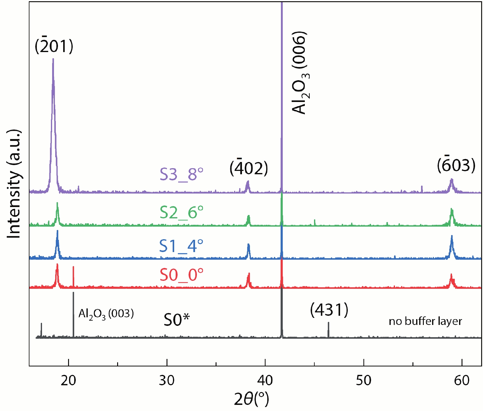
Fig. 1.
(Color online) XRD patterns of β-Ga2O3 films deposited on c-plane Al2O3 substrates with different off-axis angles toward <$11\bar{2}0 $ >.
ARTICLES
Yabao Zhang1, 2, Jun Zheng1, 2, , Peipei Ma1, 2, Xueyi Zheng1, 3, Zhi Liu1, 2, Yuhua Zuo1, 2, Chuanbo Li3 and Buwen Cheng1, 2
Corresponding author: Jun Zheng, zhengjun@semi.ac.cn
Abstract: Beta-gallium oxide (β-Ga2O3) thin films were deposited on c-plane (0001) sapphire substrates with different mis-cut angles along <
Key words: β-Ga2O3, heteroepitaxy, mis-cut Al2O3 substrates, MOCVD
| [1] |
Jeong Y J, Yang J Y, Lee C H, et al. Fluorine-based plasma treatment for hetero-epitaxial β-Ga2O3 MOSFETs. Appl Surf Sci, 2021, 558, 149936 doi: 10.1016/j.apsusc.2021.149936
|
| [2] |
Jubu P R, Yam F K. Development and characterization of MSM UV photodetector based on gallium oxide nanostructures. Sens Actuator A, 2020, 312, 112141 doi: 10.1016/j.sna.2020.112141
|
| [3] |
Lv Y J, Zhou X Y, Long S B, et al. Enhancement-mode β-Ga2O3 metal-oxide-semiconductor field-effect transistor with high breakdown voltage over 3000 V realized by oxygen annealing. Phys Status Solidi RRL, 2020, 14, 1900586 doi: 10.1002/pssr.201900586
|
| [4] |
Dong H, Xue H W, He Q M, et al. Progress of power field effect transistor based on ultra-wide bandgap Ga2O3 semiconductor material. J Semicond, 2019, 40, 011802 doi: 10.1088/1674-4926/40/1/011802
|
| [5] |
Tippins H H. Optical absorption and photoconductivity in the band edge of β-Ga2O3. Phys Rev, 1965, 140, A316 doi: 10.1103/PhysRev.140.A316
|
| [6] |
Ueda N, Hosono H, Waseda R, et al. Anisotropy of electrical and optical properties in β-Ga2O3 single crystals. Appl Phys Lett, 1997, 71, 933 doi: 10.1063/1.119693
|
| [7] |
Kohn J A, Broder J D. Characterization of β-Ga2O3 and its alumina isomorph, θ-Al2O3. Am Mineral, 1957, 42, 398
|
| [8] |
Stepanov S I, Nikolaev V I, Bougrov V E, et al. Gallium oxide: Properties and applications - A review. Rev Adv Mater Sci, 2016, 44, 63
|
| [9] |
Pearton S J, Yang J C, Cary P H, et al. A review of Ga2O3 materials, processing, and devices. Appl Phys Rev, 2018, 5, 011301 doi: 10.1063/1.5006941
|
| [10] |
Wang D, He L N, Le Y, et al. Characterization of single crystal β-Ga2O3 films grown on SrTiO3 (100) substrates by MOCVD. Ceram Int, 2020, 46, 4568 doi: 10.1016/j.ceramint.2019.10.185
|
| [11] |
Cao Q, He L N, Xiao H D, et al. β-Ga2O3 epitaxial films deposited on epi-GaN/sapphire (0001) substrates by MOCVD. Mater Sci Semicond Process, 2018, 77, 58 doi: 10.1016/j.mssp.2018.01.010
|
| [12] |
Mi W, Ma J, Luan C N, et al. Characterization of β-Ga2O3 epitaxial films grown on MgO (111) substrates by metal-organic chemical vapor deposition. Mater Lett, 2012, 87, 109 doi: 10.1016/j.matlet.2012.07.106
|
| [13] |
Mi W, Luan C N, Li Z, et al. Ultraviolet-green photoluminescence of β-Ga2O3 films deposited on MgAl6O10 (100) substrate. Opt Mater, 2013, 35, 2624 doi: 10.1016/j.optmat.2013.07.030
|
| [14] |
Qian C, Sun J, Zhang L, et al. Crystal-domain orientation and boundary in highly ordered organic semiconductor thin film. J Phys Chem C, 2015, 119, 14965 doi: 10.1021/acs.jpcc.5b03727
|
| [15] |
Nakagomi S, Kokubun Y. Crystal orientation of β-Ga2O3 thin films formed on c-plane and a-plane sapphire substrate. J Cryst Growth, 2012, 349, 12 doi: 10.1016/j.jcrysgro.2012.04.006
|
| [16] |
Boschi F, Bosi M, Berzina T, et al. Hetero-epitaxy of ε-Ga2O3 layers by MOCVD and ALD. J Cryst Growth, 2016, 443, 25 doi: 10.1016/j.jcrysgro.2016.03.013
|
| [17] |
Zhuo Y, Chen Z M, Tu W B, et al. β-Ga2O3 versus ε-Ga2O3: Control of the crystal phase composition of gallium oxide thin film prepared by metal-organic chemical vapor deposition. Appl Surf Sci, 2017, 420, 802 doi: 10.1016/j.apsusc.2017.05.241
|
| [18] |
Hu D Q, Wang Y, Zhuang S W, et al. Surface morphology evolution and optoelectronic properties of heteroepitaxial Si-doped β-Ga2O3 thin films grown by metal-organic chemical vapor deposition. Ceram Int, 2018, 44, 3122 doi: 10.1016/j.ceramint.2017.11.079
|
| [19] |
Wu J W, Mi W, Yang Z C, et al. Influence of annealing on the structural and optical properties of gallium oxide films deposited on c-sapphire substrate. Vacuum, 2019, 167, 6 doi: 10.1016/j.vacuum.2019.05.034
|
| [20] |
Wei J Q, Kim K, Liu F, et al. β-Ga2O3 thin film grown on sapphire substrate by plasma-assisted molecular beam epitaxy. J Semicond, 2019, 40, 012802 doi: 10.1088/1674-4926/40/1/012802
|
| [21] |
Oshima Y, V?llora E G, Shimamura K. Quasi-heteroepitaxial growth of β-Ga2O3 on off-angled sapphire (0001) substrates by halide vapor phase epitaxy. J Cryst Growth, 2015, 410, 53 doi: 10.1016/j.jcrysgro.2014.10.038
|
| [22] |
Xu W L, Shi J C, Li Y W, et al. Study of β-Ga2O3 films hetero-epitaxially grown on off-angled sapphire substrates by halide vapor phase epitaxy. Mater Lett, 2021, 289, 129411 doi: 10.1016/j.matlet.2021.129411
|
| [23] |
Rafique S, Han L, Neal A T, et al. Towards high-mobility heteroepitaxial β-Ga2O3 on sapphire–dependence on the substrate off-axis angle. Phys Status Solidi A, 2018, 215, 1700467 doi: 10.1002/pssa.201700467
|
| [24] |
Zhang T, Hu Z G, Li Y F, et al. Investigation on the β-Ga2O3 deposited on off-angled sapphire (0001) substrates. J Lumin, 2021, 233, 117928 doi: 10.1016/j.jlumin.2021.117928
|
| [25] |
Bryan I, Bryan Z, Mita S, et al. Surface kinetics in AlN growth: A universal model for the control of surface morphology in III-nitrides. J Cryst Growth, 2016, 438, 81 doi: 10.1016/j.jcrysgro.2015.12.022
|
| [26] |
Xie M H, Cheung S H, Zheng L X, et al. Step bunching of vicinal GaN(0001) surfaces during molecular beam epitaxy. Phys Rev B, 2000, 61, 9983 doi: 10.1103/PhysRevB.61.9983
|
| [27] |
Varley J B, Janotti A, Franchini C, et al. Role of self-trapping in luminescence andp-type conductivity of wide-band-gap oxides. Phys Rev B, 2012, 85, 081109 doi: 10.1103/PhysRevB.85.081109
|
| [28] |
Ho C H, Tseng C Y, Tien L C. Thermoreflectance characterization of beta-Ga2O3 thin-film nanostrips. Opt Express, 2010, 18, 16360 doi: 10.1364/OE.18.016360
|


Article views: 4847 Times PDF downloads: 578 Times Cited by: 0 Times
Received: 13 January 2022 Revised: 08 April 2022 Online: Accepted Manuscript: 15 May 2022Uncorrected proof: 18 May 2022Published: 02 September 2022
| Citation: |
Yabao Zhang, Jun Zheng, Peipei Ma, Xueyi Zheng, Zhi Liu, Yuhua Zuo, Chuanbo Li, Buwen Cheng. Growth and characterization of β-Ga2O3 thin films grown on off-angled Al2O3 substrates by metal-organic chemical vapor deposition[J]. Journal of Semiconductors, 2022, 43(9): 092801. doi: 10.1088/1674-4926/43/9/092801
****
Y B Zhang, J Zheng, P P Ma, X Y Zheng, Z Liu, Y H Zuo, C B Li, B W Cheng. Growth and characterization of β-Ga2O3 thin films grown on off-angled Al2O3 substrates by metal-organic chemical vapor deposition[J]. J. Semicond, 2022, 43(9): 092801. doi: 10.1088/1674-4926/43/9/092801

|
| [1] |
Jeong Y J, Yang J Y, Lee C H, et al. Fluorine-based plasma treatment for hetero-epitaxial β-Ga2O3 MOSFETs. Appl Surf Sci, 2021, 558, 149936 doi: 10.1016/j.apsusc.2021.149936
|
| [2] |
Jubu P R, Yam F K. Development and characterization of MSM UV photodetector based on gallium oxide nanostructures. Sens Actuator A, 2020, 312, 112141 doi: 10.1016/j.sna.2020.112141
|
| [3] |
Lv Y J, Zhou X Y, Long S B, et al. Enhancement-mode β-Ga2O3 metal-oxide-semiconductor field-effect transistor with high breakdown voltage over 3000 V realized by oxygen annealing. Phys Status Solidi RRL, 2020, 14, 1900586 doi: 10.1002/pssr.201900586
|
| [4] |
Dong H, Xue H W, He Q M, et al. Progress of power field effect transistor based on ultra-wide bandgap Ga2O3 semiconductor material. J Semicond, 2019, 40, 011802 doi: 10.1088/1674-4926/40/1/011802
|
| [5] |
Tippins H H. Optical absorption and photoconductivity in the band edge of β-Ga2O3. Phys Rev, 1965, 140, A316 doi: 10.1103/PhysRev.140.A316
|
| [6] |
Ueda N, Hosono H, Waseda R, et al. Anisotropy of electrical and optical properties in β-Ga2O3 single crystals. Appl Phys Lett, 1997, 71, 933 doi: 10.1063/1.119693
|
| [7] |
Kohn J A, Broder J D. Characterization of β-Ga2O3 and its alumina isomorph, θ-Al2O3. Am Mineral, 1957, 42, 398
|
| [8] |
Stepanov S I, Nikolaev V I, Bougrov V E, et al. Gallium oxide: Properties and applications - A review. Rev Adv Mater Sci, 2016, 44, 63
|
| [9] |
Pearton S J, Yang J C, Cary P H, et al. A review of Ga2O3 materials, processing, and devices. Appl Phys Rev, 2018, 5, 011301 doi: 10.1063/1.5006941
|
| [10] |
Wang D, He L N, Le Y, et al. Characterization of single crystal β-Ga2O3 films grown on SrTiO3 (100) substrates by MOCVD. Ceram Int, 2020, 46, 4568 doi: 10.1016/j.ceramint.2019.10.185
|
| [11] |
Cao Q, He L N, Xiao H D, et al. β-Ga2O3 epitaxial films deposited on epi-GaN/sapphire (0001) substrates by MOCVD. Mater Sci Semicond Process, 2018, 77, 58 doi: 10.1016/j.mssp.2018.01.010
|
| [12] |
Mi W, Ma J, Luan C N, et al. Characterization of β-Ga2O3 epitaxial films grown on MgO (111) substrates by metal-organic chemical vapor deposition. Mater Lett, 2012, 87, 109 doi: 10.1016/j.matlet.2012.07.106
|
| [13] |
Mi W, Luan C N, Li Z, et al. Ultraviolet-green photoluminescence of β-Ga2O3 films deposited on MgAl6O10 (100) substrate. Opt Mater, 2013, 35, 2624 doi: 10.1016/j.optmat.2013.07.030
|
| [14] |
Qian C, Sun J, Zhang L, et al. Crystal-domain orientation and boundary in highly ordered organic semiconductor thin film. J Phys Chem C, 2015, 119, 14965 doi: 10.1021/acs.jpcc.5b03727
|
| [15] |
Nakagomi S, Kokubun Y. Crystal orientation of β-Ga2O3 thin films formed on c-plane and a-plane sapphire substrate. J Cryst Growth, 2012, 349, 12 doi: 10.1016/j.jcrysgro.2012.04.006
|
| [16] |
Boschi F, Bosi M, Berzina T, et al. Hetero-epitaxy of ε-Ga2O3 layers by MOCVD and ALD. J Cryst Growth, 2016, 443, 25 doi: 10.1016/j.jcrysgro.2016.03.013
|
| [17] |
Zhuo Y, Chen Z M, Tu W B, et al. β-Ga2O3 versus ε-Ga2O3: Control of the crystal phase composition of gallium oxide thin film prepared by metal-organic chemical vapor deposition. Appl Surf Sci, 2017, 420, 802 doi: 10.1016/j.apsusc.2017.05.241
|
| [18] |
Hu D Q, Wang Y, Zhuang S W, et al. Surface morphology evolution and optoelectronic properties of heteroepitaxial Si-doped β-Ga2O3 thin films grown by metal-organic chemical vapor deposition. Ceram Int, 2018, 44, 3122 doi: 10.1016/j.ceramint.2017.11.079
|
| [19] |
Wu J W, Mi W, Yang Z C, et al. Influence of annealing on the structural and optical properties of gallium oxide films deposited on c-sapphire substrate. Vacuum, 2019, 167, 6 doi: 10.1016/j.vacuum.2019.05.034
|
| [20] |
Wei J Q, Kim K, Liu F, et al. β-Ga2O3 thin film grown on sapphire substrate by plasma-assisted molecular beam epitaxy. J Semicond, 2019, 40, 012802 doi: 10.1088/1674-4926/40/1/012802
|
| [21] |
Oshima Y, V?llora E G, Shimamura K. Quasi-heteroepitaxial growth of β-Ga2O3 on off-angled sapphire (0001) substrates by halide vapor phase epitaxy. J Cryst Growth, 2015, 410, 53 doi: 10.1016/j.jcrysgro.2014.10.038
|
| [22] |
Xu W L, Shi J C, Li Y W, et al. Study of β-Ga2O3 films hetero-epitaxially grown on off-angled sapphire substrates by halide vapor phase epitaxy. Mater Lett, 2021, 289, 129411 doi: 10.1016/j.matlet.2021.129411
|
| [23] |
Rafique S, Han L, Neal A T, et al. Towards high-mobility heteroepitaxial β-Ga2O3 on sapphire–dependence on the substrate off-axis angle. Phys Status Solidi A, 2018, 215, 1700467 doi: 10.1002/pssa.201700467
|
| [24] |
Zhang T, Hu Z G, Li Y F, et al. Investigation on the β-Ga2O3 deposited on off-angled sapphire (0001) substrates. J Lumin, 2021, 233, 117928 doi: 10.1016/j.jlumin.2021.117928
|
| [25] |
Bryan I, Bryan Z, Mita S, et al. Surface kinetics in AlN growth: A universal model for the control of surface morphology in III-nitrides. J Cryst Growth, 2016, 438, 81 doi: 10.1016/j.jcrysgro.2015.12.022
|
| [26] |
Xie M H, Cheung S H, Zheng L X, et al. Step bunching of vicinal GaN(0001) surfaces during molecular beam epitaxy. Phys Rev B, 2000, 61, 9983 doi: 10.1103/PhysRevB.61.9983
|
| [27] |
Varley J B, Janotti A, Franchini C, et al. Role of self-trapping in luminescence andp-type conductivity of wide-band-gap oxides. Phys Rev B, 2012, 85, 081109 doi: 10.1103/PhysRevB.85.081109
|
| [28] |
Ho C H, Tseng C Y, Tien L C. Thermoreflectance characterization of beta-Ga2O3 thin-film nanostrips. Opt Express, 2010, 18, 16360 doi: 10.1364/OE.18.016360
|

 WeChat ID
Journal of Semiconductors © 2017 All Rights Reserved 京ICP備05085259號(hào)-2

 DownLoad:


