


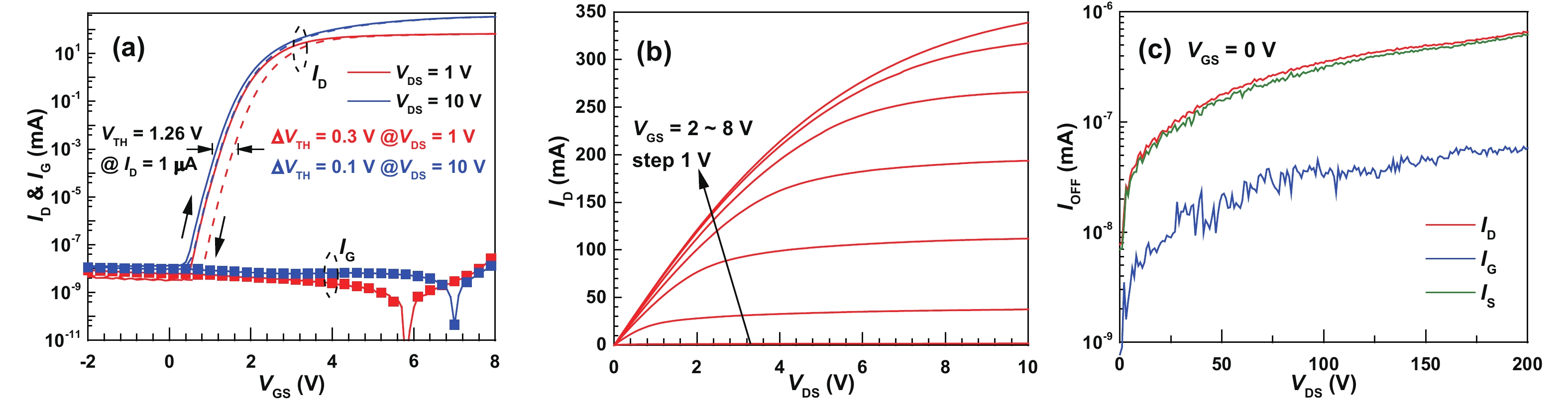
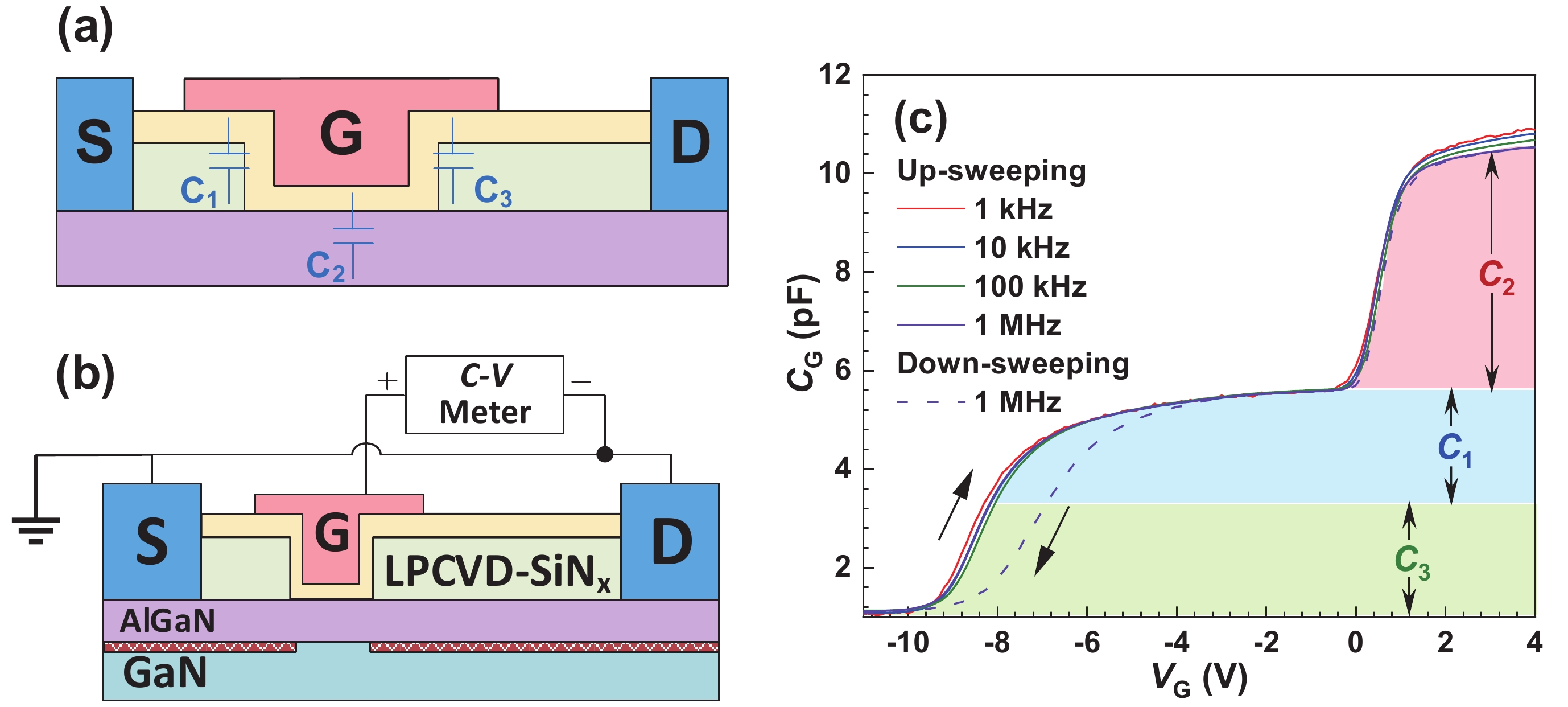
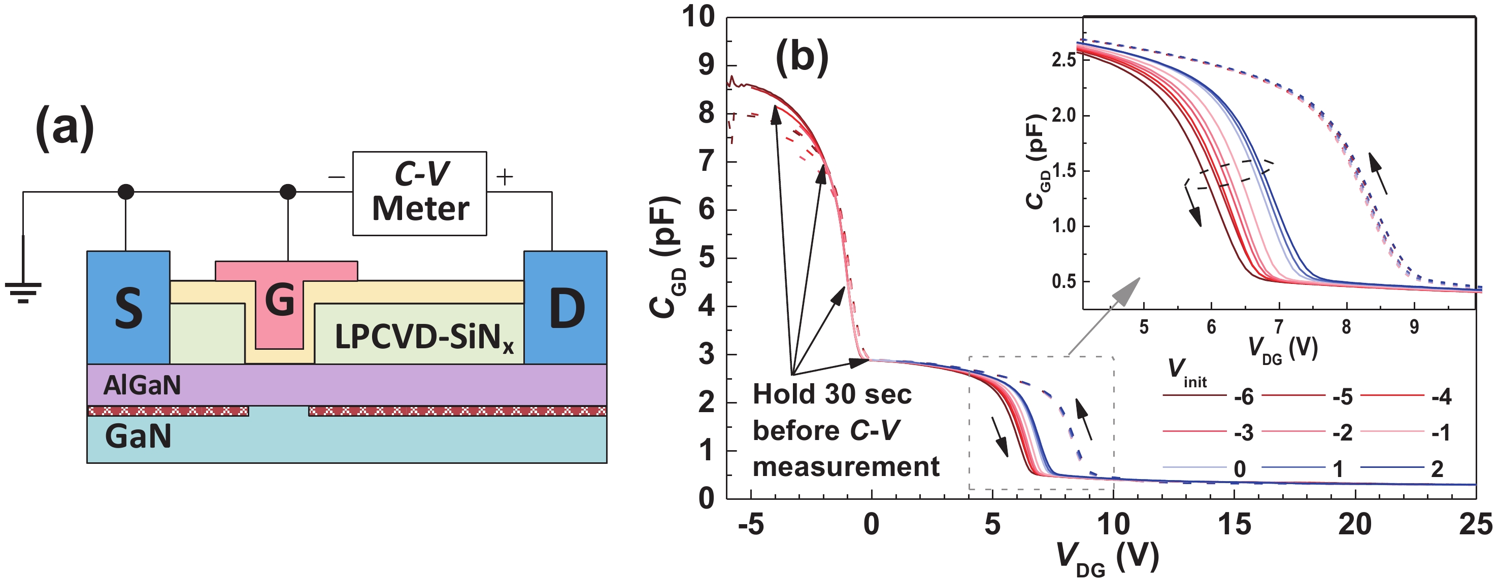
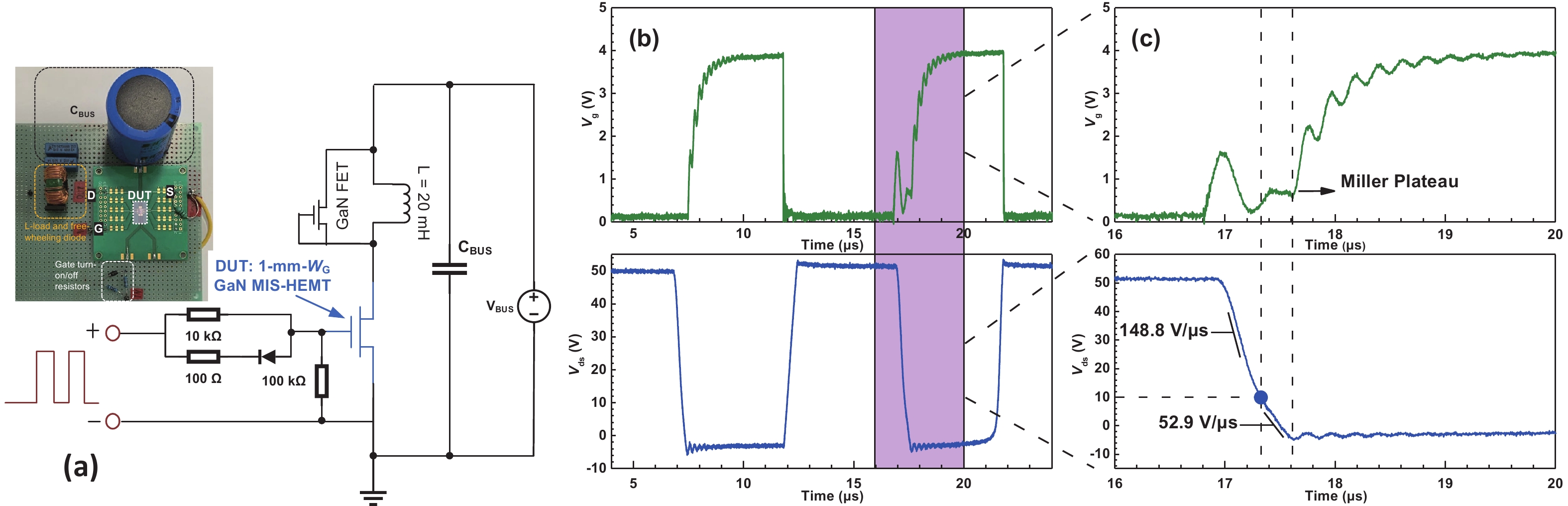
Fig. 1.
(Color online) (a) Cross sectional schematic of the E-mode AlGaN/GaN MIS-HEMT. (b) Microscope photograph of a 1-mm device.
ARTICLES
Lan Bi1, 2, Yixu Yao1, 2, Qimeng Jiang1, 2, , Sen Huang1, 2, , Xinhua Wang1, 2, Hao Jin1, 2, Xinyue Dai1, 2, Zhengyuan Xu1, Jie Fan1, 2, Haibo Yin1, 2, Ke Wei1, 2 and Xinyu Liu1, 2
Corresponding author: Qimeng Jiang, jiangqimeng@ime.ac.cn; Sen Huang, huangsen@ime.ac.cn
Abstract: Parasitic capacitances associated with overhangs of the T-shape-gate enhancement-mode (E-mode) GaN-based power device, were investigated by frequency/voltage-dependent capacitance–voltage and inductive-load switching measurements. The overhang capacitances induce a pinch-off voltage distinguished from that of the E-mode channel capacitance in the gate capacitance and the gate–drain capacitance characteristic curves. Frequency- and voltage-dependent tests confirm the instability caused by the trapping of interface/bulk states in the LPCVD-SiNx passivation dielectric. Circuit-level double pulse measurement also reveals its impact on switching transition for power switching applications.
Key words: AlGaN/GaN MIS-HEMTs, enhancement-mode, T-shape gate, parasitic capacitance, trapping/de-trapping, capacitance-voltage hysteresis
| [1] |
Boutros K S, Chu R M, Hughes B. GaN power electronics for automotive application. 2012 IEEE Energytech, 2012, 1
|
| [2] |
Piedra D, Lu B, Sun M, et al. Advanced power electronic devices based on gallium nitride (GaN). 2015 IEEE International Electron Devices Meeting, 2015, 16.6.1
|
| [3] |
Kizilyalli I C, Xu Y A, Carlson E, et al. Current and future directions in power electronic devices and circuits based on wide band-gap semiconductors. 2017 IEEE 5th Work Wide Bandgap Power Devices Appl, 2017, 417
|
| [4] |
Chen K J, H?berlen O, Lidow A, et al. GaN-on-Si power technology: Devices and applications. IEEE Trans Electron Devices, 2017, 64, 779 doi: 10.1109/TED.2017.2657579
|
| [5] |
Saito W, Nitta T, Kakiuchi Y, et al. Suppression of dynamic on-resistance increase and gate charge measurements in high-voltage GaN-HEMTs with optimized field-plate structure. IEEE Trans Electron Devices, 2007, 54, 1825 doi: 10.1109/TED.2007.901150
|
| [6] |
Chu R M, Corrion A, Chen M, et al. 1200-V normally off GaN-on-Si field-effect transistors with low dynamic on -resistance. IEEE Electron Device Lett, 2011, 32, 632 doi: 10.1109/LED.2011.2118190
|
| [7] |
Ma X B, Zhang J C, Guo L L, et al. Effects of passivation and FP structure on current collapse in an AlGaN/GaN HEMT. Chin J Semicond, 2007, 28, 73
|
| [8] |
Lei Y, Lu H. Influence of field plate on surface-state-related lag characteristics of AlGaN/GaN HEMT. J Semicond, 2015, 36, 074007 doi: 10.1088/1674-4926/36/7/074007
|
| [9] |
Meneghesso G, Bisi D, Rossetto I, et al. Reliability of power devices: Bias-induced threshold voltage instability and dielectric breakdown in GaN MIS-HEMTs. 2016 IEEE Int Integr Reliab Work, 2016, 35
|
| [10] |
Zhao R, Huang S, Wang X H, et al. Interface charge engineering in down-scaled AlGaN (<6 nm)/GaN heterostructure for fabrication of GaN-based power HEMTs and MIS-HEMTs. Appl Phys Lett, 2020, 116, 103502 doi: 10.1063/1.5134886
|
| [11] |
Yang S, Tang Z K, Hua M Y, et al. Investigation of SiN x and AlN passivation for AlGaN/GaN high-electron-mobility transistors: Role of interface traps and polarization charges. IEEE J Electron Devices Soc, 2020, 8, 358 doi: 10.1109/JEDS.2020.2984016
|
| [12] |
Viey A G, Vandendaele W, Jaud M A, et al. Investigation of nBTI degradation on GaN-on-Si E-mode MOSc-HEMT. 2019 IEEE International Electron Devices Meeting, 2019, 4.3.1
|
| [13] |
Huang S, Liu X, Wang X, et al. Ultrathin-barrier AlGaN/GaN heterostructure: a recess-free technology for manufacturing high-performance GaN-on-Si power devices. IEEE Trans on Electron Devices, 2018, 65, 207 doi: 10.1109/TED.2017.2773201
|
| [14] |
Huang S, Wang X H, Liu X Y, et al. Monolithic integration of E/D-mode GaN MIS-HEMTs on ultrathin-barrier AlGaN/GaN heterostructure on Si substrates. Appl Phys Express, 2019, 12, 024001 doi: 10.7567/1882-0786/aafa0e
|
| [15] |
Huang S, Liu X Y, Wang X H, et al. High uniformity normally-OFF GaN MIS-HEMTs fabricated on ultra-thin-barrier AlGaN/GaN heterostructure. IEEE Electron Device Lett, 2016, 37, 1617 doi: 10.1109/LED.2016.2617381
|
| [16] |
Guo F Q, Huang S, Wang X H, et al. Suppression of interface states between nitride-based gate dielectrics and ultrathin-barrier AlGaN/GaN heterostructure with in situ remote plasma pretreatments. Appl Phys Lett, 2021, 118, 093503 doi: 10.1063/5.0041421
|


Article views: 4498 Times PDF downloads: 416 Times Cited by: 0 Times
Received: 27 September 2021 Revised: 15 October 2021 Online: Uncorrected proof: 23 December 2021Accepted Manuscript: 23 December 2021Published: 10 March 2022
| Citation: |
Lan Bi, Yixu Yao, Qimeng Jiang, Sen Huang, Xinhua Wang, Hao Jin, Xinyue Dai, Zhengyuan Xu, Jie Fan, Haibo Yin, Ke Wei, Xinyu Liu. Instability of parasitic capacitance in T-shape-gate enhancement-mode AlGaN/GaN MIS-HEMTs[J]. Journal of Semiconductors, 2022, 43(3): 032801. doi: 10.1088/1674-4926/43/3/032801
****
L Bi, Y X Yao, Q M Jiang, S Huang, X H Wang, H Jin, X Y Dai, Z Y Xu, J Fan, H B Yin, K Wei, X Y Liu, Instability of parasitic capacitance in T-shape-gate enhancement-mode AlGaN/GaN MIS-HEMTs[J]. J. Semicond., 2022, 43(3): 032801. doi: 10.1088/1674-4926/43/3/032801.

|
| [1] |
Boutros K S, Chu R M, Hughes B. GaN power electronics for automotive application. 2012 IEEE Energytech, 2012, 1
|
| [2] |
Piedra D, Lu B, Sun M, et al. Advanced power electronic devices based on gallium nitride (GaN). 2015 IEEE International Electron Devices Meeting, 2015, 16.6.1
|
| [3] |
Kizilyalli I C, Xu Y A, Carlson E, et al. Current and future directions in power electronic devices and circuits based on wide band-gap semiconductors. 2017 IEEE 5th Work Wide Bandgap Power Devices Appl, 2017, 417
|
| [4] |
Chen K J, H?berlen O, Lidow A, et al. GaN-on-Si power technology: Devices and applications. IEEE Trans Electron Devices, 2017, 64, 779 doi: 10.1109/TED.2017.2657579
|
| [5] |
Saito W, Nitta T, Kakiuchi Y, et al. Suppression of dynamic on-resistance increase and gate charge measurements in high-voltage GaN-HEMTs with optimized field-plate structure. IEEE Trans Electron Devices, 2007, 54, 1825 doi: 10.1109/TED.2007.901150
|
| [6] |
Chu R M, Corrion A, Chen M, et al. 1200-V normally off GaN-on-Si field-effect transistors with low dynamic on -resistance. IEEE Electron Device Lett, 2011, 32, 632 doi: 10.1109/LED.2011.2118190
|
| [7] |
Ma X B, Zhang J C, Guo L L, et al. Effects of passivation and FP structure on current collapse in an AlGaN/GaN HEMT. Chin J Semicond, 2007, 28, 73
|
| [8] |
Lei Y, Lu H. Influence of field plate on surface-state-related lag characteristics of AlGaN/GaN HEMT. J Semicond, 2015, 36, 074007 doi: 10.1088/1674-4926/36/7/074007
|
| [9] |
Meneghesso G, Bisi D, Rossetto I, et al. Reliability of power devices: Bias-induced threshold voltage instability and dielectric breakdown in GaN MIS-HEMTs. 2016 IEEE Int Integr Reliab Work, 2016, 35
|
| [10] |
Zhao R, Huang S, Wang X H, et al. Interface charge engineering in down-scaled AlGaN (<6 nm)/GaN heterostructure for fabrication of GaN-based power HEMTs and MIS-HEMTs. Appl Phys Lett, 2020, 116, 103502 doi: 10.1063/1.5134886
|
| [11] |
Yang S, Tang Z K, Hua M Y, et al. Investigation of SiN x and AlN passivation for AlGaN/GaN high-electron-mobility transistors: Role of interface traps and polarization charges. IEEE J Electron Devices Soc, 2020, 8, 358 doi: 10.1109/JEDS.2020.2984016
|
| [12] |
Viey A G, Vandendaele W, Jaud M A, et al. Investigation of nBTI degradation on GaN-on-Si E-mode MOSc-HEMT. 2019 IEEE International Electron Devices Meeting, 2019, 4.3.1
|
| [13] |
Huang S, Liu X, Wang X, et al. Ultrathin-barrier AlGaN/GaN heterostructure: a recess-free technology for manufacturing high-performance GaN-on-Si power devices. IEEE Trans on Electron Devices, 2018, 65, 207 doi: 10.1109/TED.2017.2773201
|
| [14] |
Huang S, Wang X H, Liu X Y, et al. Monolithic integration of E/D-mode GaN MIS-HEMTs on ultrathin-barrier AlGaN/GaN heterostructure on Si substrates. Appl Phys Express, 2019, 12, 024001 doi: 10.7567/1882-0786/aafa0e
|
| [15] |
Huang S, Liu X Y, Wang X H, et al. High uniformity normally-OFF GaN MIS-HEMTs fabricated on ultra-thin-barrier AlGaN/GaN heterostructure. IEEE Electron Device Lett, 2016, 37, 1617 doi: 10.1109/LED.2016.2617381
|
| [16] |
Guo F Q, Huang S, Wang X H, et al. Suppression of interface states between nitride-based gate dielectrics and ultrathin-barrier AlGaN/GaN heterostructure with in situ remote plasma pretreatments. Appl Phys Lett, 2021, 118, 093503 doi: 10.1063/5.0041421
|

 WeChat ID
Journal of Semiconductors © 2017 All Rights Reserved 京ICP備05085259號-2
 DownLoad:

