


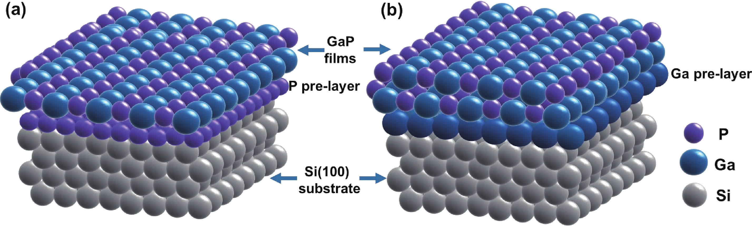
Fig. 1.
(Color online) Schematic illustration GaP/Si(100) heterostructure samples used in this work. (a) P-riched sample and (b) Ga-riched sample.
ARTICLES
Tieshi Wei1, 2, Xuefei Li1, , Zhiyun Li3, Wenxian Yang1, Yuanyuan Wu1, Zhiwei Xing1 and Shulong Lu1,
Corresponding author: Xuefei Li, xfli2011@sinano.ac.cn; Shulong Lu, sllu2008@sinano.ac.cn
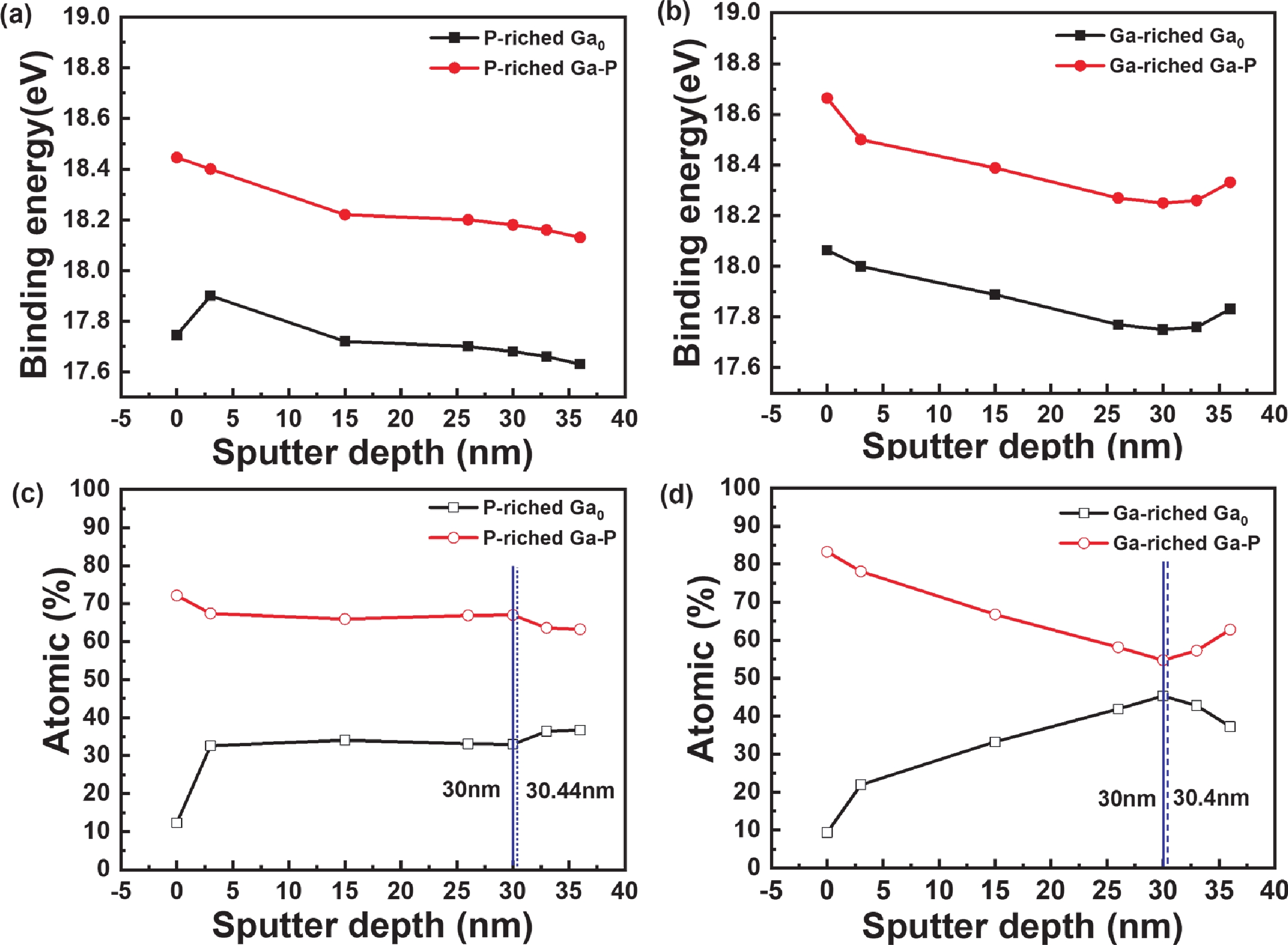
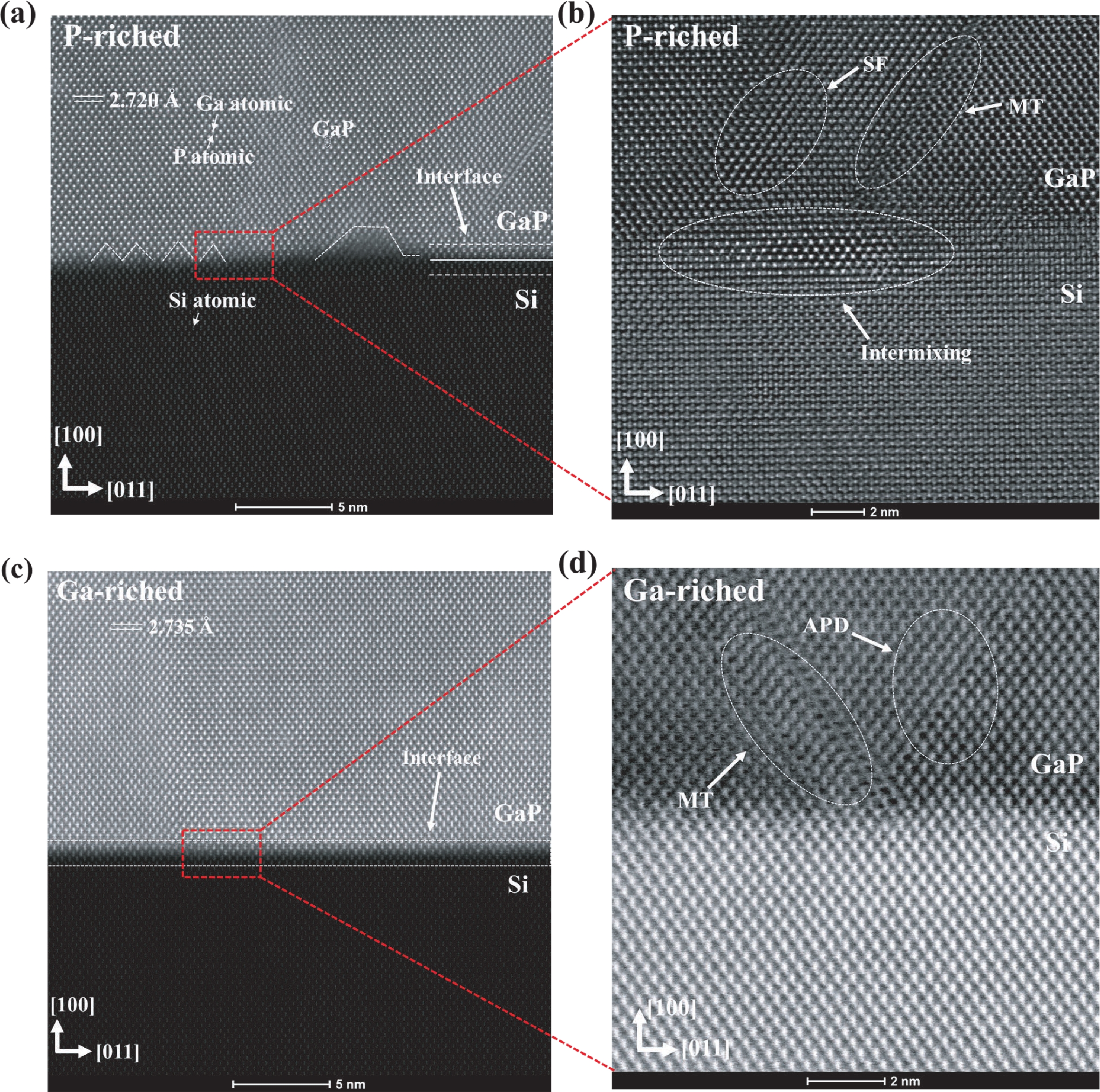
Abstract: The atomic structure and surface chemistry of GaP/Si(100) heterostructure with different pre-layers grown by molecular beam epitaxy are studied. It is found that GaP epilayer with Ga-riched pre-layers on Si(100) substrate has regular surface morphology and stoichiometric abrupt heterointerfaces from atomic force microscopes (AFMs) and spherical aberration-corrected transmission electron microscopes (ACTEMs). The interfacial dynamics of GaP/Si(100) heterostructure is investigated by X-ray photoelectron spectroscopy (XPS) equipped with an Ar gas cluster ion beam, indicating that Ga pre-layers can lower the interface formation energy and the bond that is formed is more stable. These results suggest that Ga-riched pre-layers are more conducive to the GaP nucleation as well as the epitaxial growth of GaP material on Si(100) substrate.
Key words: XPS, interfacial dynamics, GaP/Si(100) heterostructure, MBE
| [1] |
Boley A, Luna E, Zhang C, et al. Interfacial intermixing and anti-phase boundaries in GaP/Si(001) heterostructures. J Cryst Growth, 2021, 562, 126059 doi: 10.1016/j.jcrysgro.2021.126059
|
| [2] |
Boyer J T, Blumer A N, Blumer Z H, et al. Reduced dislocation lntroduction in III–V/Si heterostructures with glide-enhancing compressively strained superlattices. Cryst Growth Des, 2020, 20, 6939 doi: 10.1021/acs.cgd.0c00992
|
| [3] |
Zhang C, Vadiee E, Dahal S, et al. Developing high performance GaP/Si heterojunction solar cells. J Vis Exp, 2018, 141, 58292 doi: 10.3791/58292
|
| [4] |
Gutowski P, Sankowska I, S?upinski T, et al. Optimization of MBE growth conditions of In0.52Al0.48As waveguide layers for InGaAs/InAlAs/InP quantum cascade lasers. Materials, 2019, 12, 1621 doi: 10.3390/ma12101621
|
| [5] |
Han Y, Ng W K, Xue Y, et al. Room temperature III–V nanolasers with distributed bragg reflectors epitaxially grown on (001) silicon-on-insulators. Photonics Res, 2019, 7, 1081 doi: 10.1364/PRJ.7.001081
|
| [6] |
Kawanami H. Heteroepitaxial technologies of III–V on Si. Sol Energy Mater Sol Cells, 2001, 66, 479 doi: 10.1016/S0927-0248(00)00209-9
|
| [7] |
Fang S F, Adomi K, Lyer S, et al. Gallium arsenide and other compound semiconductors on silicon. J Appl Phys, 1990, 68, R31 doi: 10.1063/1.346284
|
| [8] |
Supplie O, Romanyuk O, Koppka C, et al. Metalorganic vapor phase epitaxy of III–V-on-silicon: experiment and theory. Prog Cryst Growth Charact Mater, 2018, 64, 103 doi: 10.1016/j.pcrysgrow.2018.07.002
|
| [9] |
Feifel M, Ohlmann J, France R M, et al. Electron channeling contrast imaging investigation of stacking fault pyramids in GaP on Si nucleation layers. J Cryst Growth, 2020, 532, 125422 doi: 10.1016/j.jcrysgro.2019.125422
|
| [10] |
Harrison W A, Kraut E A, Waldrop J R, et al. Polar heterojunction interfaces. Phys Rev B, 1978, 18, 4402 doi: 10.1103/PhysRevB.18.4402
|
| [11] |
Zhang C, Boley A, Faleev N, et al. Investigation of defect creation in GaP/Si(001) epitaxial structures. J Cryst Growth, 2018, 503, 36 doi: 10.1016/j.jcrysgro.2018.09.020
|
| [12] |
Grassman T J, Brenner M R, Rajagopalan S, et al. Control and elimination of nucleation-related defects in GaP/Si(001) heteroepitaxy. Appl Phys Lett, 2009, 94, 232106 doi: 10.1063/1.3154548
|
| [13] |
Lucci I, Charbonnier S, Vallet M, et al. A stress-free and textured GaP template on silicon for solar water splitting. Adv Funct Mater, 2018, 28, 1801585 doi: 10.1002/adfm.201801585
|
| [14] |
Hool R D, Chai Y, Sun Y, et al. Relaxed GaP on Si with low threading dislocation density. Appl Phys Lett, 2020, 116, 042102 doi: 10.1063/1.5141122
|
| [15] |
Romanyuk O, Gordeev I, Paszuk A, et al. GaP/Si(001) interface study by XPS in combination with Ar gas cluster ion beam sputtering. Appl Surf Sci, 2020, 514, 145903 doi: 10.1016/j.apsusc.2020.145903
|
| [16] |
Doscher H, Bruckner S, Dobrich A, et al. Surface preparation of Si(100) by thermal oxide removal in a chemical vapor environment. J Cryst Growth, 2011, 315, 10 doi: 10.1016/j.jcrysgro.2010.07.017
|
| [17] |
Nandy M, Paszuk A, Feifel M, et al. A route to obtaining low-defect III–V epilayers on Si (100) utilizing MOCVD. Cryst Growth Des, 2021, 21, 5603 doi: 10.1021/acs.cgd.1c00410
|
| [18] |
D. Keith Bowen and Tanner. B K, High resolution X-ray diffractometry and topography. Abingdon, Taylor & Francis e-Library, 1998
|
| [19] |
Chadi D J. Stabilities of single-layer and bilayer steps on Si (001) surfaces. Phys Rev Lett, 1987, 59, 1691 doi: 10.1103/PhysRevLett.59.1691
|
| [20] |
Curson N J, Schofield S R, Simmons M Y, et al. STM characterization of the Si-P heterodimer. Phys Rev B, 2004, 69, 195303 doi: 10.1103/PhysRevB.69.195303
|
| [21] |
Brenner M R. GaP/Si heteroepitaxy (suppression of nucleation related defects). Ohio, The Ohio State University, 2009
|
| [22] |
Suzuki Y, Sanada N, Shimomura M, et al. High-resolution XPS analysis of GaP(001), (111)A, and (111)B surfaces passivated by (NH4)2S x solution. Appl Surf Sci, 2004, 235, 260 doi: 10.1016/j.apsusc.2004.05.099
|
| [23] |
Supplie O, May M M, Steinbach G, et al. Time-resolved in Situ spectroscopy during formation of the GaP/Si(100) heterointerface. J Phys Chem Lett, 2015, 6, 464 doi: 10.1021/jz502526e
|
| [24] |
Liu K Z, Suzuki Y, Fukuda Y. AES and XPS studies of a GaP(001) surface treated by S2Cl2 and P2S5/(NH4)2S x. Appl Surf Sci, 2004, 237, 627 doi: 10.1016/j.apsusc.2004.06.135
|
| [25] |
Beyer A, Stegmu?ller A, Oelerich J O, et al. Pyramidal structure formation at the lnterface between III/V semiconductors and silicon. Chem Mater, 2016, 28, 3265 doi: 10.1021/acs.chemmater.5b04896
|
| [26] |
Nagano M, Yamada S, Akita S, et al. Low-damage sputtering of GaAs and GaP using size-selected Ar cluster ion beams. Jpn J Appl Phys, 2005, 44, 164 doi: 10.1143/JJAP.44.L164
|
| [27] |
Romanyuk O, Hannappel T, Grosse F. Atomic and electronic structure of GaP/Si(111), GaP/Si(110), and GaP/Si(113) interfaces and superlattices studied by density functional theory. Phys Rev B, 2013, 88, 115312 doi: 10.1103/PhysRevB.88.115312
|
| [28] |
Baira M, Bekhti-Siad A, Hebali K, et al. Charge compensation mechanisms in favor of the incorporation of the Eu3+ ion into the ZnO host lattice. Phys B, 2018, 537, 296 doi: 10.1016/j.physb.2018.02.035
|
| [29] |
Romanyuk O, Grosse F, Braun W. Stoichiometry and bravais lattice diversity: Anab initiostudy of the GaSb(001) surface. Phys Rev B, 2009, 79, 235330 doi: 10.1103/PhysRevB.79.235330
|
| [30] |
Doscher H, Supplie O, Bruckner S, et al. Indirect in situ characterization of Si(100) substrates at the initial stage of III–V heteroepitaxy. J Cryst Growth, 2011, 315, 16 doi: 10.1016/j.jcrysgro.2010.08.017
|
| [31] |
P Farin, H Eisele, D?hne M. From surface data to bulk properties: a case study for antiphase boundaries in GaP on Si (001). J Phys D, 2021, 54, 205302 doi: 10.1088/1361-6463/abdff1
|
| [32] |
Volz K, Beyer A, Witte W, et al. GaP-nucleation on exact Si (001) substrates for III/V device integration. J Cryst Growth, 2011, 315, 37 doi: 10.1016/j.jcrysgro.2010.10.036
|


Article views: 2214 Times PDF downloads: 87 Times Cited by: 0 Times
Received: 12 June 2022 Revised: 19 July 2022 Online: Accepted Manuscript: 08 September 2022Uncorrected proof: 08 September 2022Published: 02 December 2022
| Citation: |
Tieshi Wei, Xuefei Li, Zhiyun Li, Wenxian Yang, Yuanyuan Wu, Zhiwei Xing, Shulong Lu. Interfacial dynamics of GaP/Si(100) heterostructure grown by molecular beam epitaxy[J]. Journal of Semiconductors, 2022, 43(12): 122101. doi: 10.1088/1674-4926/43/12/122101
****
T S Wei, X F Li, Z Y Li, W X Yang, Y Y Wu, Z W Xing, S L Lu. Interfacial dynamics of GaP/Si(100) heterostructure grown by molecular beam epitaxy[J]. J. Semicond, 2022, 43(12): 122101. doi: 10.1088/1674-4926/43/12/122101

|
| [1] |
Boley A, Luna E, Zhang C, et al. Interfacial intermixing and anti-phase boundaries in GaP/Si(001) heterostructures. J Cryst Growth, 2021, 562, 126059 doi: 10.1016/j.jcrysgro.2021.126059
|
| [2] |
Boyer J T, Blumer A N, Blumer Z H, et al. Reduced dislocation lntroduction in III–V/Si heterostructures with glide-enhancing compressively strained superlattices. Cryst Growth Des, 2020, 20, 6939 doi: 10.1021/acs.cgd.0c00992
|
| [3] |
Zhang C, Vadiee E, Dahal S, et al. Developing high performance GaP/Si heterojunction solar cells. J Vis Exp, 2018, 141, 58292 doi: 10.3791/58292
|
| [4] |
Gutowski P, Sankowska I, S?upinski T, et al. Optimization of MBE growth conditions of In0.52Al0.48As waveguide layers for InGaAs/InAlAs/InP quantum cascade lasers. Materials, 2019, 12, 1621 doi: 10.3390/ma12101621
|
| [5] |
Han Y, Ng W K, Xue Y, et al. Room temperature III–V nanolasers with distributed bragg reflectors epitaxially grown on (001) silicon-on-insulators. Photonics Res, 2019, 7, 1081 doi: 10.1364/PRJ.7.001081
|
| [6] |
Kawanami H. Heteroepitaxial technologies of III–V on Si. Sol Energy Mater Sol Cells, 2001, 66, 479 doi: 10.1016/S0927-0248(00)00209-9
|
| [7] |
Fang S F, Adomi K, Lyer S, et al. Gallium arsenide and other compound semiconductors on silicon. J Appl Phys, 1990, 68, R31 doi: 10.1063/1.346284
|
| [8] |
Supplie O, Romanyuk O, Koppka C, et al. Metalorganic vapor phase epitaxy of III–V-on-silicon: experiment and theory. Prog Cryst Growth Charact Mater, 2018, 64, 103 doi: 10.1016/j.pcrysgrow.2018.07.002
|
| [9] |
Feifel M, Ohlmann J, France R M, et al. Electron channeling contrast imaging investigation of stacking fault pyramids in GaP on Si nucleation layers. J Cryst Growth, 2020, 532, 125422 doi: 10.1016/j.jcrysgro.2019.125422
|
| [10] |
Harrison W A, Kraut E A, Waldrop J R, et al. Polar heterojunction interfaces. Phys Rev B, 1978, 18, 4402 doi: 10.1103/PhysRevB.18.4402
|
| [11] |
Zhang C, Boley A, Faleev N, et al. Investigation of defect creation in GaP/Si(001) epitaxial structures. J Cryst Growth, 2018, 503, 36 doi: 10.1016/j.jcrysgro.2018.09.020
|
| [12] |
Grassman T J, Brenner M R, Rajagopalan S, et al. Control and elimination of nucleation-related defects in GaP/Si(001) heteroepitaxy. Appl Phys Lett, 2009, 94, 232106 doi: 10.1063/1.3154548
|
| [13] |
Lucci I, Charbonnier S, Vallet M, et al. A stress-free and textured GaP template on silicon for solar water splitting. Adv Funct Mater, 2018, 28, 1801585 doi: 10.1002/adfm.201801585
|
| [14] |
Hool R D, Chai Y, Sun Y, et al. Relaxed GaP on Si with low threading dislocation density. Appl Phys Lett, 2020, 116, 042102 doi: 10.1063/1.5141122
|
| [15] |
Romanyuk O, Gordeev I, Paszuk A, et al. GaP/Si(001) interface study by XPS in combination with Ar gas cluster ion beam sputtering. Appl Surf Sci, 2020, 514, 145903 doi: 10.1016/j.apsusc.2020.145903
|
| [16] |
Doscher H, Bruckner S, Dobrich A, et al. Surface preparation of Si(100) by thermal oxide removal in a chemical vapor environment. J Cryst Growth, 2011, 315, 10 doi: 10.1016/j.jcrysgro.2010.07.017
|
| [17] |
Nandy M, Paszuk A, Feifel M, et al. A route to obtaining low-defect III–V epilayers on Si (100) utilizing MOCVD. Cryst Growth Des, 2021, 21, 5603 doi: 10.1021/acs.cgd.1c00410
|
| [18] |
D. Keith Bowen and Tanner. B K, High resolution X-ray diffractometry and topography. Abingdon, Taylor & Francis e-Library, 1998
|
| [19] |
Chadi D J. Stabilities of single-layer and bilayer steps on Si (001) surfaces. Phys Rev Lett, 1987, 59, 1691 doi: 10.1103/PhysRevLett.59.1691
|
| [20] |
Curson N J, Schofield S R, Simmons M Y, et al. STM characterization of the Si-P heterodimer. Phys Rev B, 2004, 69, 195303 doi: 10.1103/PhysRevB.69.195303
|
| [21] |
Brenner M R. GaP/Si heteroepitaxy (suppression of nucleation related defects). Ohio, The Ohio State University, 2009
|
| [22] |
Suzuki Y, Sanada N, Shimomura M, et al. High-resolution XPS analysis of GaP(001), (111)A, and (111)B surfaces passivated by (NH4)2S x solution. Appl Surf Sci, 2004, 235, 260 doi: 10.1016/j.apsusc.2004.05.099
|
| [23] |
Supplie O, May M M, Steinbach G, et al. Time-resolved in Situ spectroscopy during formation of the GaP/Si(100) heterointerface. J Phys Chem Lett, 2015, 6, 464 doi: 10.1021/jz502526e
|
| [24] |
Liu K Z, Suzuki Y, Fukuda Y. AES and XPS studies of a GaP(001) surface treated by S2Cl2 and P2S5/(NH4)2S x. Appl Surf Sci, 2004, 237, 627 doi: 10.1016/j.apsusc.2004.06.135
|
| [25] |
Beyer A, Stegmu?ller A, Oelerich J O, et al. Pyramidal structure formation at the lnterface between III/V semiconductors and silicon. Chem Mater, 2016, 28, 3265 doi: 10.1021/acs.chemmater.5b04896
|
| [26] |
Nagano M, Yamada S, Akita S, et al. Low-damage sputtering of GaAs and GaP using size-selected Ar cluster ion beams. Jpn J Appl Phys, 2005, 44, 164 doi: 10.1143/JJAP.44.L164
|
| [27] |
Romanyuk O, Hannappel T, Grosse F. Atomic and electronic structure of GaP/Si(111), GaP/Si(110), and GaP/Si(113) interfaces and superlattices studied by density functional theory. Phys Rev B, 2013, 88, 115312 doi: 10.1103/PhysRevB.88.115312
|
| [28] |
Baira M, Bekhti-Siad A, Hebali K, et al. Charge compensation mechanisms in favor of the incorporation of the Eu3+ ion into the ZnO host lattice. Phys B, 2018, 537, 296 doi: 10.1016/j.physb.2018.02.035
|
| [29] |
Romanyuk O, Grosse F, Braun W. Stoichiometry and bravais lattice diversity: Anab initiostudy of the GaSb(001) surface. Phys Rev B, 2009, 79, 235330 doi: 10.1103/PhysRevB.79.235330
|
| [30] |
Doscher H, Supplie O, Bruckner S, et al. Indirect in situ characterization of Si(100) substrates at the initial stage of III–V heteroepitaxy. J Cryst Growth, 2011, 315, 16 doi: 10.1016/j.jcrysgro.2010.08.017
|
| [31] |
P Farin, H Eisele, D?hne M. From surface data to bulk properties: a case study for antiphase boundaries in GaP on Si (001). J Phys D, 2021, 54, 205302 doi: 10.1088/1361-6463/abdff1
|
| [32] |
Volz K, Beyer A, Witte W, et al. GaP-nucleation on exact Si (001) substrates for III/V device integration. J Cryst Growth, 2011, 315, 37 doi: 10.1016/j.jcrysgro.2010.10.036
|

 WeChat ID
Journal of Semiconductors © 2017 All Rights Reserved 京ICP備05085259號-2
 DownLoad:

